


Member News
【Member News】Garen Semiconductor Xia Ning:Large-Size Gallium Oxide Single-Crystal Growth and Defects
日期:2025-12-15阅读:604
As a fourth-generation semiconductor material, Gallium Oxide features an ultra-wide bandgap (4.8 eV) and an exceptionally high critical breakdown field (8 MV/cm), offering significant advantages in high-voltage tolerance, high-temperature operation, high-frequency performance, and radiation resistance. Its unique ultraviolet transparency (with a transmittance exceeding 80%) and relatively low fabrication cost further broaden its application prospects. In the short term, Gallium Oxide is expected to enable breakthroughs in extreme-condition defense materials; in the long term, it is poised to empower a civilian market worth hundreds of billions.
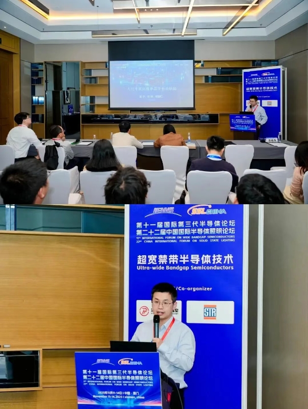
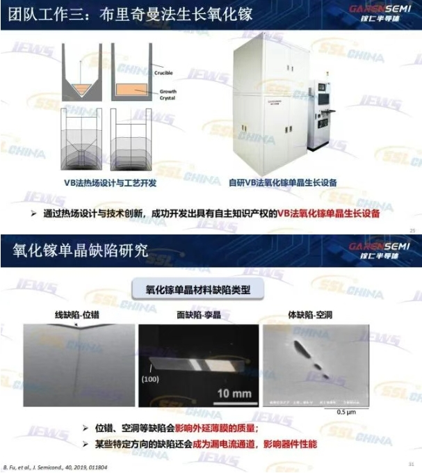
Recently, at the 11th International Forum on Wide Bandgap Semiconductors & the 22nd China International Forum on Solid State Lighting (IFWS & SSLCHINA 2025), Xia Ning, Chief Technology Officer of Hangzhou Garen Semiconductor Co., Ltd., was invited to attend and delivered a keynote presentation entitled “Large-Size Gallium Oxide Single-Crystal Growth and Defects” in the “Ultra-Wide Bandgap Semiconductor Technologies” session. The report covered Gallium Oxide single-crystal growth technologies, including Czochralski pulling, casting, and Vertical Bridgman (VB) methods, as well as defect studies in Gallium Oxide.
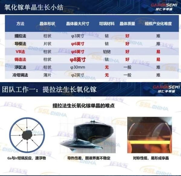
Gallium Oxide crystal growth faces multiple challenges: volatility and decomposition at high temperatures requiring oxygen-containing growth environments; the combination of high melting point and oxidizing conditions, which severely limits crucible material choices and necessitates the redevelopment of growth equipment and techniques; as well as poor thermal conductivity and strong free-carrier absorption, leading to extreme instability at the solid–liquid interface.
Xia Ning noted that there are many Gallium Oxide crystal growth methods. At present, the floating-zone and cold-crucible methods show little industrial potential; the Czochralski method faces scalability challenges; and the EFG method, while currently applied, lacks competitiveness for large-scale industrialization due to cost constraints. In contrast, casting and VB methods demonstrate strong potential for large-scale industrialization in terms of size, cost, and quality. The presentation systematically reviewed recent research progress in Gallium Oxide growth via the Czochralski, casting, and Bridgman methods.
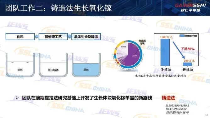
According to Xia Ning, the developed casting-based technologies have successfully enabled the growth of large-size (8-inch) Gallium Oxide crystals with multiple crystal orientations and various doping types, meeting diverse epitaxial and device requirements. Cost estimates indicate that once mass production is achieved, the cost of 8-inch substrates can be reduced to below RMB 2,000, with further cost reductions expected within the next two to three years, providing the industry with high-quality, low-cost substrates. Such substrates will help address key challenges including large-area epitaxy, defect behavior, p-type doping, and large-area high-current devices. The industrialization of Gallium Oxide is expected to accelerate, with closer integration across substrates, epitaxy, devices, and applications to achieve breakthroughs.
Company Profile
Founded in September 2022, Hangzhou Garen Semiconductor Co., Ltd. is a technology-driven enterprise specializing in the R&D, production, and sales of wide-bandgap semiconductor materials such as Gallium Oxide. Leveraging the State Key Laboratory of Silicon and Advanced Semiconductor Materials at Zhejiang University and the Zhejiang University Hangzhou International Science and Innovation Center, the company has built a strong R&D, production, and operations team led by an academician of the Chinese Academy of Sciences as chief advisor.
Garen Semiconductor has pioneered new Gallium Oxide single-crystal growth technologies and has secured 14 international and domestic invention patents, breaking Western monopolies and technological blockades in Gallium Oxide substrate materials. Oriented toward addressing major national needs, the company is committed to sustained innovation in the upstream Gallium Oxide industry chain, striving to provide reliable material support for China’s power electronics and related industries.
By leading industry innovation, Garen Semiconductor has adopted proprietary casting and other novel single-crystal growth technologies to achieve breakthroughs in the production of 8-inch Gallium Oxide single-crystal substrates and wafer-scale (010)-oriented single-crystal substrates. The company has also developed the first Gallium Oxide–dedicated VB crystal growth system with an integrated process package. Garen Semiconductor has mastered core technologies across the entire Gallium Oxide value chain—including crystal growth, processing, and epitaxy—and provides customers with large-size, high-quality Gallium Oxide products and equipment backed by fully independent intellectual property rights.
