


Member News
【Member News】Suzhou Raphael Optech Showcases at APCSCRM 2025: Spotlight on Semiconductor Technologies and Products
日期:2025-12-15阅读:611
At the 6th Asia Pacific Conference on Silicon Carbide and Related Materials (APCSCRM 2025), Gallium Oxide emerged as one of the most prominent focal points in the field. As an invited participant, the Asian Gallium Oxide Alliance (AGOA) conducted an interview with its council member—Suzhou Raphael Optech Co.,Ltd.—during the conference. In the following section, we take a closer look at Raphael Optech, its core businesses, and its flagship products as presented.
Suzhou Raphael Optech Co., Ltd.
Suzhou Raphael Optech Co., Ltd. is a national high-tech enterprise specializing in optical 3D inspection, and has been recognized as a Gusu Leading Talent Enterprise and a Jiangsu Province “Double Innovation” Talent Enterprise. The company is a member of the National Technical Committee for Optics and Photonics Standardization and its Microscopy Subcommittee.
The company has developed mature optical inspection solutions for semiconductor manufacturing, and has independently developed product lines including wafer warpage and thin-film stress measurement systems, wafer in-plane stress inspection systems, and wafer geometric and topography measurement instruments. These solutions have achieved partial substitution of imported equipment, providing users with cost-effective inspection products and services.
Suzhou Raphael Optech is committed to addressing key inspection bottlenecks that limit semiconductor material applications, such as micro-/nano-scale surface morphology characterization, stress distribution analysis, and defect identification. Guided by the mission of “meticulous attention to detail and continuous pursuit of excellence,” the company focuses on the semiconductor wafer inspection field and, through independent innovation, has developed a series of industry-leading inspection technologies and equipment. Its product portfolio covers both laboratory use (semi-automatic systems) and high-volume manufacturing lines (fully automatic systems), meeting the needs of diverse application scenarios. By enabling precise inspection, the company helps improve yield, significantly reduce downstream manufacturing costs, enhance inspection efficiency, and shorten product development cycles. Looking ahead, Suzhou Raphael Optech will continue to invest in innovation in semiconductor inspection technologies, striving to become a global leader in high-end semiconductor inspection equipment and to contribute to worldwide semiconductor technology advancement.
Product Portfolio
Product 1: Fully Automatic Wafer Geometric Topography Measurement System
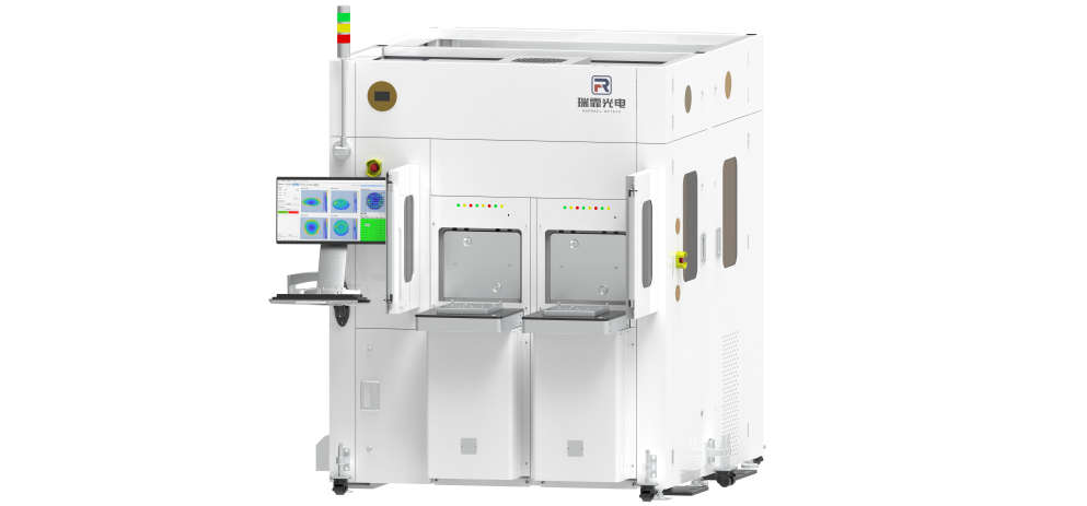
Designed for high-precision measurement of wafer geometric parameters during semiconductor manufacturing, this system measures wafer thickness (THK), total thickness variation (TTV), local thickness variation (LTV), bow, warp, and total indicator reading (TIR). By integrating an EFEM module, it enables fully automated measurement of wafer geometric parameters.
Product 2: Fully Automatic Wafer Warpage and Thin-Film Stress Measurement System
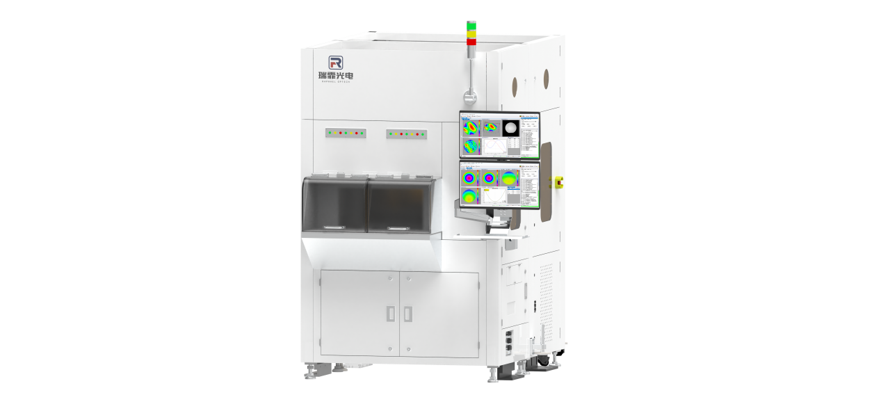
Used for one-time, full-aperture, high-precision measurement of wafer three-dimensional warpage (bow and warp) and thin-film stress during semiconductor manufacturing. Based on structured-light phase deflectometry, the system supports stress measurement on transparent, semi-transparent, or opaque polished wafers, as well as patterned wafers, and is widely applied in thin-film process R&D and production monitoring.
Product 3: Automatic Wafer Microscopic Profilometer
The WMT-300 wafer microscopic 3D topography measurement system measures micro-scale features such as steps, deep trenches, and trench widths, as well as macro-scale features such as photoresist thickness distribution. Through dedicated software, it enables semi-automatic 3D surface topography measurement, automatic data processing and analysis, and extraction of 2D and 3D parameters, providing comprehensive three-dimensional characterization of device wafers.
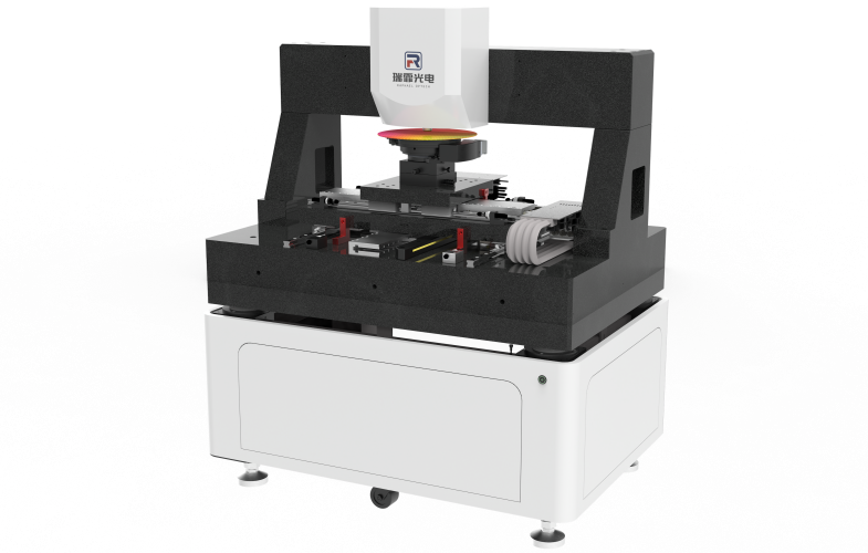
Product 4: SV200-i Fully Automatic Internal Stress Measurement System

Designed for fully automated internal stress measurement of wafers such as SiC, GaN, Si, and quartz, the SV200-i offers high-precision quantitative analysis and production-level statistical functions. It is well suited for compound-semiconductor wafer seed crystal screening, crystal growth quality control, wafer processing process monitoring, and finished wafer quality assurance throughout the entire wafer manufacturing process.
Product 5: Multi-Mode 3D Microscope

The multi-mode 3D microscope integrates three measurement modes—nanometer-scale white-light interferometry, spectral confocal scanning, and extended-depth-of-field image fusion—into a single system, offering exceptional adaptability across a wide range of application scenarios.
