Paper Sharing
【Member Papers】2.3-kV β-Ga₂O₃ heterojunction barrier Schottky diode with Cu anode and robust thermal reliability
日期:2025-12-16阅读:590
Researchers from the Southern University of Science and Technology and Shenzhen Polytechnic University have published a dissertation titled "2.3-kV β-Ga2O3 heterojunction barrier Schottky diode with Cu anode and robust thermal reliability" in Applied Physics Letters.
Project Support
This work was supported by National Natural Science Foundation of China (Grant No: 62274082). Research on mechanism of source/drain ohmic contact and the related GaN p-FET (Grant No: 2023A1515030034). Study on the reliability of GaN power devices (Grant No: JCYJ20220818100605012). Research on novelty low-resistance Source/Drain ohmic contact for GaN p-FET (Grant No: JCYJ20220530115411025). Research on GaN-Based Devices for Industrial Applications (Grant No. 6025312001K). The authors also acknowledge the assistance of SUSTech Core Research Facilities.
Background
Beta-Gallium oxide (β-Ga2O3), with its 4.8 eV ultra-wide bandgap, high critical breakdown field of up to 8 MV/cm, and availability of large-area substrates, is considered a leading candidate for high-voltage power electronics. However, β-Ga2O3 diodes still face a trade-off between conduction loss and breakdown voltage. To mitigate this issue, the heterojunction barrier Schottky (JBS) structure has been proposed to combine the low turn-on voltage of Schottky diodes with the enhanced blocking capability of heterojunction diodes. In addition, low–work function metal anodes such as Mo and TiN have been utilized to further reduce the Schottky barrier height, effectively lowering the turn-on voltage while maintaining reasonably high breakdown performance, underscoring the importance of anode engineering. Nonetheless, barrier height reduction often degrades breakdown capability, and the long-term reliability and degradation pathways of such devices remain insufficiently characterized, limiting their broader adoption in high-voltage applications.
Abstract
β-Ga2O3 power diodes inherently face challenges in balancing forward conduction loss and reverse blocking capability. To address this limitation, we developed a high-performance Cu2O/β-Ga2O3 heterojunction barrier Schottky (JBS) diode deploying a low work function copper (Cu) anode. The device simultaneously achieves a low turn-on voltage of 0.83 V, a breakdown voltage of 2345 V, and a power figure-of-merit of 1.22 GW/cm2. Additionally, temperature-dependent measurements confirm that the Pt/Cu2O structure enhances the barrier height and suppresses the reverse saturation current, further improving breakdown performance. Under a 200 V reverse stress at 425 K for 104 s, the JBS diode exhibits only a 1.316-fold increase in dynamic on-resistance and a 10.76% degradation in turn-on voltage, highlighting excellent long-term thermal and electrical reliability. These findings suggest a promising strategy for β-Ga2O3-based power electronics with superior performance and reliability.
Conclusion
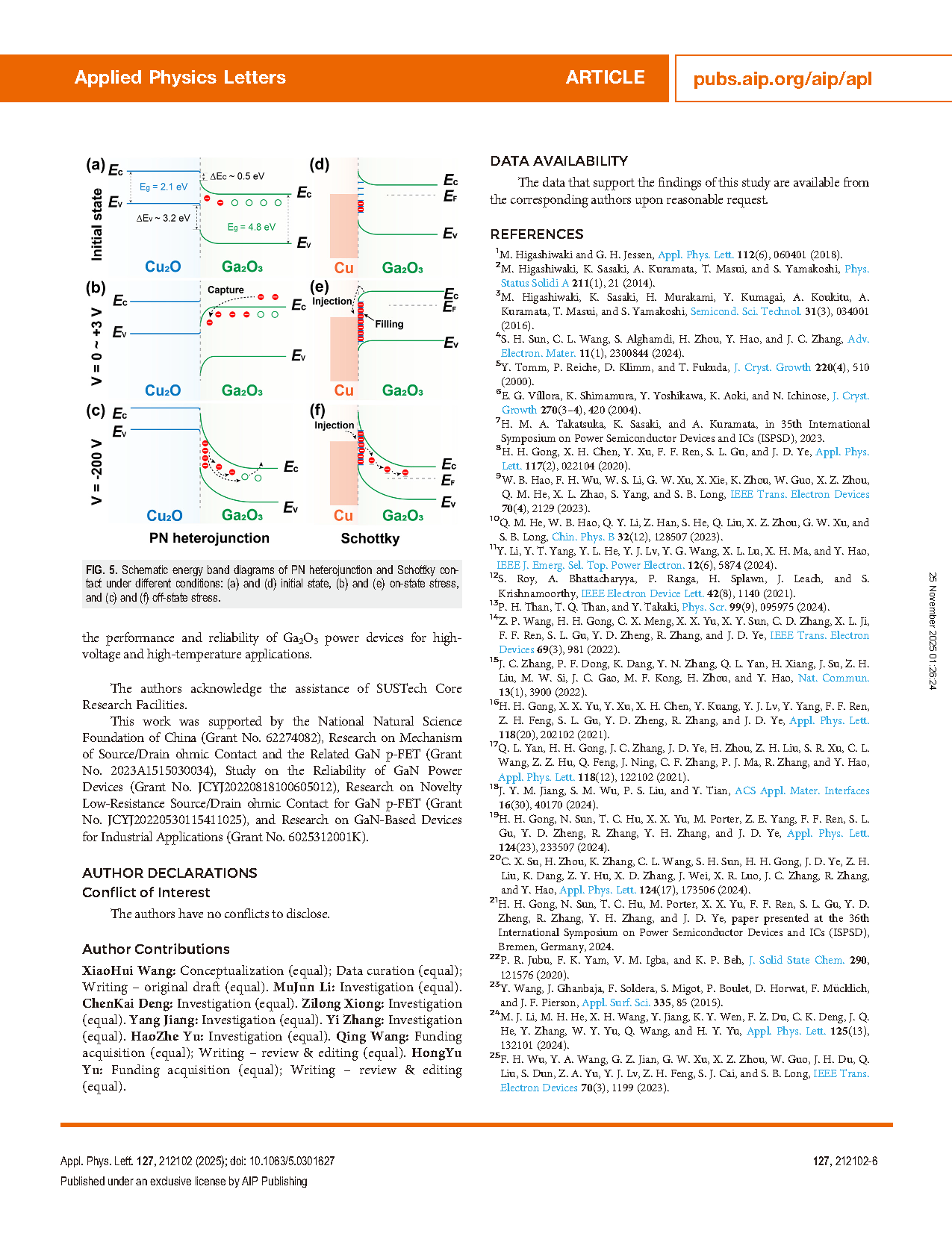
In summary, we proposed a Cu2O/Ga2O3 JBS diode with a low work function Cu anode, simultaneously achieving a low VON of 0.83 V and a high BV of 2345 V. The JBS diode also demonstrates a low Ron,sp of 4.52 mΩ·cm2 and a high PFOM of 1.22 GW/cm2. This performance stems from the Cu anode reducing ΦB and the Cu2O/Ga2O3 heterojunction enhancing depletion in reverse bias. The JBS diode exhibits a 1.316-fold increase in Ron,sp,dyn/Ron,sp ratio and a 10.76% degradation in VON under a 200 V reverse stress at 425 K for 104 s. With the increasing stress time, the ionization of interface traps broadens the current conduction path, leading to increased Ron,sp and VON. These results demonstrate a promising strategy for advancing the performance and reliability of Ga2O3 power devices for high-voltage and high-temperature applications
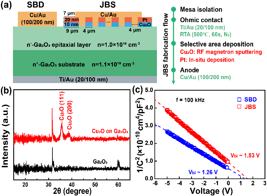
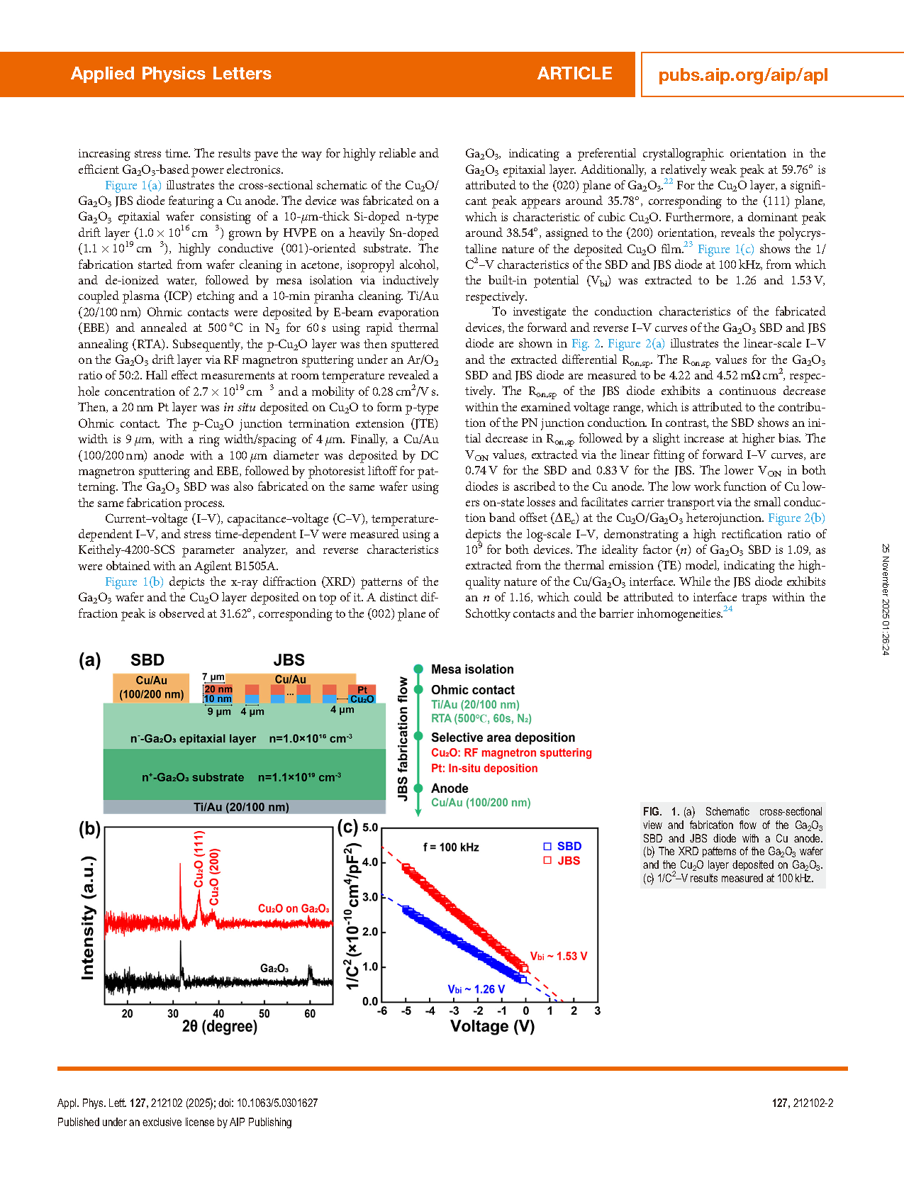
Fig. 1. (a) Schematic cross-sectional view and fabrication flow of the Ga2O3 SBD and JBS diodes with a Cu anode. (b) The XRD patterns of the Ga2O3 wafer and the Cu2O layer deposited on Ga2O3. (c) 1/C2-V results measured at 100 kHz.
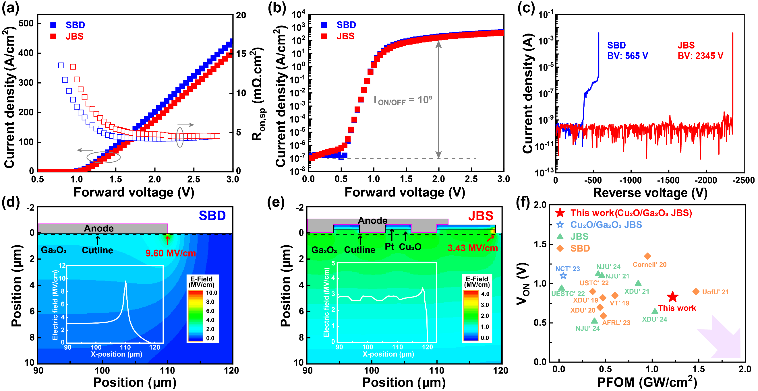
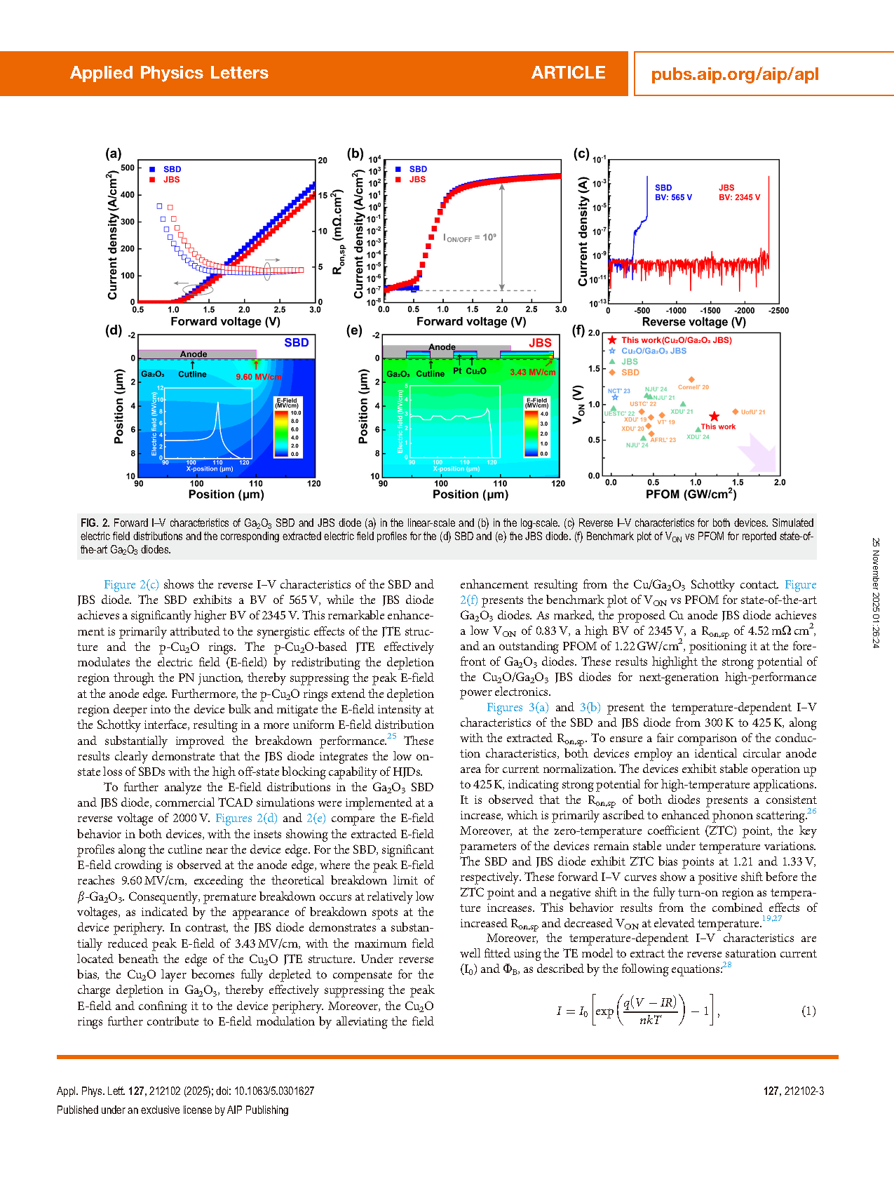
Fig. 2. Forward I–V characteristics of Ga2O3 SBD and JBS diode (a) in the linear-scale and (b) in the log-scale. (c) Reverse I–V characteristics for both devices. Simulated electric field distributions and the corresponding extracted electric field profiles for the (d) SBD and (e) the JBS diode. (f) Benchmark plot of VON versus PFOM for reported state-of-the-art Ga2O3 diodes.
DOI:
10.1063/5.0301627