


Member News
【Member News】Setting the Standard for the Future! Two Gallium Oxide Group Standards Led by Garen Semiconductor Officially Released
日期:2025-12-16阅读:843
Recently, two group standards led by Hangzhou Garen Semiconductor Co., Ltd.—β- Gallium Oxide Homoepitaxial Wafers (T/CEMIA 050-2025) and Test Method for Dislocation Density in Gallium Oxide Single Crystals (T/CEMIA 051-2025)—were officially approved and released by the China Electronic Materials Industry Association. Both standards will come into full effect on January 1, 2026.
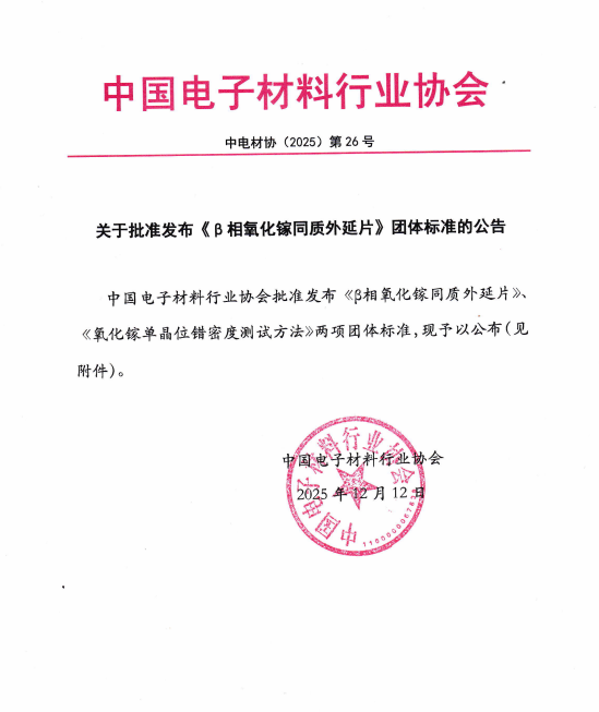
This marks a major breakthrough in China’s standardization efforts for fourth-generation semiconductor materials, signaling a critical step forward for the Gallium Oxide industry from technological research toward large-scale industrial application.
The leading organization for β-Ga₂O₃ Homoepitaxial Wafers (T/CEMIA 050-2025) is Hangzhou Garen Semiconductor Co., Ltd.
Other participating organizations include: the 46th Research Institute of China Electronics Technology Group Corporation (CETC), University of Science and Technology of China, the 13th Research Institute of CETC, Xidian University, Nanjing University, Sun Yat-sen University, Yongjiang Laboratory, Zhejiang University, Zhejiang University Hangzhou International Science and Technology Innovation Center, Hangzhou Fujia Gallium Technology Co., Ltd., Evolution Semiconductor Co., Ltd., Shenzhen Pinghu Laboratory, China Resources Microelectronics Limited, NEXTGO EPI UG, University of Electronic Science and Technology of China, Anhui University, Xiamen University, Suzhou Institute of Nano-Tech and Nano-Bionics (SINANO), Chinese Academy of Sciences, GaFuture Semiconductor Technology (Jinjiang) Co., Ltd., Dalian University of Technology, Dongguan Institute of Materials Science and Technology, Chinese Academy of Sciences, Hubei Jiufengshan Laboratory, Hangzhou Xinchuangde Semiconductor Co., Ltd., Southwest University, and The Hong Kong University of Science and Technology.
The leading organization for Test Method for Dislocation Density in Gallium Oxide Single Crystals (T/CEMIA 051-2025) is also Hangzhou Garen Semiconductor Co., Ltd.
The other participating organizations are the same as those involved in T/CEMIA 050-2025, including major research institutes, universities, laboratories, and industrial partners across China and abroad.
These two Gallium Oxide–related group standards, released by the China Electronic Materials Industry Association, will provide authoritative references for quality control of β-phase Gallium Oxide homoepitaxial wafers and for unified testing of dislocation density in Gallium Oxide single crystals. The implementation of these standards will accelerate the transition of Gallium Oxide from laboratory research to large-scale production, laying a solid foundation for China to establish both technological and industrial advantages in the field of ultra-wide-bandgap semiconductors. This progress will help unlock the industrial value of Gallium Oxide as the “king of ultra-wide-bandgap semiconductors” and support national strategies in new energy and high-end manufacturing.
Note: The above content is sourced from the Semiconductor Materials Industry Branch. Author: Semiconductor Materials Industry Branch.
Original article: “β-Ga₂O₃ Homoepitaxial Wafers” and “Test Method for Dislocation Density in Gallium Oxide Single Crystals” to Be Officially Implemented on January 1, 2026.
About Garen Semiconductor
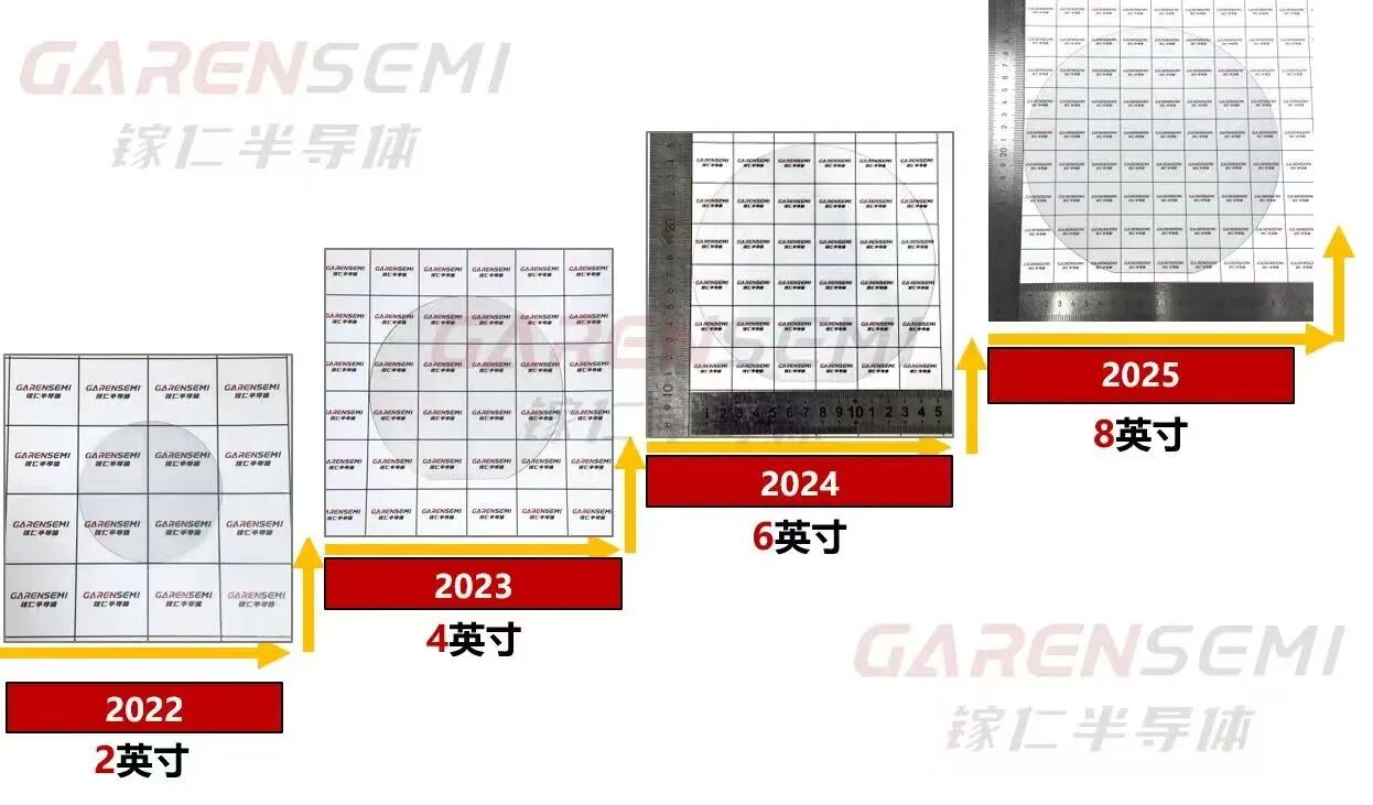
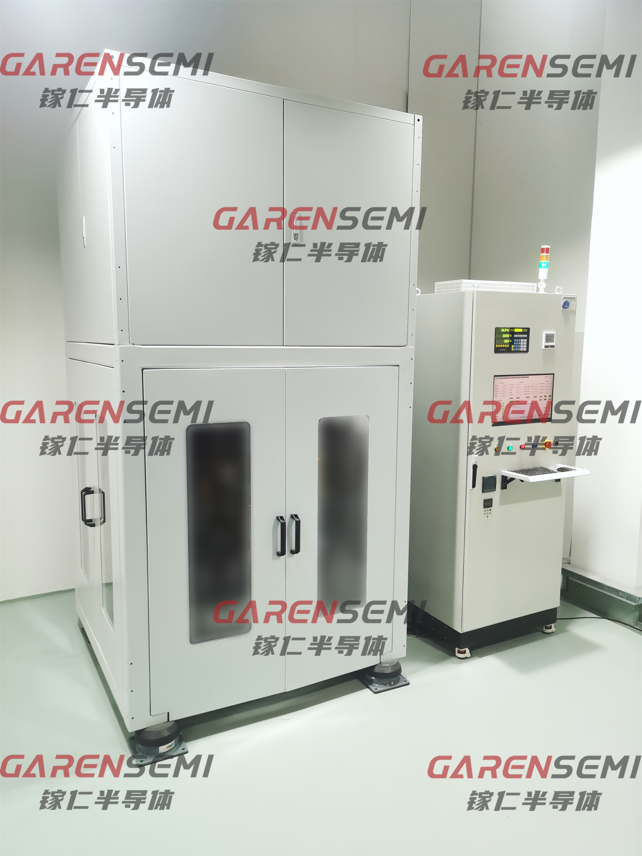
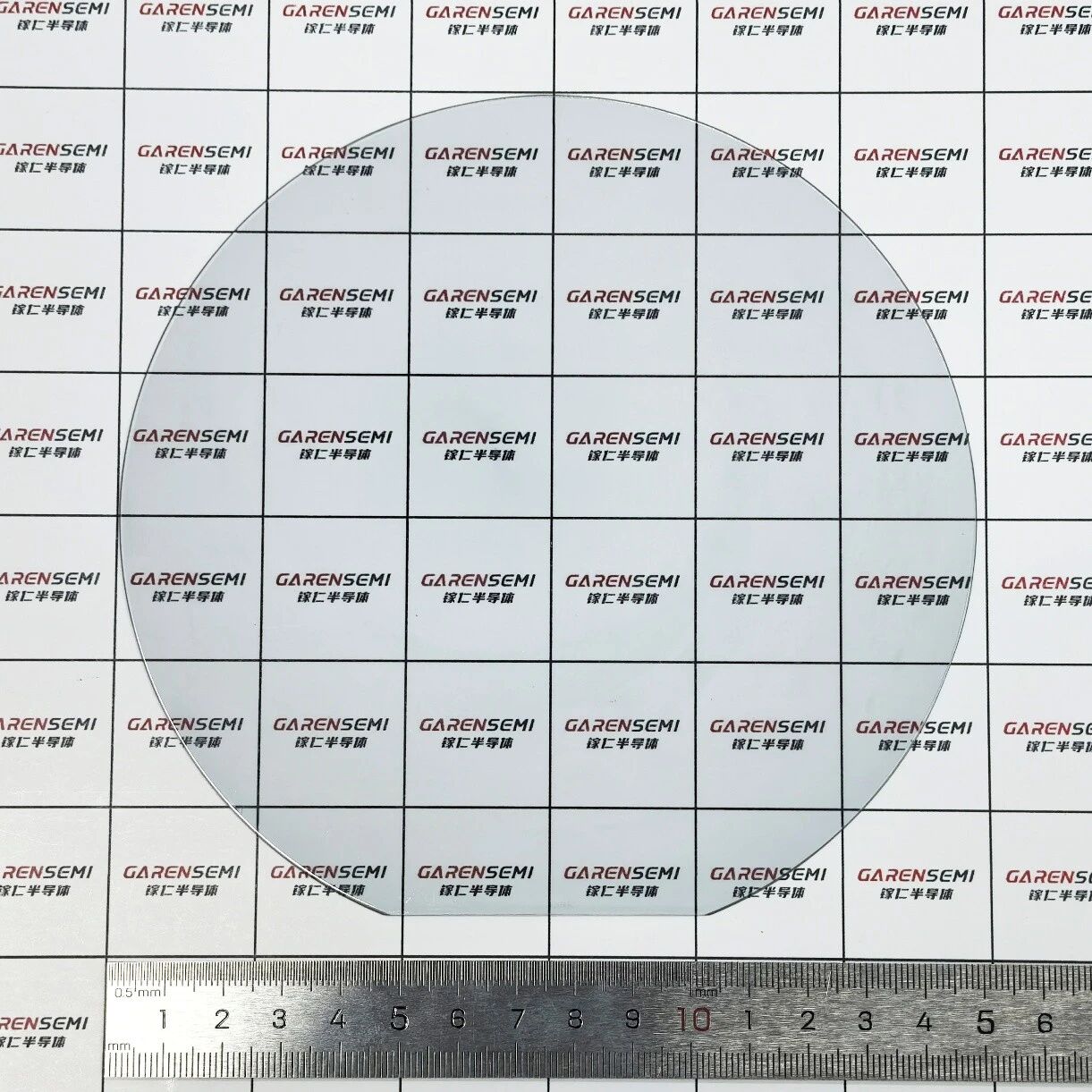
Hangzhou Garen Semiconductor Co., Ltd. is a global leading provider of gallium oxide materials and equipment solutions, dedicated to the research, development, and industrialization of ultra-wide-bandgap semiconductors. The company’s core products include 2–8 inch gallium oxide single crystals and substrates (with 8-inch wafers being a world first), vertical Bridgman (VB) crystal growth equipment for gallium oxide, and gallium oxide epitaxial wafers, all of which are now commercially available.
2–8 inch Gallium Oxide Single Crystals and Substrates
(8-inch wafers: world first)
“SCIENCE Series”
Research-grade VB crystal growth equipment
Gallium Oxide Homoepitaxial Wafers
Garen Semiconductor is committed to building a full-chain product system covering “equipment–crystal–substrate–epitaxy”, providing comprehensive, system-level solutions to customers worldwide. Its achievements in the Gallium Oxide field have been widely reported by major media outlets, including People’s Daily, Xinhua News Agency, Science and Technology Daily, Sina Finance, China Blue News, and The Paper.
Corporate Honors and Achievements
In 2023, the company was recognized as a National Science and Technology–Based SME and a Zhejiang Provincial Innovative SME; in 2024, it was awarded the title of Zhejiang Provincial “Specialized, Refined, Distinctive, and Innovative” SME. In 2025, Garen Semiconductor received multiple honors, including the SEMICON CHINA “SEMI Outstanding Contribution to Sustainability Award”, the Jiufengshan Forum (JFSC) & Compound Semiconductor Industry Expo “Unity and Collaboration Award”, and the Zhejiang Semiconductor Industry “Innovation Vitality Award”; it won Second Prize in the Enterprise Group of the 10th “Maker in China” Zhejiang Provincial Finals, was selected among the Top 500 Enterprises Nationwide in the 10th “Maker in China” SME Innovation and Entrepreneurship Competition, and received the 2024–2025 Semiconductor Materials Industry Contribution Award. The achievement “Major Breakthrough in the Preparation of 8-inch Gallium Oxide Single Crystals and Substrates” was selected as one of the “Top Ten Advances in China’s Third-Generation Semiconductor Technologies (2025)” and as a Major Scientific and Technological Achievement of Zhejiang Province (2025). In addition, the company has led the drafting of two gallium oxide group standards, participated in the formulation of one national standard, and contributed to the promotion of another group standard; it has received support from the “5213” Excellence Program of Xiaoshan District, Hangzhou, and has been granted 13 invention patents (including U.S. and Japanese patents), with more than 50 patent applications filed.
For more information about Garen Semiconductor and its products, please visit our official website:
http://garen.cc/
Or contact us at:
Mr. Jiang: +86 159 1871 9807
Email: jiangjiwei@garen.cc
Mr. Xia: +86 190 1127 8792
Email: xianing@garen.cc
