Paper Sharing
【Member Papers】Robust Ga₂O₃ Memristor with Sharp Stable Negative Differential Resistance for Energy-Efficient Reliable Analog Resistive Switching and Artificial Synapse Applications
日期:2025-12-18阅读:541
Researchers from Gang Xiang Group at Sichuan University have published a paper titled "Robust Ga2O3 Memristor with Sharp Stable Negative Differential Resistance for Energy-Efficient Reliable Analog Resistive Switching and Artificial Synapse Applications" in ACS Nano (DOI:https://doi.org/10.1021/acsnano.5c15821).
Background
Memristors, owing to their simple structure, nonvolatile characteristics, and ability to emulate synaptic behavior, are regarded as a key device platform for next-generation memory and neuromorphic computing. However, under high-electric-field operation or high-density integration, conventional memristors commonly suffer from current overshoot, excessive power consumption, and severe thermal accumulation, which seriously limit device stability and reliability. At present, most memristors still rely on external current-limiting circuits to suppress excessive current, increasing system complexity and reducing overall energy efficiency. Therefore, developing low-power memristors with intrinsic current self-limiting capability and stable operation under high electric fields has become a critical challenge that urgently needs to be addressed.
β-Ga₂O₃, as an ultrawide-bandgap semiconductor, exhibits a high critical breakdown field, excellent thermal stability, and strong radiation hardness, making it an ideal material platform for constructing highly reliable memristors. Nevertheless, achieving effective power regulation and current limitation in β-Ga₂O₃-based memristors under high electric fields remains challenging. The negative differential resistance (NDR) effect, characterized by a decrease in current with increasing voltage, inherently provides current self-clamping capability. However, the introduction and stable realization of NDR in β-Ga₂O₃ memristors have not yet been systematically investigated.
Abstract
Nowadays, memristors mainly rely on external circuits to manage power consumption, especially under high electric fields, which increases system complexity and reduces energy efficiency. To solve this problem, it is desirable to achieve memristors with an intrinsic current-limiting mechanism that can energy-efficiently work under high electric fields. Here, we demonstrate a robust Sn-doped β-Ga2O3 memristor that exhibits a prominent negative differential resistance (NDR) effect at the MV m–1 level, which enables effective self-limiting of overshoot current. The coexistence of the NDR and resistive switching characteristics is attributed to the reversible migration of oxygen vacancies and dynamic modulation of the Schottky barrier. Importantly, the memristor demonstrates record-breaking NDR performance metrics, including the sharpest slope up to 3.55 and the longest endurance up to 103 cycles and 104 seconds, among the reported ones. Furthermore, the memristor exhibits typical analog resistive switching and essential artificial synapse behaviors. Assisted with the sharpest and stablest NDR effect under high electric field, the robust Ga2O3 memristor offers a promising platform toward high-performance energy-efficient multifunctional applications.
Conclusion
In summary, we have demonstrated a robust Sn-doped β-Ga₂O₃ memristor that integrates a sharp and stable negative differential resistance (NDR) effect with analogue resistive switching (RS) and essential artificial synapse (AS) behaviors. The optimized memristor exhibits a prominent NDR effect, featuring the sharpest slope of up to 3.55 and the longest endurance of up to 10³ cycles and 10⁴ s among the reported memristors, thereby providing robust intrinsic current-limiting capability for energy-efficient and reliable applications such as memory storage and neuromorphic computing. Our results provide insight into memristors with the coexistence of NDR–RS–AS characteristics and offer a promising route toward multifunctional applications based on β-Ga₂O₃.
Project Support
This work was supported by the National Key Research and Development Program of China (MOST) . We thank the Analytical & Testing Center of Sichuan University for the SEM, TEM, XPS, and XRD measurements.
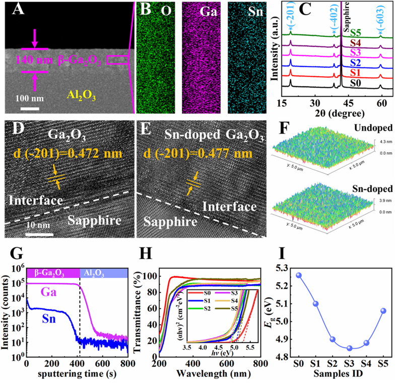
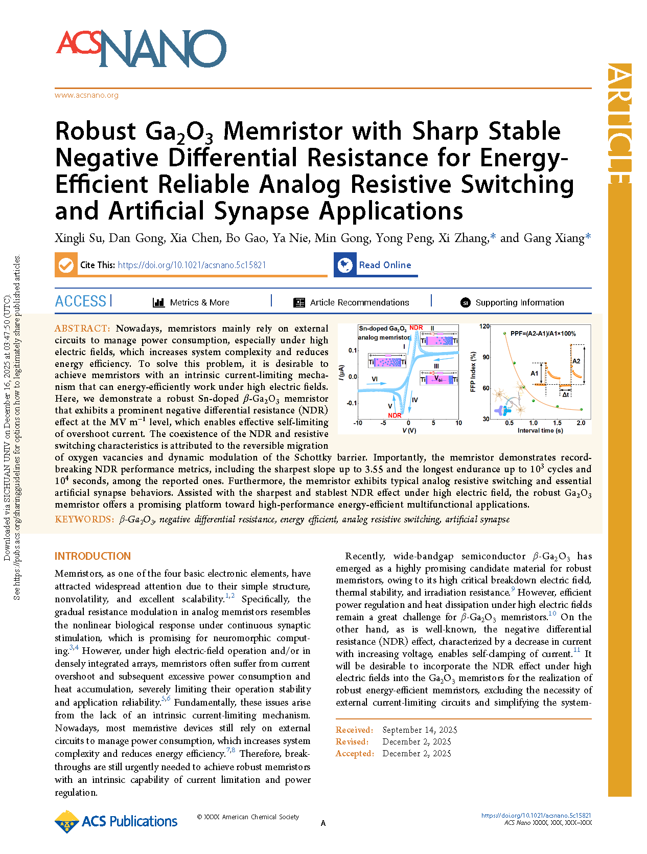
Figure 1.(A) Cross-sectional SEM image and (B) corresponding EDS mapping of S3. (C) XRD patterns of S0–S6. (D, E) Cross-sectional HRTEM images of S0 and S3, respectively.(F) AFM images of S0 (Rq = 0.522 nm) and S3 (Rq = 0.498 nm). (G) SIMS depth profile of Ga and Sn elements in S3. (H) Optical transmittance spectra of S0–S6; the inset shows the (αhν)² versus hν plot. (I) Variation of the bandgap energy (Eg) in S0–S6.
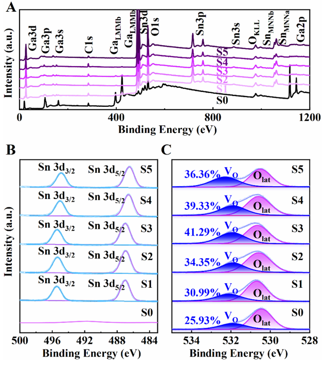
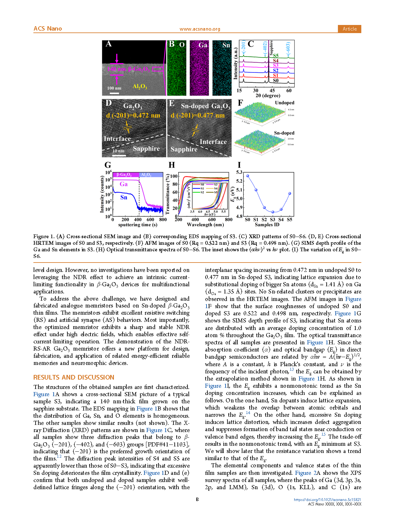
Figure 2. (A) XPS survey spectra, (B) Sn 3d peaks, and (C) O 1s peaks of S0−S5. The integrated area ratios of the VO-related peak are shown in (c).
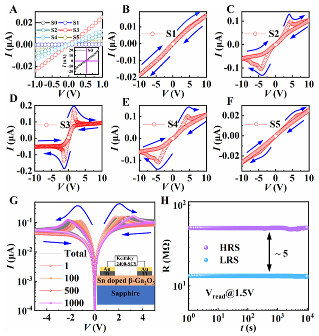
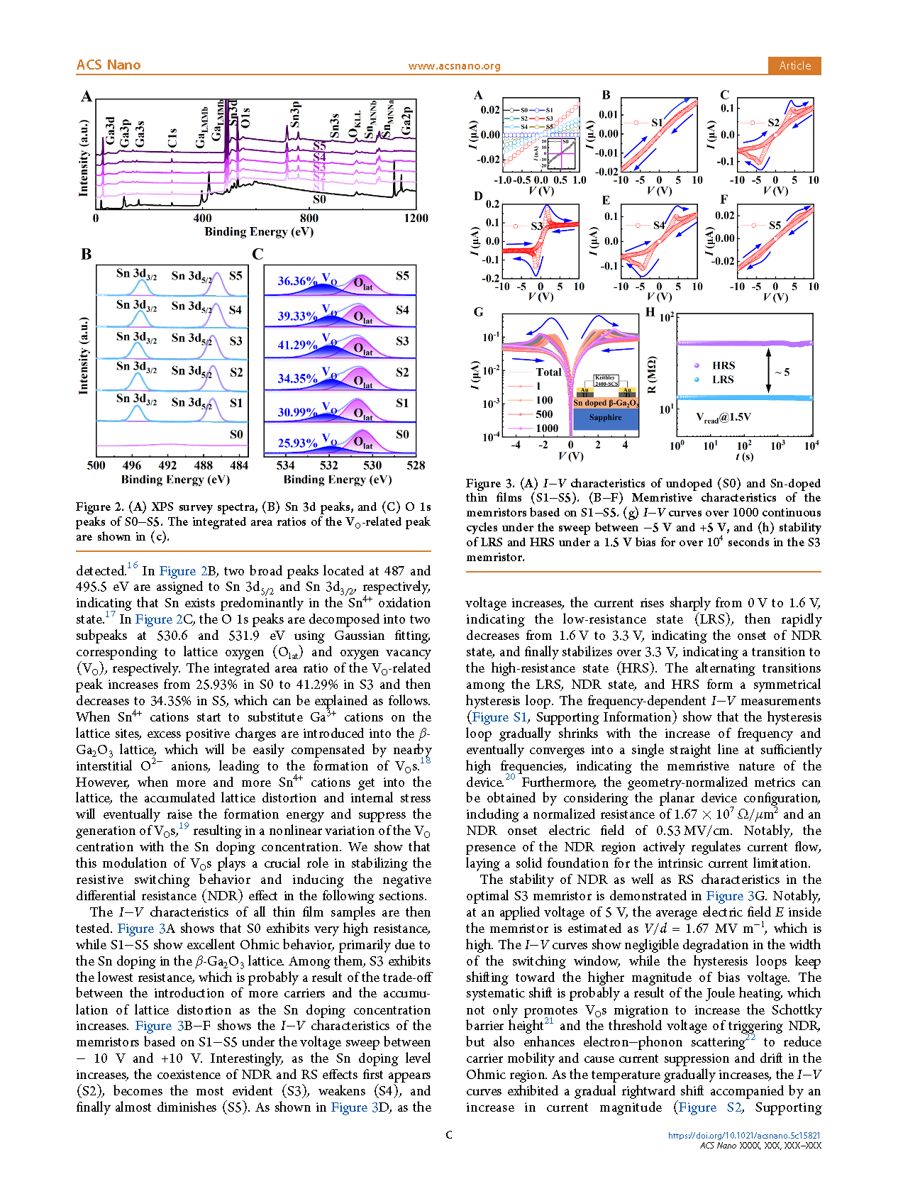
Figure 3. (A) I−V characteristics of undoped (S0) and Sn-doped thin films (S1−S5). (B−F) Memristive characteristics of the memristors based on S1−S5. (g) I−V curves over 1000 continuous cycles under the sweep between −5 V and +5 V, and (h) stability of LRS and HRS under a 1.5 V bias for over 104 seconds in the S3 memristor.
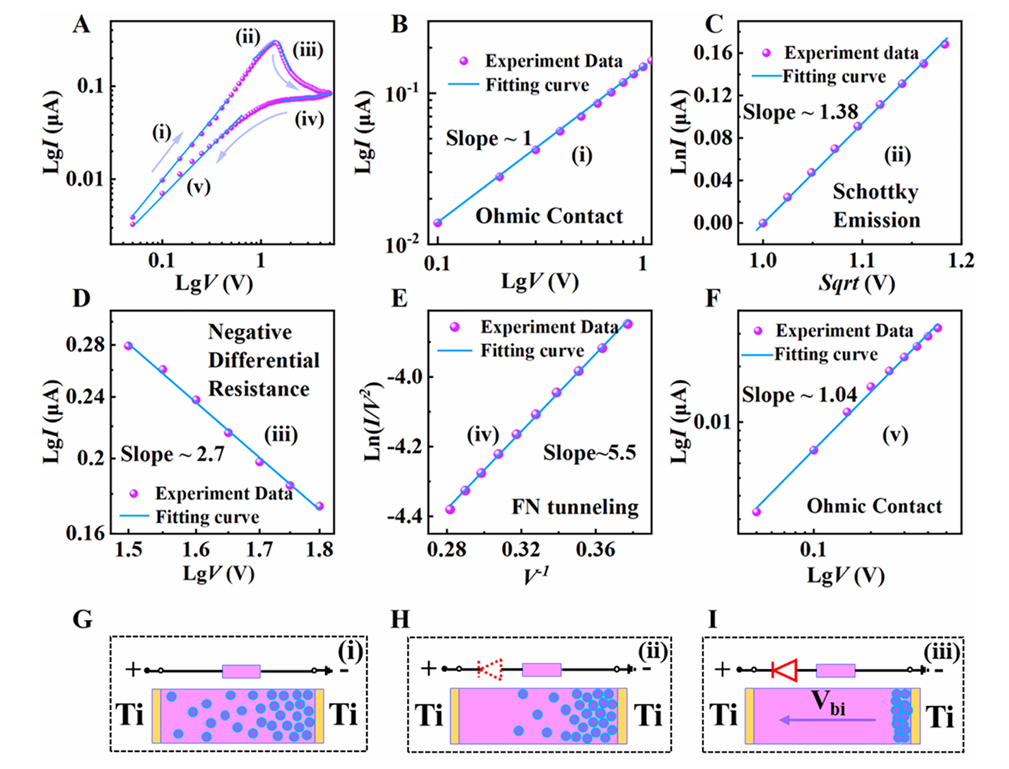
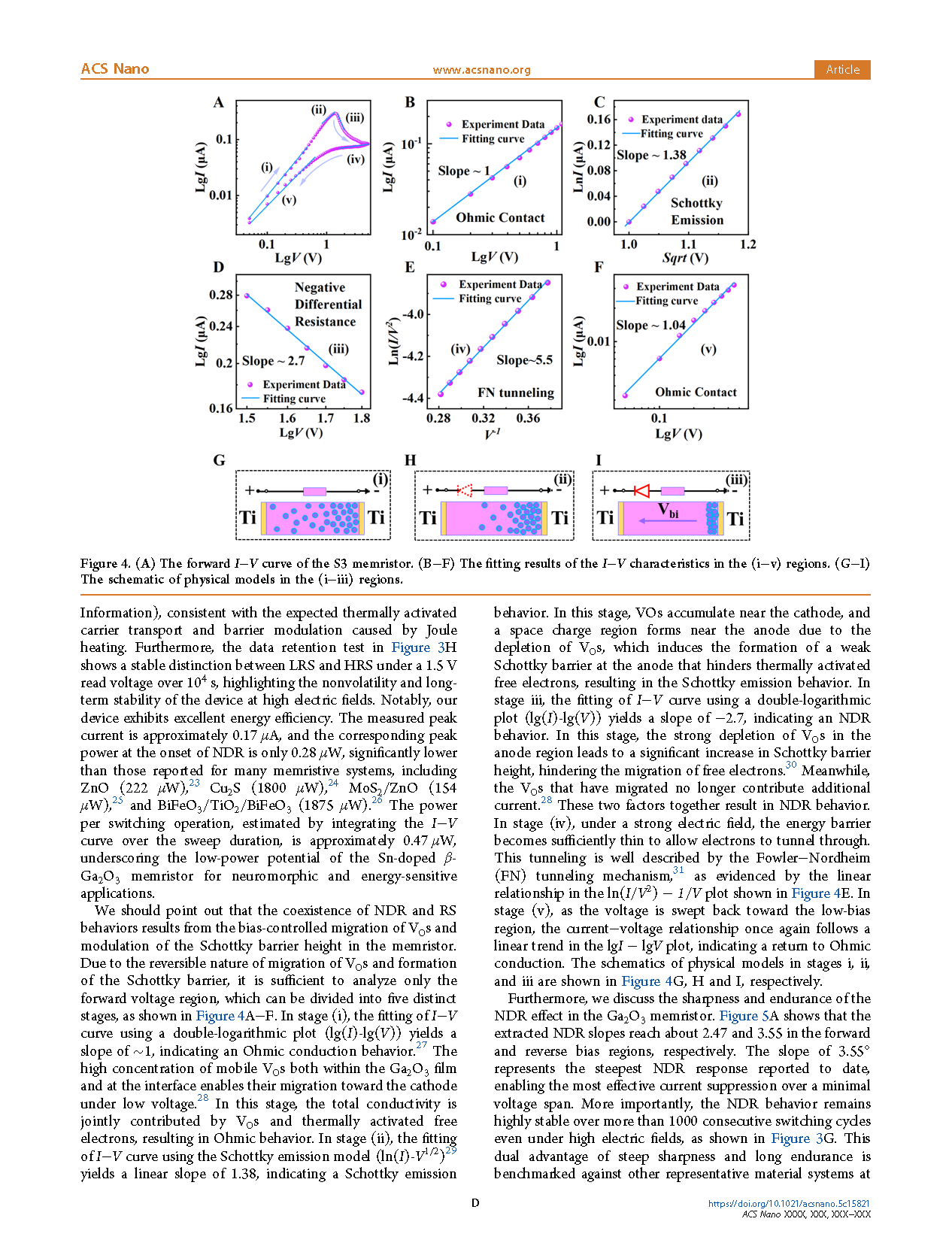
Figure 4.(A) Forward I–V curve of the S3 memristor. (B–F) Fitting results of the I–V characteristics in regions (i–v). (G–I) Schematics of the physical models in regions (i–iii).
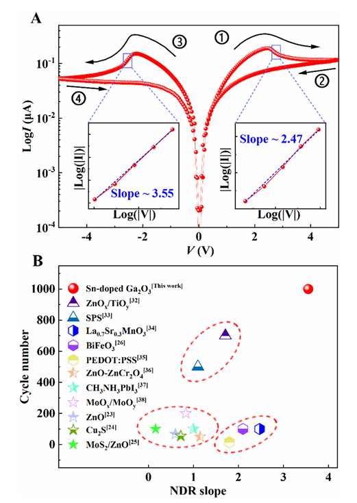
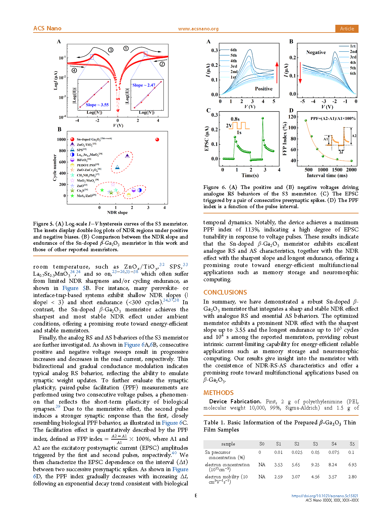
Figure 5. (A) Log-scale I–V hysteresis curves of the S3 memristor. The insets display double-log plots of the NDR regions under positive and negative biases.
(B) Comparison of the NDR slope and endurance of the Sn-doped β-Ga₂O₃ memristor in this work with those of other reported memristors.
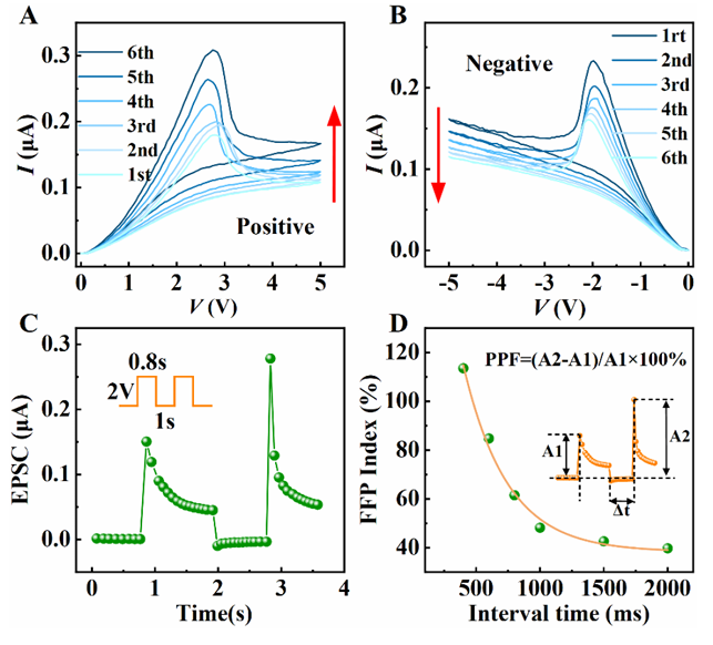
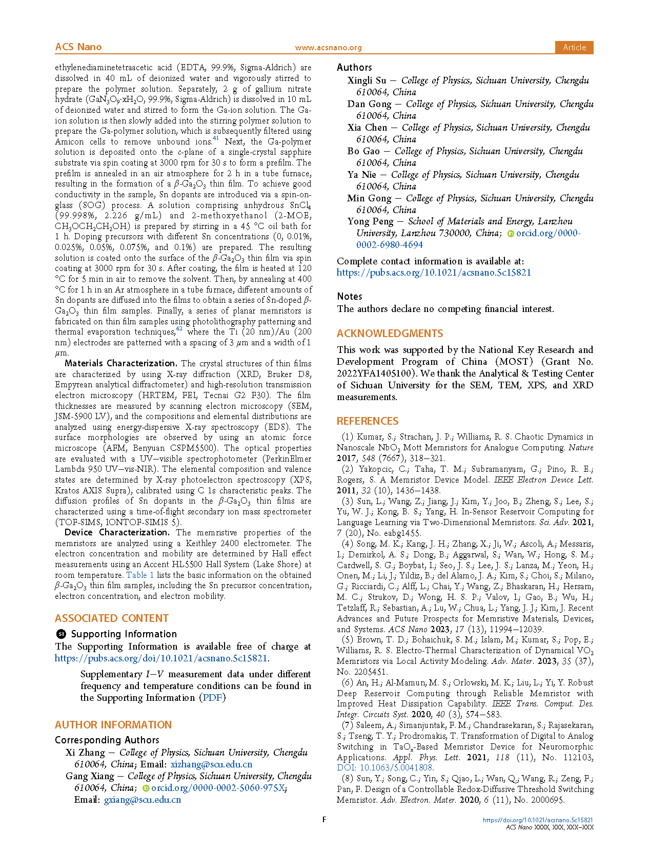
Figure 6. (A) Positive and (B) negative voltages driving analogue RS behaviors of the S3 memristor. (C) EPSC triggered by a pair of consecutive presynaptic spikes. (D) PPF index as a function of the pulse interval.
DOI:
doi.org/10.1021/acsnano.5c15821