Expert Interview
【Expert Interview】Hardcore Technology + Strategic Layout: Chairman Qi Hongji Explains How Fujia Gallium Leads the Gallium Oxide Sector
日期:2025-12-19阅读:1036
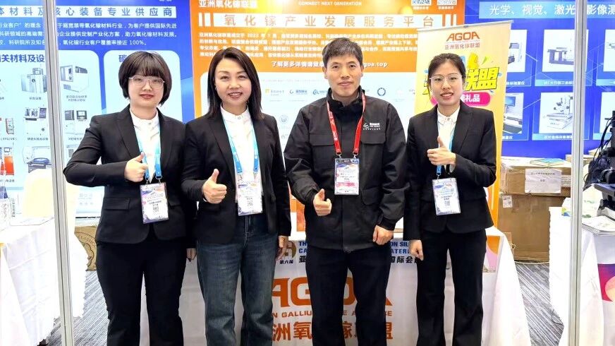
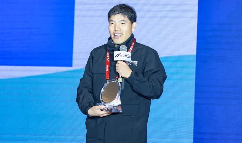
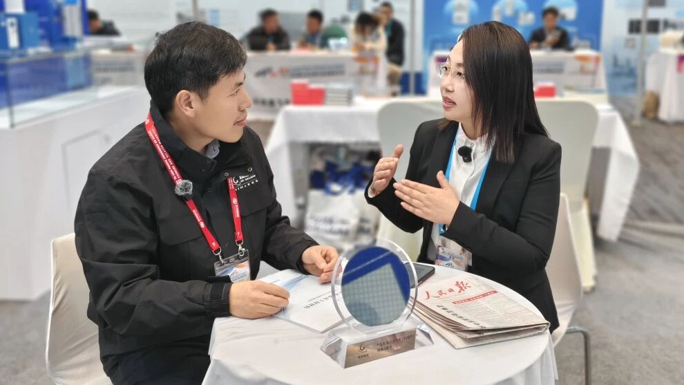
At the 6th Asia Pacific Conference on Silicon Carbide and Related Materials (APCSCRM 2025), Gallium Oxide emerged as one of the key focal points of attention within the industry. As an invited participant, the Alliance conducted a dedicated interview during the conference with Qi Hongji, Chairman of Hangzhou Fujia Gallium Technology Co., Ltd., a governing member of the Alliance, engaging in in-depth discussions on the company’s technological applications and industrialization strategy in the field of Gallium Oxide.
What prompted you to move from laboratory research to industrialization and establish Fujia Gallium?
Our decision to establish Fujia Gallium and bring Gallium Oxide materials from the laboratory into industrial application was the inevitable result of multiple converging factors. I have always remembered my mentor’s guidance: “One generation of materials enables one generation of devices, which in turn drives one generation of applications.” This deeply impressed upon me that breakthroughs in fundamental materials are the root force behind the upgrading of entire industries.
Building on fifteen years of technological accumulation within our team, we clearly recognized the strategic importance of Gallium Oxide as a fourth-generation semiconductor material. At the same time, clear national strategies and pressing industrial demands made us realize that only by transforming technological advantages into industrial strengths could we truly address the bottlenecks in critical materials. The establishment of the Hangzhou Institute of Optics and Fine Mechanics in 2019 provided a platform for the incubation of scientific and technological achievements. All these factors ultimately drove us, with the vision of “bringing high-quality materials to the world,” to take a firm step toward industrialization at the end of 2019.
What irreplaceable support did the Hangzhou Institute of Optics and Fine Mechanics provide during your industrialization process as a platform for technology transfer and incubation?
Entrepreneurship is inherently challenging. Many outstanding entrepreneurs ultimately fall short of their goals, often not because of insufficient technical capability, but because entrepreneurship itself is a comprehensive test. On the one hand, it requires leading a team to tackle technical challenges, push products toward market adoption, and withstand intense market pressures; on the other hand, it demands precise control of pace, ensuring that technological breakthroughs resonate with the trajectory of industry development.
Having long been engaged in scientific research, we were deeply aware of how difficult the “from 0 to 1” breakthrough can be. Only after starting a business did we truly realize that the “from 1 to 10” path of industrialization is even more arduous. This places extremely high demands on an individual’s overall capabilities: not only must one understand technology, but one must also possess leadership skills to guide a large team through the transition from technology to product.
What the Hangzhou Institute of Optics and Fine Mechanics has provided us goes far beyond physical space. It offers comprehensive support in finance, legal affairs, and investment and financing. More importantly, the institute is actively building an optoelectronics industrial ecosystem. Within such a collaborative community, different parties learn from each other, complement each other’s strengths, and promote coordinated development across the industrial value chain, making our path toward industrialization far more stable and resilient.
Fujia Gallium has achieved a breakthrough in the key VB-method technology for 6-inch growth, reaching the threshold for industrialization. Compared with international counterparts, what advantages does this breakthrough offer? What was the most challenging aspect of the process?
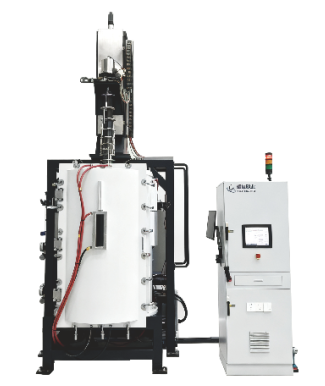
Fujia Gallium has successfully achieved a breakthrough in the VB-method growth technology for 6-inch Gallium Oxide single crystals. The core advantage of this technology lies first in its significant reduction in the use of precious metals, which markedly lowers the one-time capital investment required for equipment in large-scale single-crystal growth, making it more conducive to the industrialization of Gallium Oxide single-crystal substrates. In addition, the crucible-lowering method offers high slicing efficiency per furnace run, further reducing the fabrication cost of single-crystal substrates and accelerating the industrialization of Gallium Oxide substrates.
The central challenge in this breakthrough was the precise control of the temperature field, atmosphere field, and gas-flow field during large-size crystal growth. When the crystal diameter is scaled up to 6 inches, achieving extremely precise and uniform temperature gradients and stress control within a large thermal field becomes exceptionally difficult. Even minor thermal non-uniformities can lead to crystal defects or growth failure. To address this, Fujia Gallium established an independent innovation strategy driven by a “dual-wheel” approach of process and equipment development. Proprietary equipment R&D was carried out in parallel with in-depth optimization of core processes, ultimately overcoming the industrialization challenge of coordinated deterministic thermal-field control and large-size crystal growth. This process constituted a comprehensive test of the team’s interdisciplinary capabilities in materials physics, thermodynamic simulation, and precision manufacturing. Its success marks Fujia Gallium’s establishment of a complete, self-developed technological system spanning from core equipment to mass-production processes.

You have proposed empowering Gallium Oxide industrialization with AI. How does the “one-click crystal growth” equipment address the industry’s reliance on highly specialized talent?
For a long time, the industrialization of new semiconductor materials has been constrained by the heavy dependence of advanced processes on scarce, highly specialized talent, making it difficult to achieve stable, reproducible, and large-scale production.
We clearly recognize that the key to translating laboratory achievements into industry lies in whether the accumulated “experience” of crystal growth can be quantified and transformed into a system that is codifiable, upgradable, and deployable at scale. The “one-click crystal growth” system is precisely the engineering realization of this idea. Through deep integration of artificial intelligence and precision control, it builds a “digital process engineer” that solidifies the human understanding of crystal growth kinetics into an algorithmic core capable of continuous self-optimization, while simultaneously accumulating a valuable data-driven knowledge base for new materials research.
Looking ahead, Fujia Gallium’s “one-click crystal growth” equipment will redefine the process threshold for Fujia Gallium industrialization. It will upgrade materials manufacturing from a model that relies on a small number of veteran experts cultivated over many years to sustain production, to a scalable paradigm of “AI models + deterministic equipment” enabling batch manufacturing.
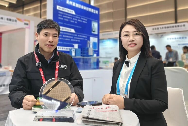
We noticed that during your presentation you were holding a 6-inch vertical Gallium Oxide SBD wafer. What were the key highlights released at the conference this time?
The 6-inch vertical Gallium Oxide Schottky barrier diode (SBD) wafer unveiled at this conference is based on our in-house developed high-mobility homoepitaxial Gallium Oxide wafers and was jointly fabricated with our downstream device partners through a complete tape-out process. The wafer integrates four chip sizes: 3.0 × 3.0 mm², 1.0 × 1.0 mm², 0.5 × 0.5 mm², and φ0.1 mm. During fabrication, an industry-standard 3 mm edge exclusion was adopted, and dicing lanes were reserved for subsequent chip singulation.
The on-site release of the 6-inch vertical Gallium Oxide SBD wafer at the conference marks a significant milestone in Fujia Gallium’s collaboration with downstream device customers, demonstrating active progress in establishing a fully connected technology pathway across the entire Gallium Oxide value chain—from material preparation to large-scale device wafer fabrication. This achievement represents a true industrial leap for Gallium Oxide, transitioning “from availability to usability.” Looking ahead, we will continue to place technological innovation at the core, driving the large-scale deployment of Gallium Oxide devices in a broader range of high-end application scenarios.
Your company has developed in-house MOCVD technology for Gallium Oxide homoepitaxial wafers and carried out device verification. The results indicate that Gallium Oxide shows clear advantages in high-power devices. What is the current device performance?
As an ultrawide-bandgap semiconductor material, Gallium Oxide has demonstrated outstanding performance in high-power devices, which has been extensively verified by research institutions worldwide. Its theoretical performance limits surpass those of silicon carbide, attracting significant attention in the power semiconductor field.
Recently, based on the high-quality thick MOCVD epitaxial wafers provided by our company, a research team from Fuzhou University successfully fabricated high-performance vertical Gallium Oxide power Schottky diodes. Among publicly reported power Schottky diodes fabricated using MOCVD epitaxy, these devices achieved the world’s best PFOM performance (3.07 GW/cm²). From an industrial application perspective, among Gallium Oxide power Schottky diodes reported to date that are fabricated using MOCVD and HVPE epitaxy, the devices demonstrate the best overall performance in terms of the trade-off between turn-on voltage and breakdown voltage. This clearly indicates the excellent quality of the epitaxial wafers produced by our company and their strong supporting role in the further industrialization of Gallium Oxide. This work was peer-reviewed and published in the internationally renowned journal Applied Physics Letters.
China’s Gallium Oxide industry chain has clear advantages in raw materials and application scenarios. How can China achieve international leadership in the field of Gallium Oxide?
China’s Gallium Oxide industry chain enjoys significant advantages in terms of Gallium Oxide raw materials and downstream application scenarios, which constitute the fundamental basis for achieving international leadership in this field. The top priority for realizing such leadership is to rapidly establish a fully connected value chain spanning single crystals, epitaxy, devices, and applications. The key lies in building a collaborative innovation ecosystem that transforms material advantages into product and market advantages. In this process, Fujia Gallium is playing the role of both a “connector” and an “accelerator,” promoting full-chain integration from single crystal to epitaxy, devices, and applications through coordinated advances in technology, capacity, and ecosystem development.
First, at the technological level, we adopt a “dual-wheel drive with collaborative breakthroughs” R&D model. On the materials side, we not only deploy the two internationally recognized technical routes—the Edge-Defined Film-Fed Growth (EFG) method and the Vertical Bridgman (VB) method—but also innovatively establish a coordinated innovation system linking “epitaxial growth and device development.” For example, breakthroughs in MOCVD epitaxy have opened a direct pathway from single-crystal substrates to device fabrication, providing stable raw materials for high-performance power devices and forming a positive technological closed loop from fundamental materials to devices.
Second, in terms of industrialization capability, we are building China’s first 6-inch Gallium Oxide single-crystal and epitaxy production line. This initiative is not only aimed at achieving independent annual production capacity on the order of tens of thousands of wafers, but more importantly at establishing a rapid iteration channel spanning “laboratory research–pilot-scale validation–mass production.” This ensures material stability and quality while significantly shortening device verification and development cycles for downstream partners.
Finally, in ecosystem development, we rely on high-level research platforms to promote deep integration of “industry, education, research, and application.” Upstream, we collaborate with university research teams to tackle fundamental scientific challenges; downstream, we work closely with leading application enterprises to carry out device compatibility development and jointly define product specifications.
Through technological collaboration, platform openness, and ecosystem co-construction, Fujia Gallium is committed to connecting fragmented links in the industry chain into a closed loop and accelerating the transformation of technological value into market value.
Gallium Oxide faces common bottlenecks such as low thermal conductivity and the difficulty of p-type doping. How significant are these issues for industrialization, and what strategies or collaborations has Fujia Gallium pursued to address them?
The low thermal conductivity of Gallium Oxide is an inherent material limitation, and the difficulty of achieving p-type doping is an objective challenge at the current stage of Gallium Oxide development. However, neither low thermal conductivity nor p-type doping difficulty constitutes a fundamental barrier to the industrialization of Gallium Oxide.
From the perspective of thermal management, when combined with state-of-the-art packaging technologies, the drawback of low thermal conductivity can be effectively mitigated. In essence, thermal dissipation is an “engineering problem” that can be addressed through systematic solutions at the device and integration levels.
With regard to the current lack of mature p-type Gallium Oxide, we are pursuing two parallel approaches. On the one hand, we are working with downstream partners to develop MOS device designs based on heterojunction p-type materials or trench structures, enabling the fabrication of high-performance MOS devices even in the absence of p-type Gallium Oxide. On the other hand, we are actively conducting process development for p-type Gallium Oxide epitaxy based on MOCVD technology and have already achieved staged breakthroughs.
Toward the application goal of “tens of kilovolts and kiloampere-level currents,” which technological aspects still require sustained breakthroughs for Gallium Oxide to become both “high-performing” and “cost-effective”?
To achieve the application target of “tens of kilovolts and kiloampere-level currents,” and to ensure that Gallium Oxide is both high-performing and cost-effective, the industry must pursue systematic advances on two fronts simultaneously: overcoming key technical bottlenecks and achieving effective cost control.
On the performance side (“high-performing”), the core challenges lie in pushing beyond intrinsic material limitations. These include addressing the difficulty of p-type doping, mitigating the constraints imposed by low thermal conductivity on high-current operation, and suppressing material defects that degrade device reliability and performance.
On the cost side (“cost-effective”), the key lies in reducing device costs through technological innovation. This involves improving crystal growth efficiency, enabling the growth of larger-diameter ingots, enhancing material quality and utilization efficiency, and minimizing waste. At the same time, strong emphasis must be placed on the development of high-efficiency epitaxial technologies. Through large-scale manufacturing and intelligent process control, superior material performance can be effectively translated into tangible market competitiveness.
Compared with mature semiconductor materials such as silicon carbide and Gallium Nitride, the Gallium Oxide industry currently lacks unified quality evaluation metrics and testing methods. How do you think the industry should accelerate the construction of a standards system?
The lack of a unified quality evaluation system is a critical barrier that must be overcome for the industrialization of Gallium Oxide. The industry should adhere to the principle of “establishing standards driven by application needs, with urgent needs addressed first.” First, key performance indicators should be identified and prioritized as breakthrough points. Second, open testing platforms and data-sharing mechanisms should be established, using large-scale empirical data to provide a solid and reliable basis for standard formulation. Third, a tiered standards system should be built along the full value chain—covering materials, epitaxy, devices, and applications—to ensure that the standards are both forward-looking and practically implementable.
At the same time, active participation in international standardization efforts should be encouraged from the early stages, to help shape rules that reflect both global consensus and China’s industrial interests. At present, Fujia Gallium is taking the lead in promoting the development of national standards in the Gallium Oxide field, working together with the broader industry to lay a solid foundation for large-scale industrialization.
The Shanghai Key Laboratory of Wide-Bandgap and Ultrawide-Bandgap Semiconductor Materials and the Ultrawide-Bandgap Semiconductor Alliance were established in 2025. What value do such industry collaborative organizations bring to accelerating industrialization, and how should enterprises better participate in them?
The establishment of the Shanghai Key Laboratory of Wide-Bandgap and Ultrawide-Bandgap Semiconductor Materials and the Ultrawide-Bandgap Semiconductor Alliance delivers core value by creating a collaborative innovation platform for this strategic industry that efficiently integrates resources across government, industry, academia, research institutes, end users, and capital. This significantly reduces the cost and risk of translating technological achievements from the laboratory to the market. More importantly, such platforms help build consensus across the industrial chain, guide the evolution of technology roadmaps, and lay the groundwork for future industry standards—effectively providing a “fast track” from technological breakthroughs to large-scale applications.
As a leading enterprise in gallium oxide materials, Fujia Gallium has proactively positioned itself as a co-builder of this ecosystem, participating as both a “connector” and a “contributor.” On the one hand, it forms innovation consortia with downstream device companies and research institutions, using application-driven demand to promote coordinated technological breakthroughs. On the other hand, it actively partners with leading end users in fields such as new energy vehicles and smart grids to carry out demonstration applications, enabling rapid iteration of material performance in real-world scenarios. Looking ahead, Fujia Gallium aims not only to accelerate its own development through industrial collaboration, but also to translate its technological practices into industry consensus, actively participate in standards development, and help build an open, win–win industrial ecosystem.
Professor Qi, as a council member of the Alliance, what suggestions do you have for the Alliance’s future development in 2026?
As a council member of the Asian Gallium Oxide Alliance, I have clearly felt the Alliance’s rapid and visible growth. It has played an important role in building consensus, showcasing achievements, and driving overall industry development.
At present, the Alliance’s efforts in deepening collaboration and building a comprehensive ecosystem are still at an early stage. Looking to the coming year, I hope the Alliance can take the lead in organizing cross-border members to jointly explore regional technical specifications for key testing methods of Gallium Oxide materials, while actively promoting the development of international standards in the Gallium Oxide field, thereby helping to build a globally connected industrial ecosystem.