Paper Sharing
【Domestic Papers】High-quality β-(AlₓGa₁₋ₓ)₂O₃ heteroepitaxy grown on (010) Ga₂O₃ via MOCVD and transistor demonstration
日期:2025-12-19阅读:567
Researchers from the University of Science and Technology of China have published a dissertation titled " High-quality β-(AlxGa1-x)2O3 heteroepitaxy grown on (010) Ga2O3 via MOCVD and transistor demonstration" in Semiconductor Science and Technology.
Background
β-Ga₂O₃, as an emerging ultra-wide-bandgap semiconductor, features a 4.8 eV bandgap, an 8 MV/cm critical breakdown field, and an extremely high Baliga’s figure of merit, making it a highly promising material for next-generation high-power, low-loss electronic devices. By introducing Al₂O₃ to form the (AlₓGa₁₋ₓ)₂O₃ alloy, the bandgap can be increased to 8.8 eV, and the theoretical breakdown field can reach 16 MV/cm, further enhancing device voltage-blocking capability. Current research mainly focuses on β-(AlₓGa₁₋ₓ)₂O₃/β-Ga₂O₃ epitaxy and 2DEG structures. However, high-voltage power devices based on uniformly doped (AlₓGa₁₋ₓ)₂O₃ epitaxial films remain relatively rare. In this work, high-quality β-(AlₓGa₁₋ₓ)₂O₃ epitaxy was realized on (010) β-Ga₂O₃ substrates using MOCVD, and for the first time, a MOSFET based on this epitaxial film was demonstrated, exhibiting a breakdown voltage exceeding 3000 V. This result confirms the significant potential of (AlₓGa₁₋ₓ)₂O₃ for high-voltage power electronic applications.
Abstract
This work demonstrates the heteroepitaxial growth of single-phase β-(AlₓGa₁₋ₓ)₂O₃ on (010) β-Ga₂O₃ substrates via metalorganic chemical vapor deposition (MOCVD), achieving an aluminum composition of up to 22.6% with no phase segregation characterized by X-Ray Diffractometer (XRD). The surface morphology of epitaxial layer becomes rougher initially and then smoother with the increase of Al composition, suggesting that the rising Al composition leads to changes in the epitaxial growth mode. The fabricated MOSFETs based on β-(Al0.09Ga0.91)2O3 epitaxial film achieve an ultra-high breakdown voltage over 3000 V and a high average breakdown field of 2.3 MV/cm. This work underscores the potential of β-(AlₓGa₁₋ₓ)₂O₃ heteroepitaxy technique and showcases its suitability for high-voltage power device applications.
Conclusion
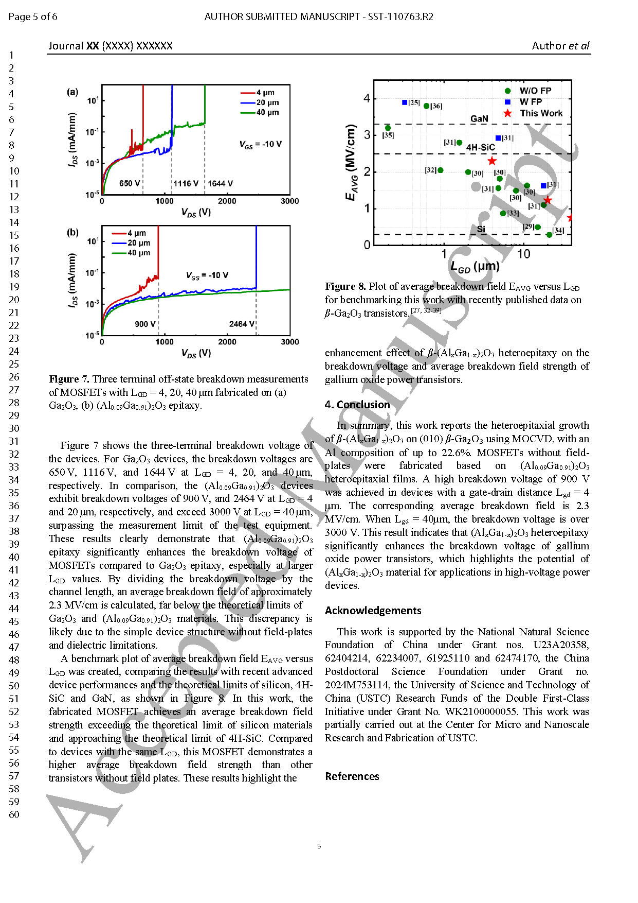
In summary, this work reports the heteroepitaxial growth of β-(AlxGa1-x)2O3 on (010) β-Ga₂O₃ using MOCVD, with an Al composition of up to 22.6%. MOSFETs without fieldplates were fabricated based on (Al0.09Ga0.91)2O3 heteroepitaxial films. A high breakdown voltage of 900 V was achieved in devices with a gate-drain distance Lgd = 4 μm. The corresponding average breakdown field is 2.3 MV/cm. When Lgd = 40μm, the breakdown voltage is over 3000 V. This result indicates that (AlxGa1-x)2O3 heteroepitaxy significantly enhances the breakdown voltage of gallium oxide power transistors, which highlights the potential of (AlxGa1-x)2O3 material for applications in high-voltage power devices.
Project Support
This work is supported by the National Natural Science Foundation of China under Grant nos. U23A20358, 62404214, 62234007, 61925110 and 62474170, the China Postdoctoral Science Foundation under Grant no. 2024M753114, the University of Science and Technology of China (USTC) Research Funds of the Double First-Class Initiative under Grant No. WK2100000055. This work was partially carried out at the Center for Micro and Nanoscale Research and Fabrication of USTC.
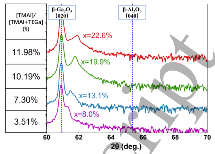
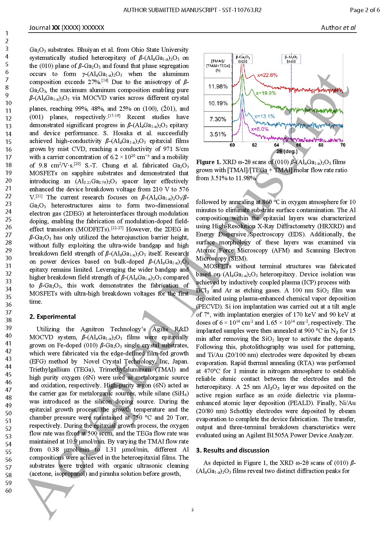
Figure 1. XRD ω-2θ scans of (010) β-(AlₓGa₁₋ₓ)₂O₃ films grown with [TMAl]/[TEGa + TMAl] molar flow rate ratio from 3.51% to 11.98%.

Figure 2. Surface view SEM images of β-(AlₓGa₁₋ₓ)₂O₃ films with Al composition from 8.0% to 22.6%.

Figure 3. The surface AFM images of β-(AlₓGa₁₋ₓ)₂O₃ films with Al composition from 8.0% to 22.6%.
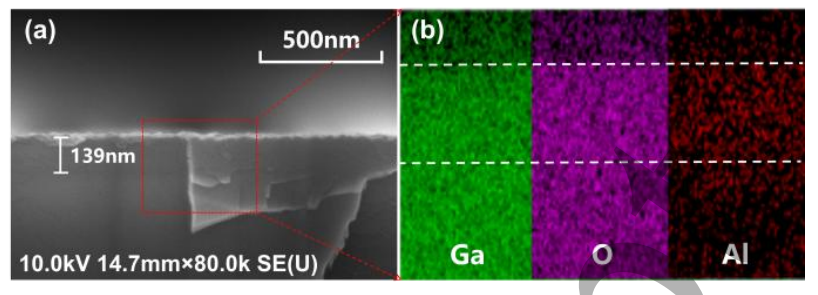
Figure 4. (a) Cross-section SEM view of the β-(Al₀․₁₉Ga₀․₈₁)₂O₃/β-Ga₂O₃ heterostructure. (b) Cross-sectional EDS image of β-(Al₀․₁₉Ga₀․₈₁)₂O₃ film.

Figure 5. Schematic cross section of the β-(AlₓGa₁₋ₓ)₂O₃ MOSFETs without field plates.
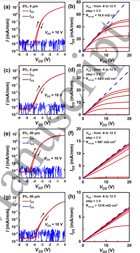
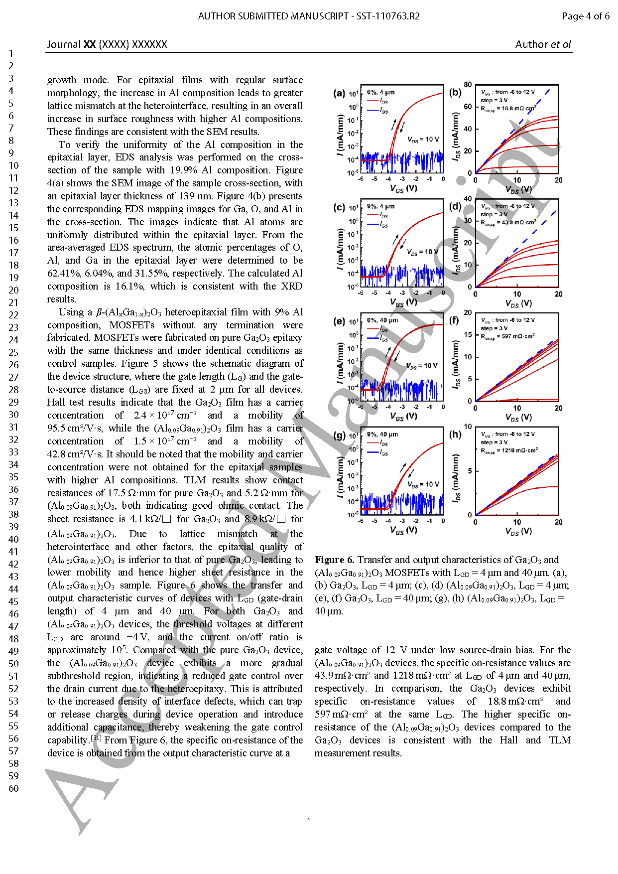
Figure 6. Transfer and output characteristics of Ga₂O₃ and (Al₀․₀₉Ga₀․₉₁)₂O₃ MOSFETs with LGD = 4 μm and 40 μm. (a), (b) Ga₂O₃, LGD = 4 μm; (c), (d) (Al₀․₀₉Ga₀․₉₁)₂O₃, LGD = 4 μm; (e), (f) Ga₂O₃, LGD = 40 μm; (g), (h) (Al₀․₀₉Ga₀․₉₁)₂O₃, LGD = 40 μm.
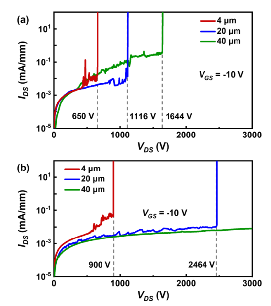
Figure 7. Three terminal off-state breakdown measurements of MOSFETs with LGD = 4, 20, 40 μm fabricated on (a) Ga₂O₃, (b) (Al₀․₀₉Ga₀․₉₁)₂O₃ epitaxy.
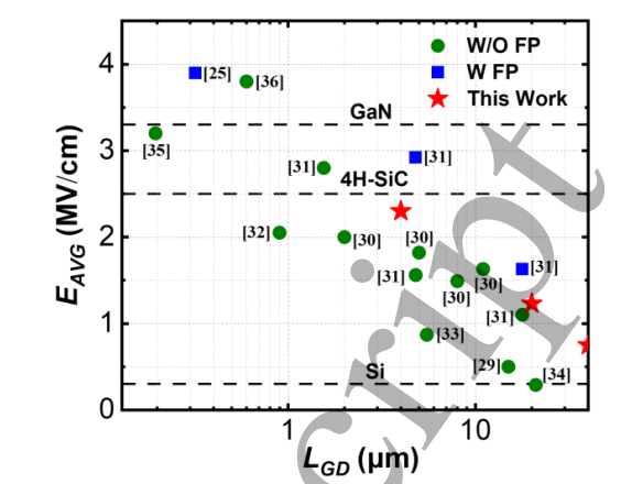
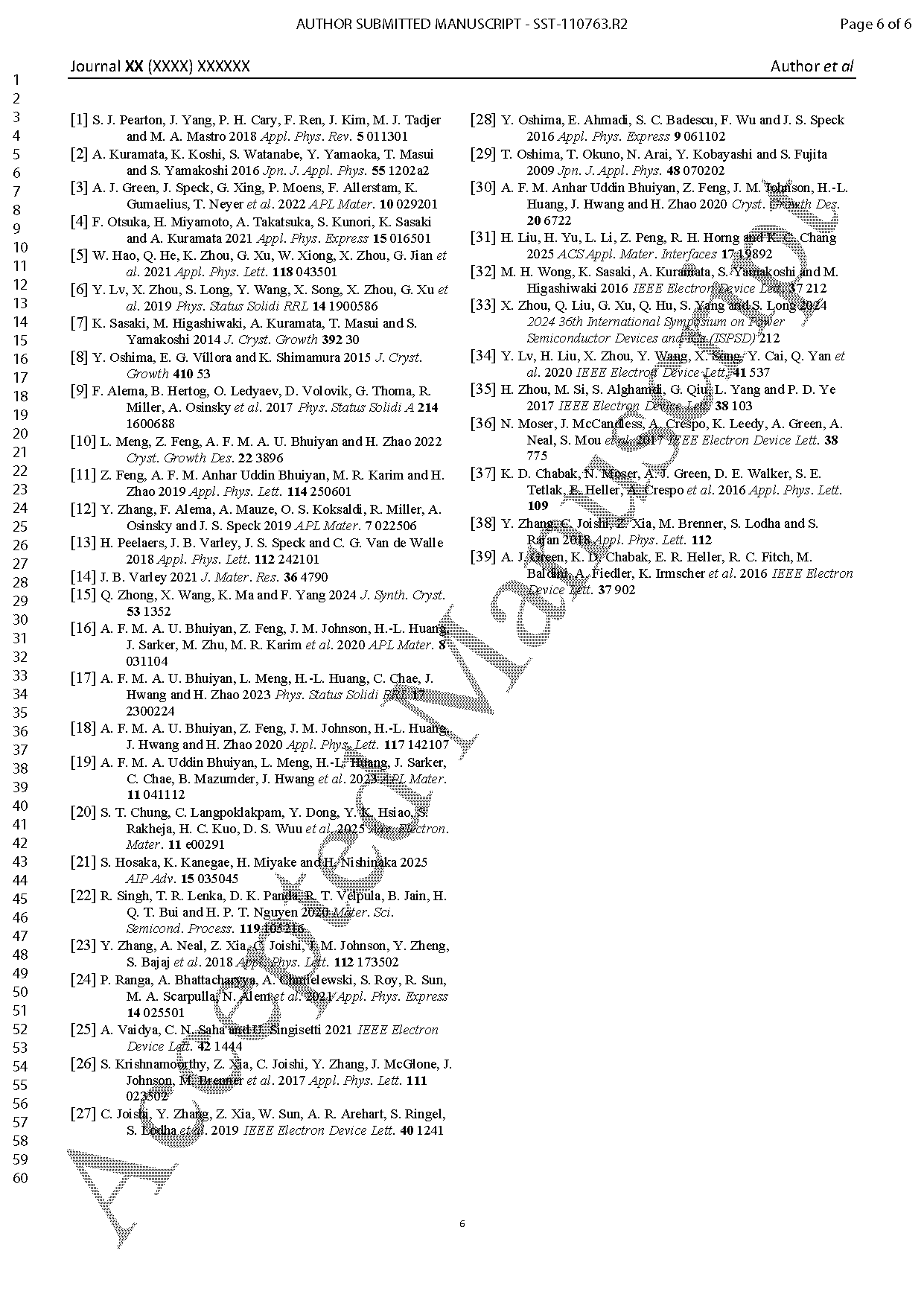
Figure 8. Plot of average breakdown field EAVG versus LGD for benchmarking this work with recently published data on β-Ga₂O₃ transistors.
DOI:
doi.org/10.1088/1361-6641/ae26c3