Paper Sharing
【Domestic Papers】32 ×32 β-Ga₂O₃ MOS solar-blind ultraviolet detector array and its properties
日期:2025-12-19阅读:644
Researchers from the Xi’an University of Posts and Telecommunications have published a dissertation titled "32 ×32 β-Ga2O3 MOS solar-blind ultraviolet detector array and its properties " in Science China-Information Sciences.
Project Support
This work was supported by Natural Science Basic Research Program of Shanxi Province of China (Grant No. 2023-JC-YB-574) and National Natural Science Foundation of China (Grant No. 62304178).
Background
Ga2O3 has an ultra-wide bandgap of 4.5–5.3 eV and is an ideal solar-blind ultraviolet (SUV) detection material. With the surge in demand for image sensors with different wavelength sensing capabilities for machine vision applications based on artificial intelligence, Ga2O3 SUV detection has begun to expand from a single detector to a multi detector imaging array. At present, most studies on Ga2O3 array detectors are based on a metal-semiconductor-metal (MSM) structure.
Abstract
However, this relatively simple structure is susceptible to the persistent photoconductivity (PPC) effect because it lacks an active switching function during the illumination process. Similar to the Si-gate FET, the metal oxide semiconductor (MOS) FET suppresses PPC via gate control. Compared with the Si-gate FET, the MOSFET is easier to integrate into large-scale arrays. Nonetheless, some problems remain unsolved with regard to the preparation process and physical characteristics. As a result, the progress of large-scale Ga2O3 MOSFET detector arrays has been slow. In this study, a 32 × 32 β-Ga2O3 MOSFET SUV detector array was prepared. The photoelectric characteristics, gate-controlled reset function, and imaging performance of the array were analyzed in detail, and the relevant physical mechanism was determined.
Conclusion
A 32 × 32 β-Ga2O3 MOSFET SUV detector array was fabricated. For VG = 2 V/VD = 2 V, the PDCR of the device reached an optimal value of 3 × 10³, and its τr and τd were 62 and 89 ms, respectively. For VG = −10 V, the current suppression ratio of the device increased to 7.7 × 10⁵. Under a 1 kHz gate square wave pulse, the gate-controlled reset response times decreased to the microsecond range (τu = 32 µs, τf = 45 µs). An imaging system was constructed to evaluate the array performance. Using this system, clear imaging results were obtained under SUV illumination. This work is expected to be helpful for advancing the development of Ga2O3 MOSFET SUV image sensors.

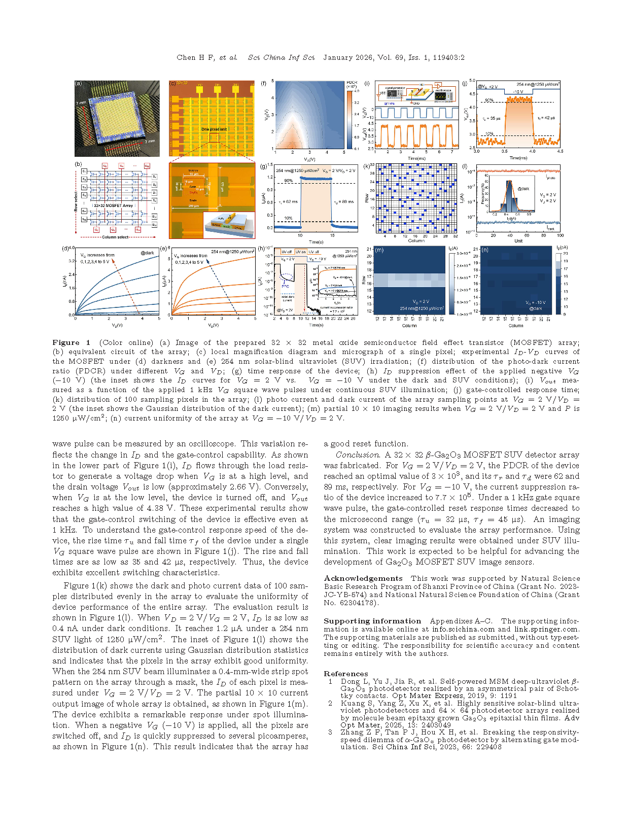
Figure 1 (a) Image of the prepared 32 × 32 metal oxide semiconductor field effect transistor (MOSFET) array; (b) equivalent circuit of the array; (c) local magnification diagram and micrograph of a single pixel; experimental ID-VD curves of the MOSFET under (d) darkness and (e) 254 nm solar-blind ultraviolet (SUV) irradiation; (f) distribution of the photo-dark current ratio (PDCR) under different VG and VD; (g) time response of the device; (h) ID suppression effect of the applied negative VG (−10 V) (the inset shows the ID curves for VG = 2 V vs. VG = −10 V under the dark and SUV conditions); (i) Vout measured as a function of the applied 1 kHz VG square wave pulses under continuous SUV illumination; (j) gate-controlled response time; (k) distribution of 100 sampling pixels in the array; (l) photo current and dark current of the array sampling points at VG = 2 V/VD = 2 V (the inset shows the Gaussian distribution of the dark current); (m) partial 10 × 10 imaging results when VG = 2 V/VD = 2 V and P is 1250 µW/cm2 ; (n) current uniformity of the array at VG = −10 V/VD = 2 V.
DOI:
doi.org/10.1007/s11432-025-4506-1