Paper Sharing
【Domestic Papers】High gain Ga₂O₃/GaN avalanche photodetector with separated absorption and multiplication structure
日期:2025-12-22阅读:634
Researchers from the Jilin University have published a dissertation titled "High gain Ga2O3/GaN avalanche photodetector with separated absorption and multiplication structure" in Applied Physics Letters.
Background
As an emerging ultra-wide bandgap semiconductor material, gallium oxide (Ga2O3) exhibits strong photoresponse properties in the solar-blind ultraviolet (UV) region (200–280 nm) due to its corresponding bandgap of 4.9 eV. Furthermore, Ga2O3 has high optical transparency, an ultrahigh breakdown electric field (8 MV/cm), and excellent thermal stability. These specific characteristics make Ga2O3 have great application potential in solar-blind UV photodetectors (PDs). Among all polymorphs, the β-phase Ga2O3 is widely recognized as the most thermodynamically stable crystalline phase. Among the various types of β-Ga2O3-based PDs that have been researched, avalanche photodetectors (APDs) have more advantages in detecting weak solar-blind signals due to the avalanche multiplication effect. The PN junction is the important component of APD because it can provide a sufficiently high electric field to achieve avalanche multiplication. However, practical p-type Ga2O3 films have not been obtained yet, and Ga2O3-based APDs can only be fabricated based on PN heterojunctions or Schottky barrier junctions.
Abstract
The β-Ga2O3/p-GaN heterojunction avalanche photodetector (APD) with separated absorption and multiplication (SAM) structure was fabricated by metal–organic chemical vapor deposition. Through x-ray diffraction and scanning electron microscopy characterization, the Ga2O3 films exhibit relatively high crystalline quality. Through reasonable design of the electron concentration and thickness of the Ga2O3 layers, the device achieves an ultrahigh avalanche gain (Gain) of 1.75 × 10⁷, an external quantum efficiency (EQE) of 4.53 × 10⁷%, and a high responsivity (R) of 9.28 × 10⁴ A/W under 254 nm solar-blind ultraviolet illumination (5 μW/cm2). The working mechanism of SAM-APD was further validated through TCAD simulations. Compared to conventional APDs, the SAM structure can significantly enhance avalanche gain and EQE, thereby improving the weak signal detection level of the APD effectively.
Conclusion
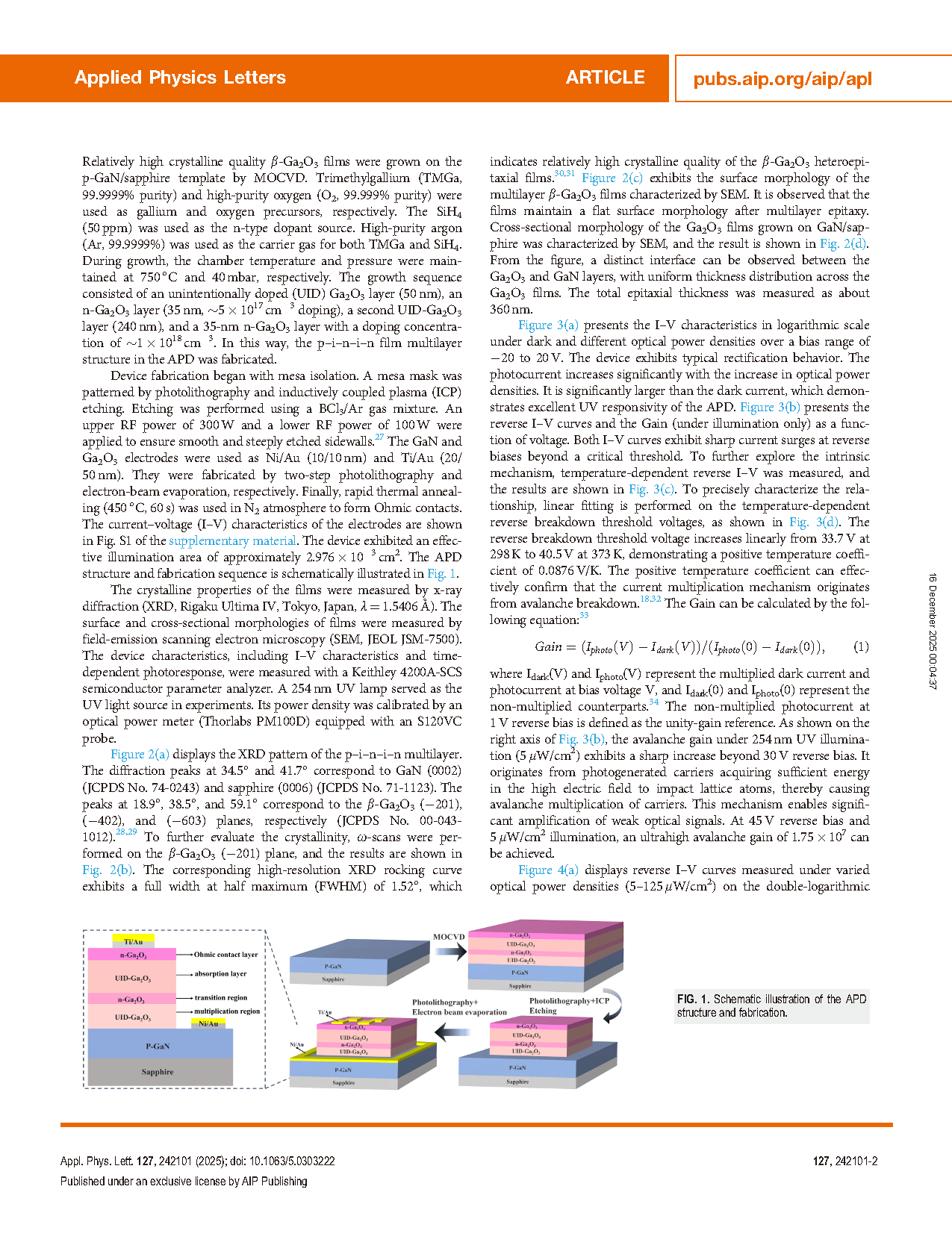
In summary, the solar-blind SAM-APD based on Ga2O3/GaN heterojunction was fabricated by MOCVD. The XRD measurement demonstrated a (-201) orientation and relatively high crystalline quality of Ga2O3 multilayer films. The surface measurement of SEM showed the multilayer films maintain a smooth morphology. The avalanche threshold voltage under dark conditions was found to be approximately -33.7V. Through reasonable design of the electron concentration and thickness of the Ga2O3 layers, the SAM-APD achieved an ultrahigh Gain of 1.75 × 10⁷ , an ultrahigh EQE of 4.53 × 10⁷ %, and a high R of 9.28 × 10⁴ A/W under 254 nm solar-blind UV illumination (5 μW/cm2 ). The gain mechanism of the APD was analyzed by TCAD simulations. The hole-dominated avalanche mechanism circumvents the inherent disadvantage of low hole mobility in Ga2O3 greatly. The SAM structure not only maintains efficient light absorption but also reduces carrier scattering and recombination. Compared to traditional APDs, the APD with SAM structure can operate at a lower working voltage, leading to lower power consumption and higher avalanche gain.
Project Support
This research was funded by the National Key Research and Development Program (Grant No. 2022YFB3605500).
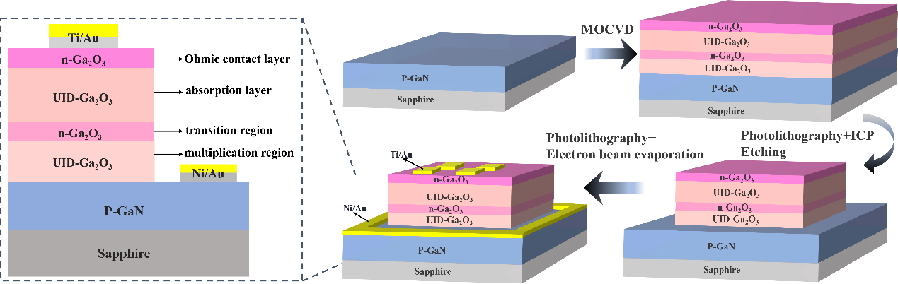
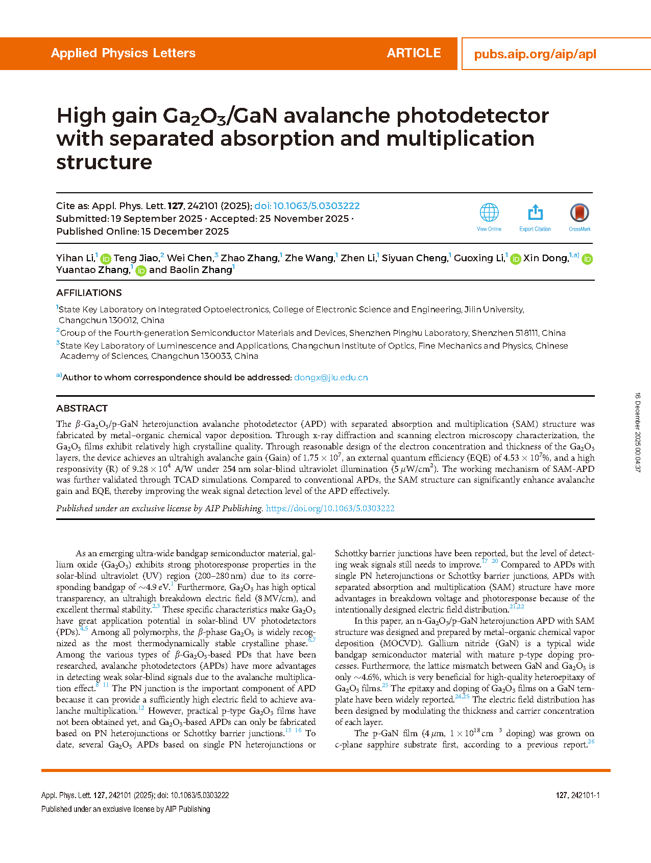
FIG. 1. Schematic illustration of the APD structure and fabrication.
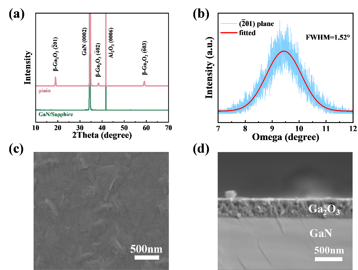
FIG. 2. Characterization of heteroepitaxial Ga2O3 on GaN/sapphire. (a) XRD curve of 2θ-ω scan, (b) rocking curve of the (-201) plane, (c) SEM surface morphology image, and (d) SEM cross-sectional image.
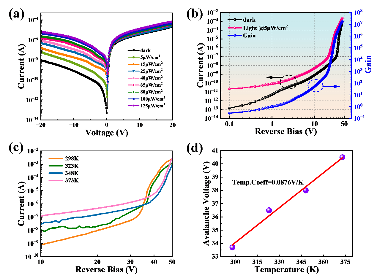
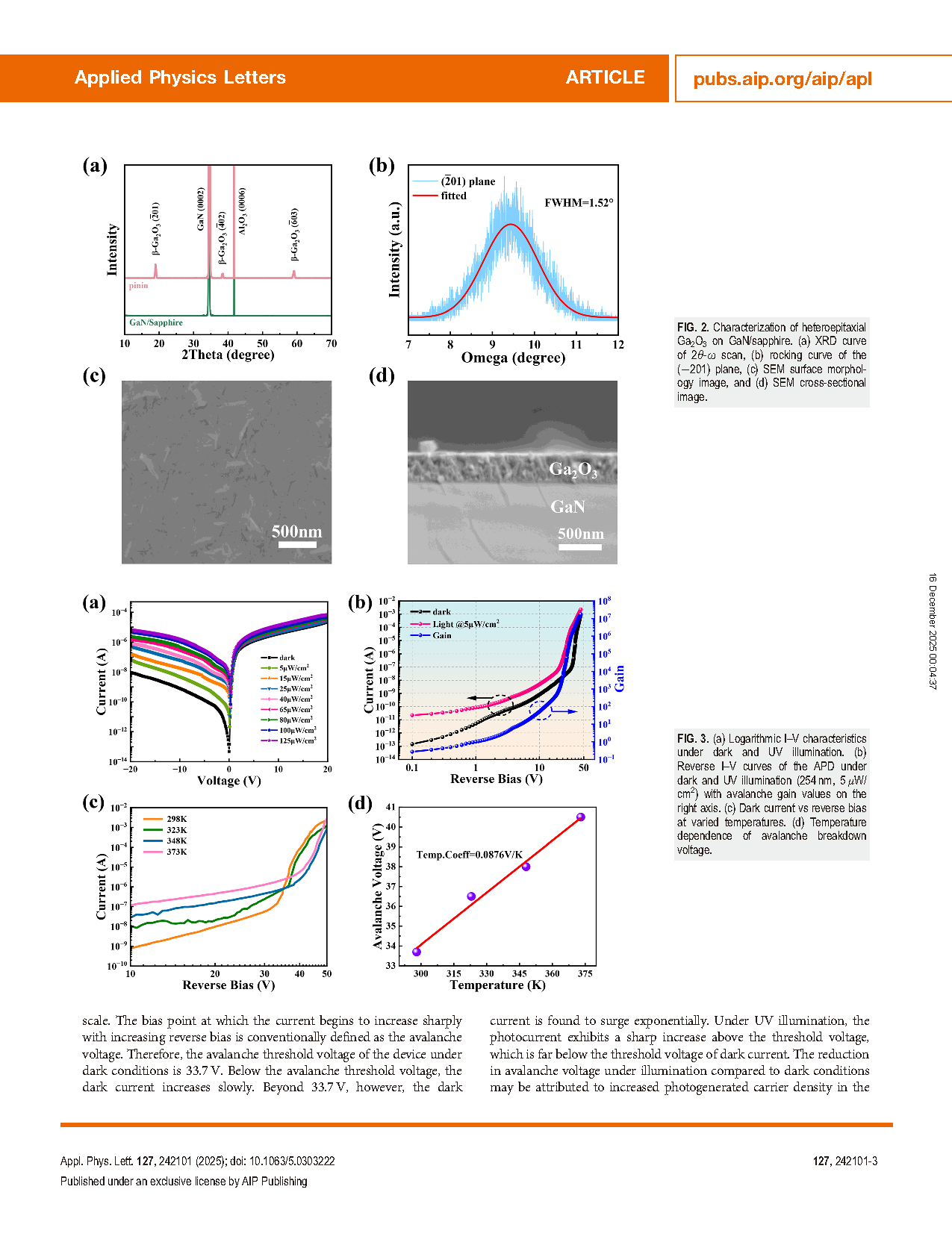
FIG. 3. (a) Logarithmic I–V characteristics under dark and UV illumination. (b) Reverse I–V curves of the APD under dark and UV illumination (254 nm, 5 μW/ cm2) with avalanche gain values on the right axis. (c) Dark current vs reverse bias at varied temperatures. (d) Temperature dependence of avalanche breakdown voltage.
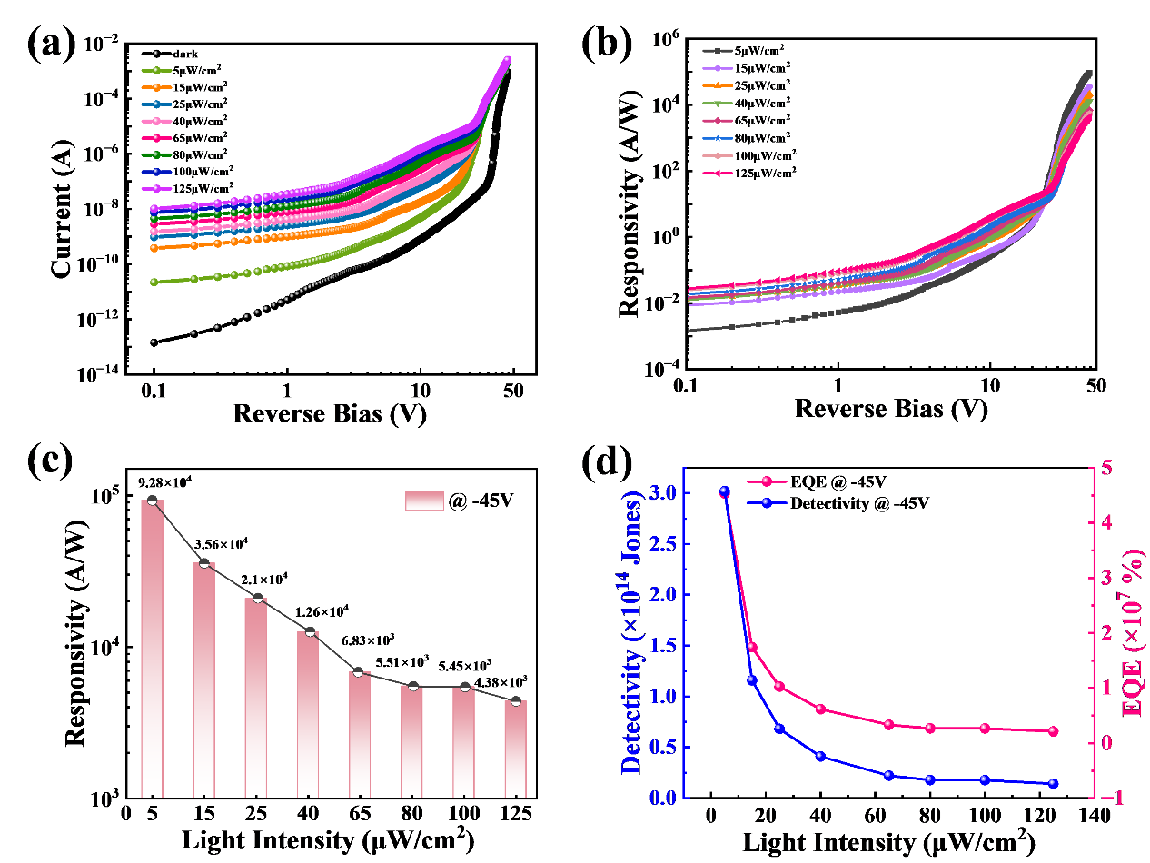
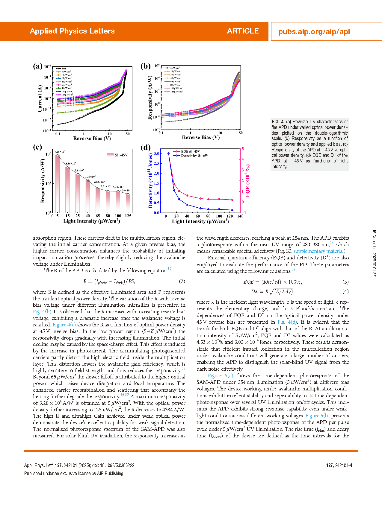
FIG. 4. (a) Reverse I–V characteristics of the APD under varied optical power densities plotted on the double-logarithmic scale. (b) Responsivity as a function of optical power density and applied bias. (c) Responsivity of the APD at -45 V vs optical power density. (d) EQE and D* of the APD at -45 V as functions of light intensity.
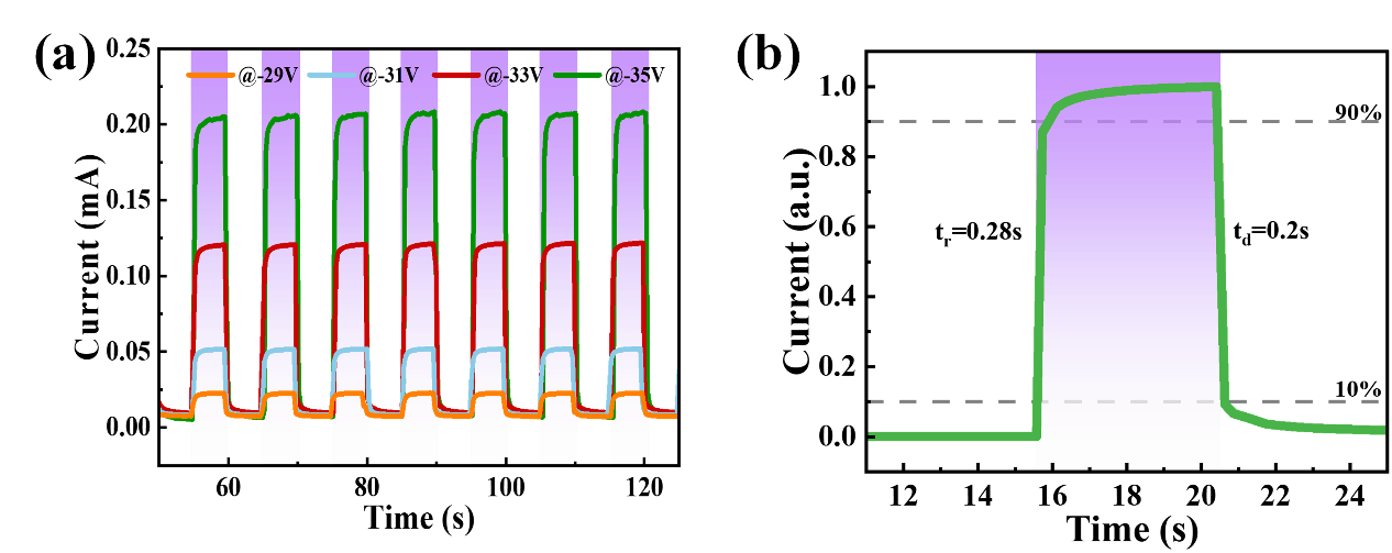
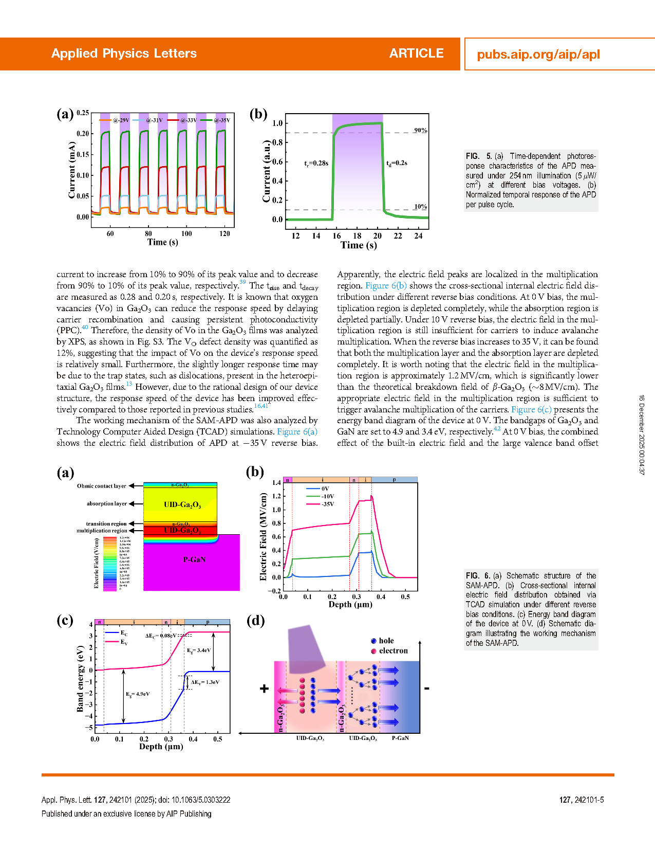
FIG. 5. (a) Time-dependent photoresponse characteristics of the APD measured under 254 nm illumination (5 μW/cm2) at different bias voltages. (b) Normalized temporal response of the APD per pulse cycle.
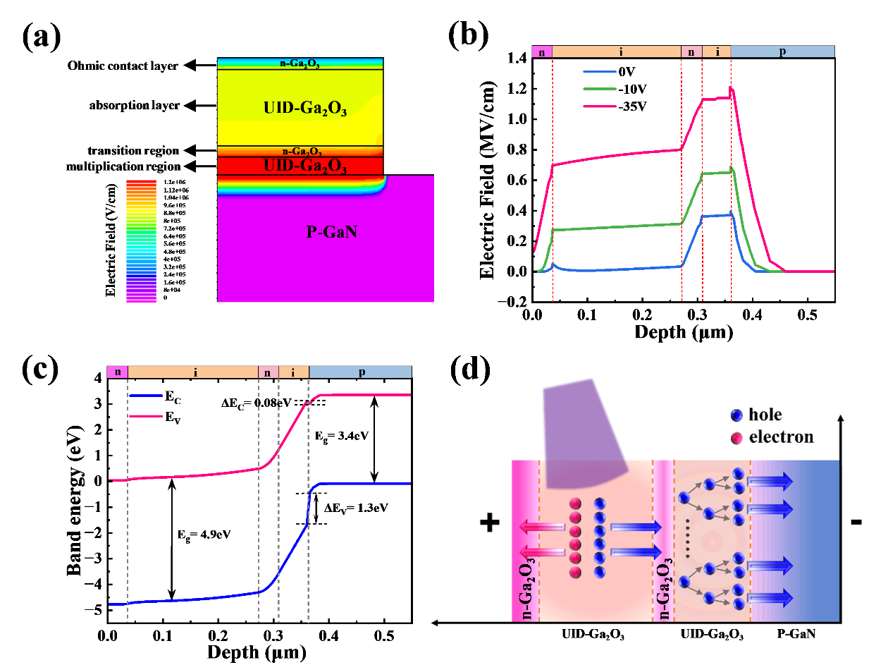
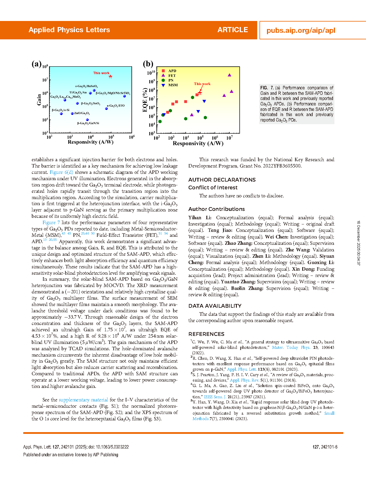
FIG. 6. (a) Schematic structure of the SAM-APD. (b) Cross-sectional internal electric field distribution obtained via TCAD simulation under different reverse bias conditions. (c) Energy band diagram of the device at 0 V. (d) Schematic diagram illustrating the working mechanism of the SAM-APD.
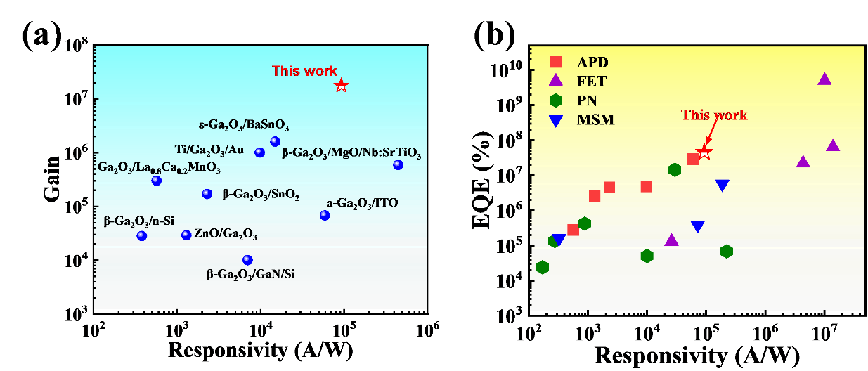
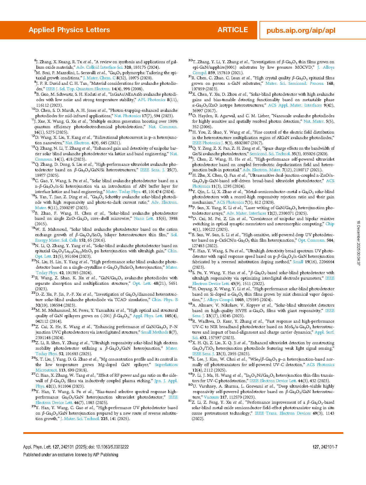
FIG. 7. (a) Performance comparison of Gain and R between the SAM-APD fabricated in this work and previously reported Ga2O3 APDs. (b) Performance comparison of EQE and R between the SAM-APD fabricated in this work and previously reported Ga2O3 PDs.
DOI:
doi.org/10.1063/5.0303222