Paper Sharing
【Member Papers】Ultralow On-Resistance High-Voltage β-Ga₂O₃ MOSFET With an Extended p-NiO Gate Field Plate
日期:2025-12-23阅读:535
Researchers from the University of Electronic Science and Technology of China have published a dissertation titled "Ultralow On-Resistance High-Voltage β-Ga2O3 MOSFET With an Extended p-NiO Gate Field Plate" in IEEE Transactions on Electron Devices.
Project Support
This work was supported in part by the National Natural Science Foundation of China under Grant 62374028 and Grant 62404030, in part by the Postdoctoral Fellowship Program of China Postdoctoral Science Foundation (CPSF) under Grant GZC20240199 and Grant GZC20240200, and in part by the Central Government-Guided Local-Free Exploration Project under Grant 2023ZYD0160.
Background
Ultrawide bandgap semiconductor β-Ga2O3 has exhibited extraordinary potential for next-generation power devices, owing to ultrawide bandgap of 4.5–4.9 eV, high critical electric field (E-field) ∼ 8 MV/cm, high Baliga’s figure-of-merit (BFOM = εsµnE3c) and cost-effective growing methods. Over the past decade, β-Ga2O3 MOSFETs have attracted a great deal of attention due to the great advantages in power applications. Enormous efforts have been made to improve their power figure of merit (PFOM = breakdown voltage (BV)2 /Ron,sp) by extreme-κ dielectrics, FinFET, superjunction, RESURF among others. Moreover, low-negative threshold voltage (Vth) value is required to reduce static power consumption and enhance circuit security in power conversion application. Gate recess heterojunction gate, current block layer (CBL) are effective solutions to improve the Vth. However, it is challenging to improve both Ron,sp and BV simultaneously because the high drift concentration for low Ron,sp easily leads to premature breakdown. In this work, we demonstrated and investigated a novel β-Ga2O3 MOSFET with an extended p-NiO gate field plate (PFP MOSFET) by Sentaurus TCAD. Different from common RESURF devices reducing the Ron,sp by assisted depletion effect to increase the Nd, the proposed device introduces the accumulation layer to further decrease the Ron,sp; therefore, the proposed PFP MOSFET can achieve a better trade-off between BV and Ron,sp.
Abstract
A novel β-Ga2O3 MOSFET with an extended p-NiO gate field plate (PFP) is proposed and investigated. The extended p-NiO gate is separated from the Ga2O3 N-drift by Al2O3 dielectric layer and forms a metal/insulator/semiconductor (MIS) with Al2O3/Ga2O3 N-drift. In the on-state, a high-density electron layer is accumulated along the N-drift surface to provide an additional ultralow-resistance current path, and thus dramatically reduces specific on-resistance (Ron,sp). In the off-state, the PFP improves breakdown voltage (BV) by modulating the E -field distribution and assisting to deplete N-drift. Therefore, PFP MOSFET allows a higher N-drift doping concentration (Nd) to reduce Ron,sp without significant BV degradation. Compared with the MOSFET without PFP, the proposed device decreases the Ron,sp by 45% and increases the BV by 407%, resulting in a high PFOM up to 1.63 GW/cm2. This work provides a new insight into realizing a high-performance β-Ga2O3 MOSFET for future power conversion applications.
Conclusion
An ultralow Ron,sp and high BV β-Ga2O3 MOSFET is proposed and investigated. The proposed MOSFET features an extended p-NiO gate field plate (PFP). The PFP induces an electron accumulation layer in the ON-state to achieve an ultralow Ron,sp and modulates E-field distribution to enhance BV in the OFF-state. By optimizing key parameters, PFP MOSFET exhibit Ron,sp of 6.4 mΩ · cm2 and BV of 3230 V, resulting in a high PFOM up to 1.63 GW/cm2. Compared with PG MOSFET, the Ron,sp and BV of the PFP MOSFET are improved by 45% and 407%, respectively; therefore, the PFP MOSFET achieves better trade-off between Ron,sp and BV, exhibiting extraordinary figure of merit.
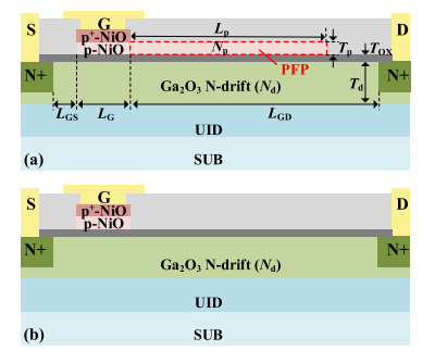
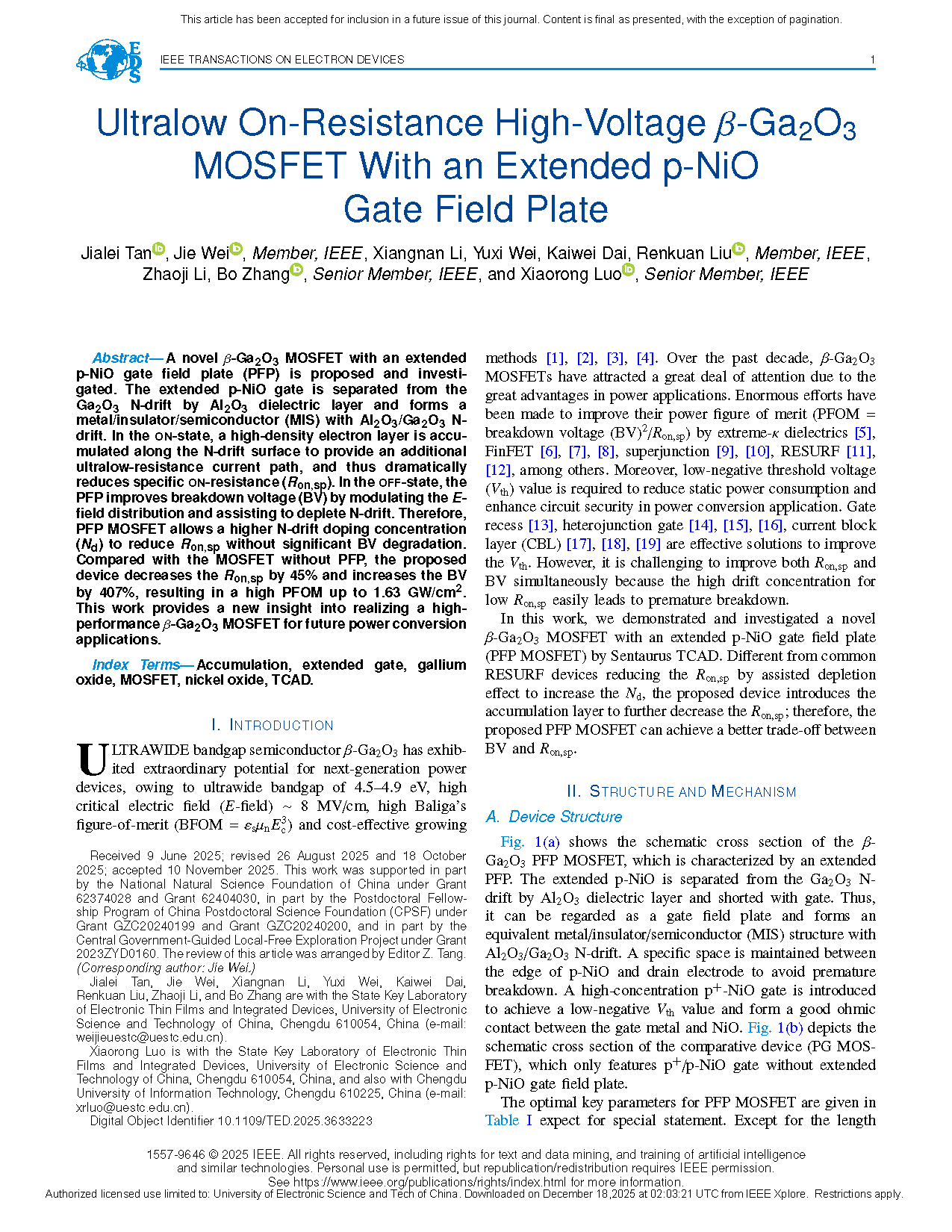
Fig. 1. Schematic cross section of (a) PFP MOSFET and (b) PG MOSFET.
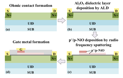
Fig. 2. Key fabrication process for PFP MOSFET. (a) Source-drain ohmic contact formation. (b) Form the Al2O3 dielectric layer by atomic layer deposition. (c) Deposit double-layered NiO by the RF sputtering. (d) Form the gate metal.
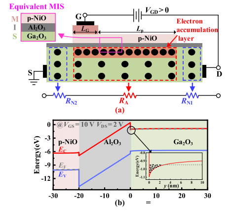
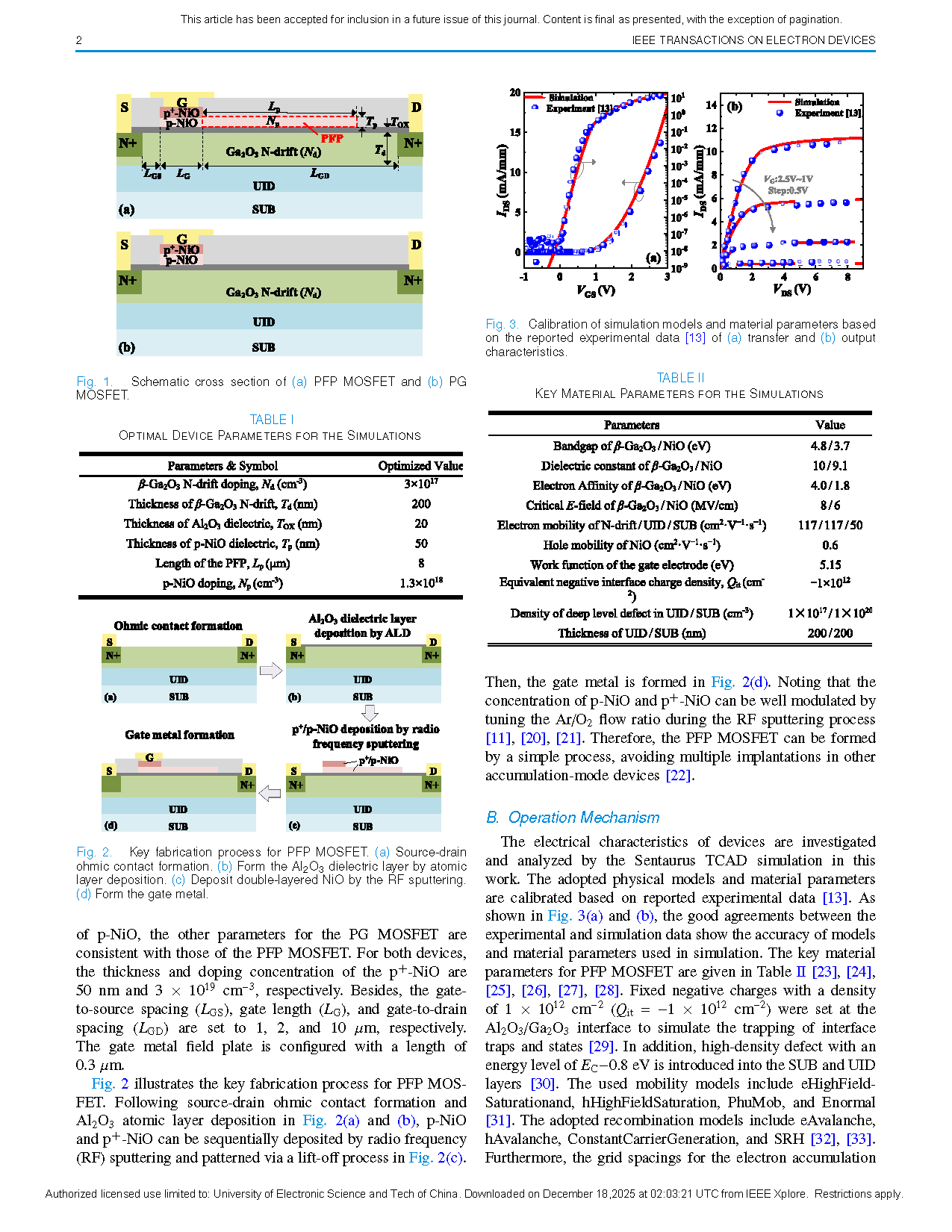
Fig. 3. (a) Operating mechanism and (b) NiO/Al2O3/Ga2O3 energy band distribution of PFP MOSFET in the ON-state.
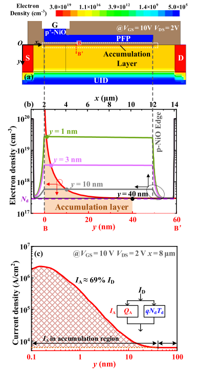
Fig. 4. Electron density (a) contours and (b) distribution in the x- and y-dimensions of PFP MOSFET at VGS = 10 V and VDS = 2 V. (c) Current density distribution in the y-dimension of PFP MOSFET at VGS = 10 V, VDS = 2 V and x = 8 µm.
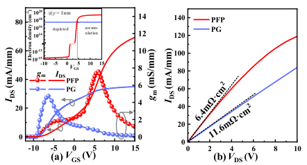
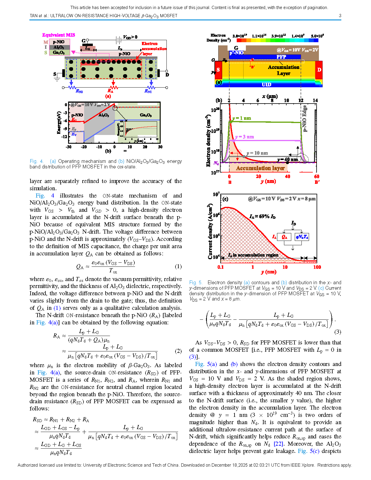
Fig. 5. (a) Transfer characteristics for PFP and PG MOSFET @ VDS = 4 V. The inset shows the electron density of the two devices @ y = 1 nm as a function of VGS. (b) Output characteristics for different MOSFETs @ VGS = 10 V.
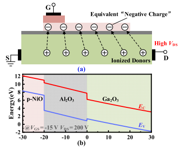
Fig. 6. (a) Operating mechanism and (b) NiO/Al2O3/Ga2O3 energy band distribution of PFP MOSFET in the OFF-state.
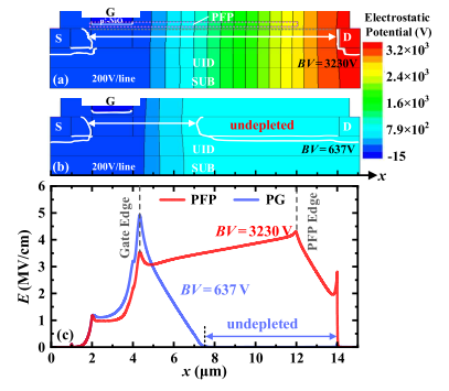
Fig. 7. Potential and depletion region contours of (a) PFP MOSFET and (b) PG MOSFET at breakdown. (c) E-field (E) along Ga2O3 N-drift surface of PFP and PG MOSFET at breakdown.
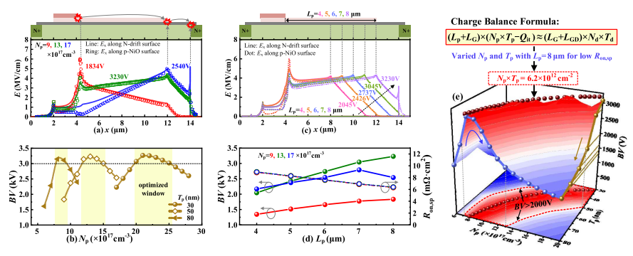
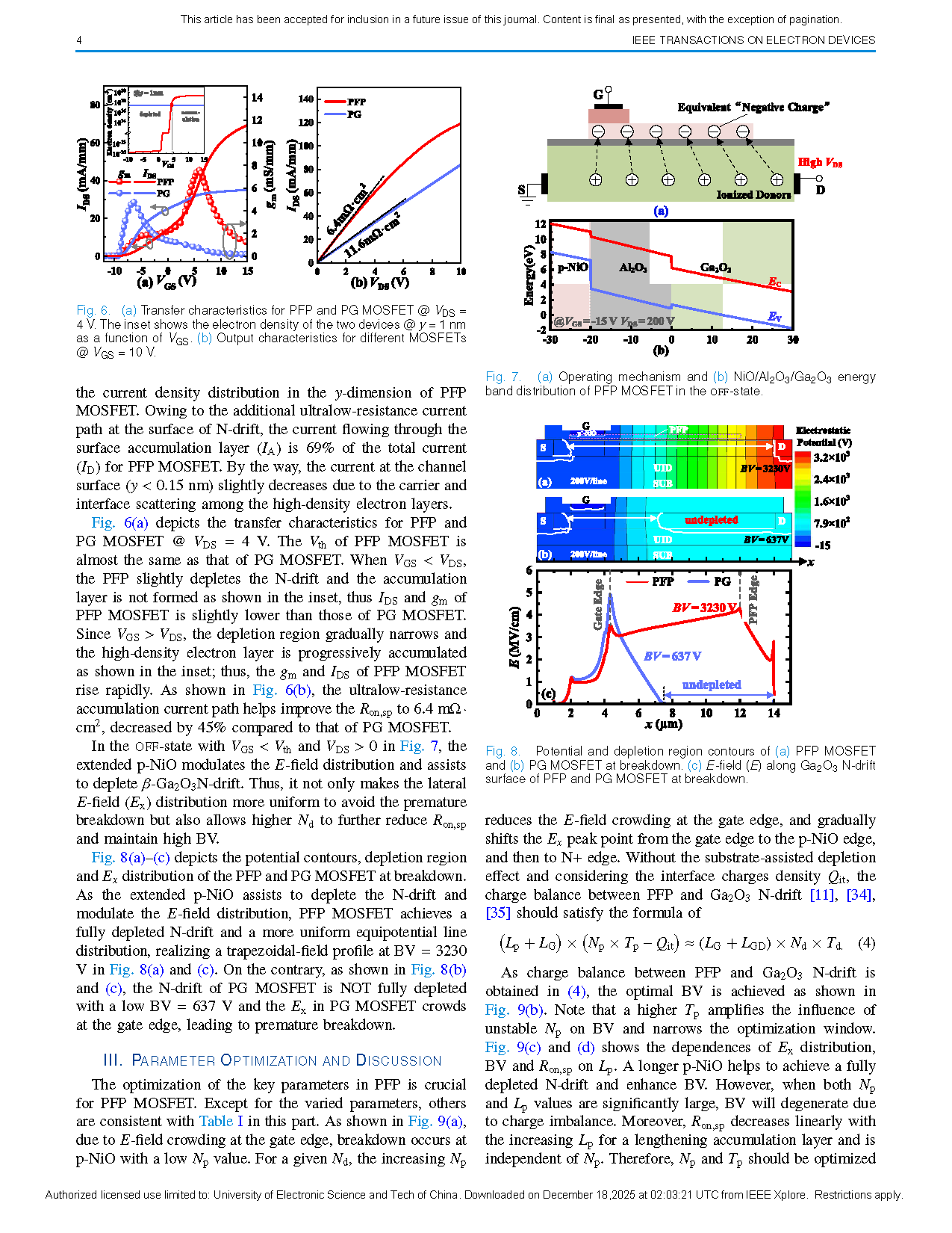
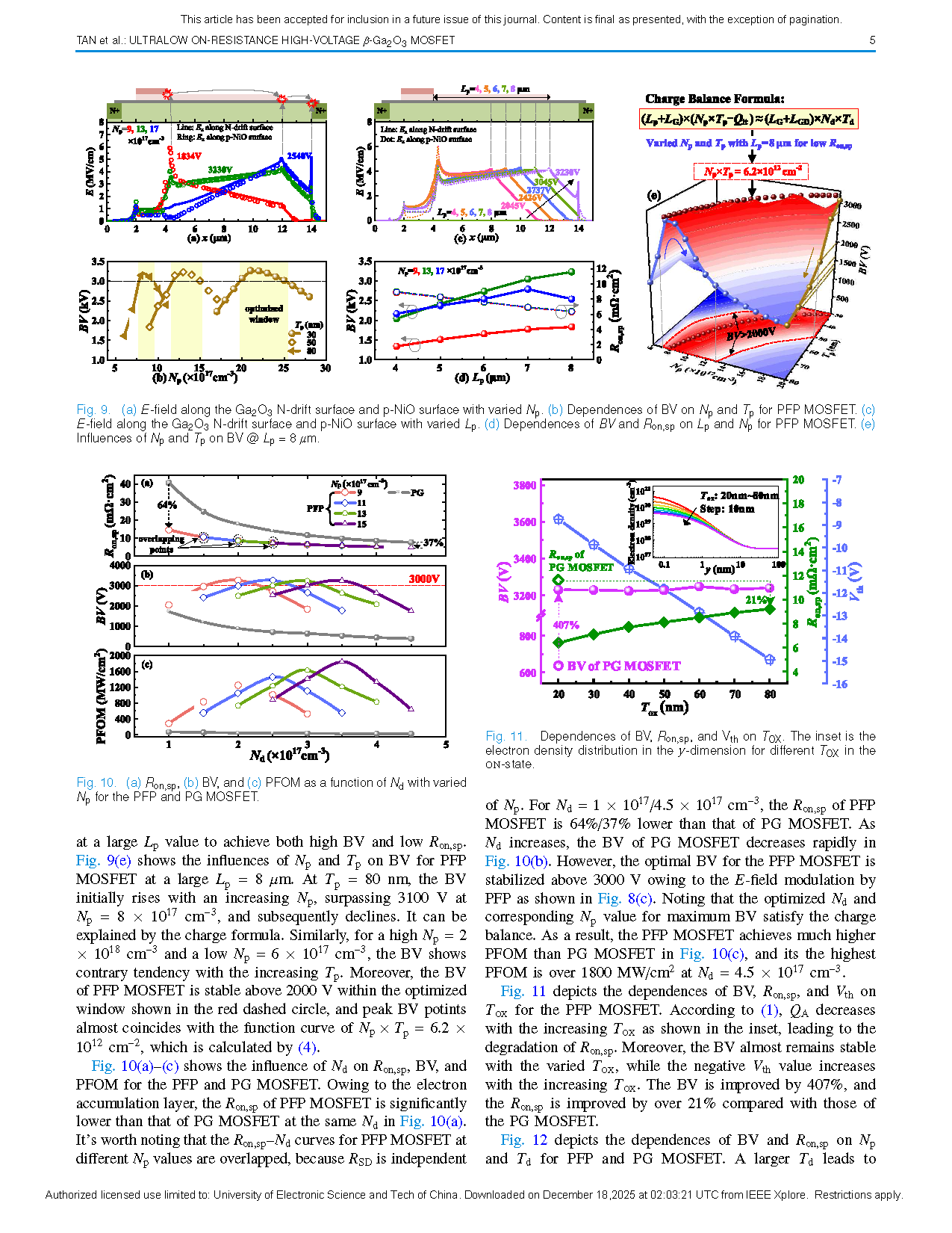
Fig. 8. (a) E-field along the Ga2O3 N-drift surface and p-NiO surface with varied Np. (b) Dependences of BV on Np and Tp for PFP MOSFET. (c) E-field along the Ga2O3 N-drift surface and p-NiO surface with varied Lp. (d) Dependences of BV and Ron,sp on Lp and Np for PFP MOSFET. (e) Influences of Np and Tp on BV @ Lp = 8 µm.
DOI:
doi.org/10.1109/TED.2025.3633223