Paper Sharing
【Member Papers】Multi-modal thermography-calibrated barrier in vertical β-Ga₂O₃ Schottky barrier diodes
日期:2025-12-23阅读:492
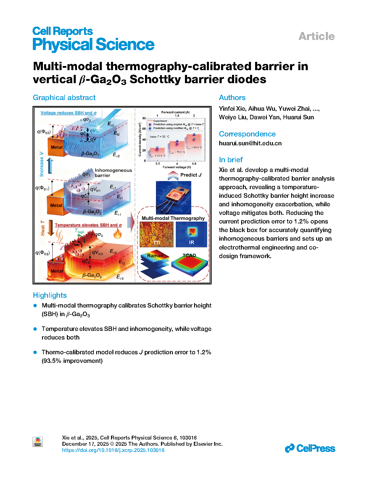
Researchers from the Harbin Institute of Technology, Shenzhen have published a dissertation titled "Multi-modal thermography-calibrated barrier in vertical β-Ga2O3 Schottky barrier diodes" in Cell Reports Physical Science. Dr. Yinfei Xie is the first author, and Prof. Huarui Sun is the corresponding author of the study.
Background
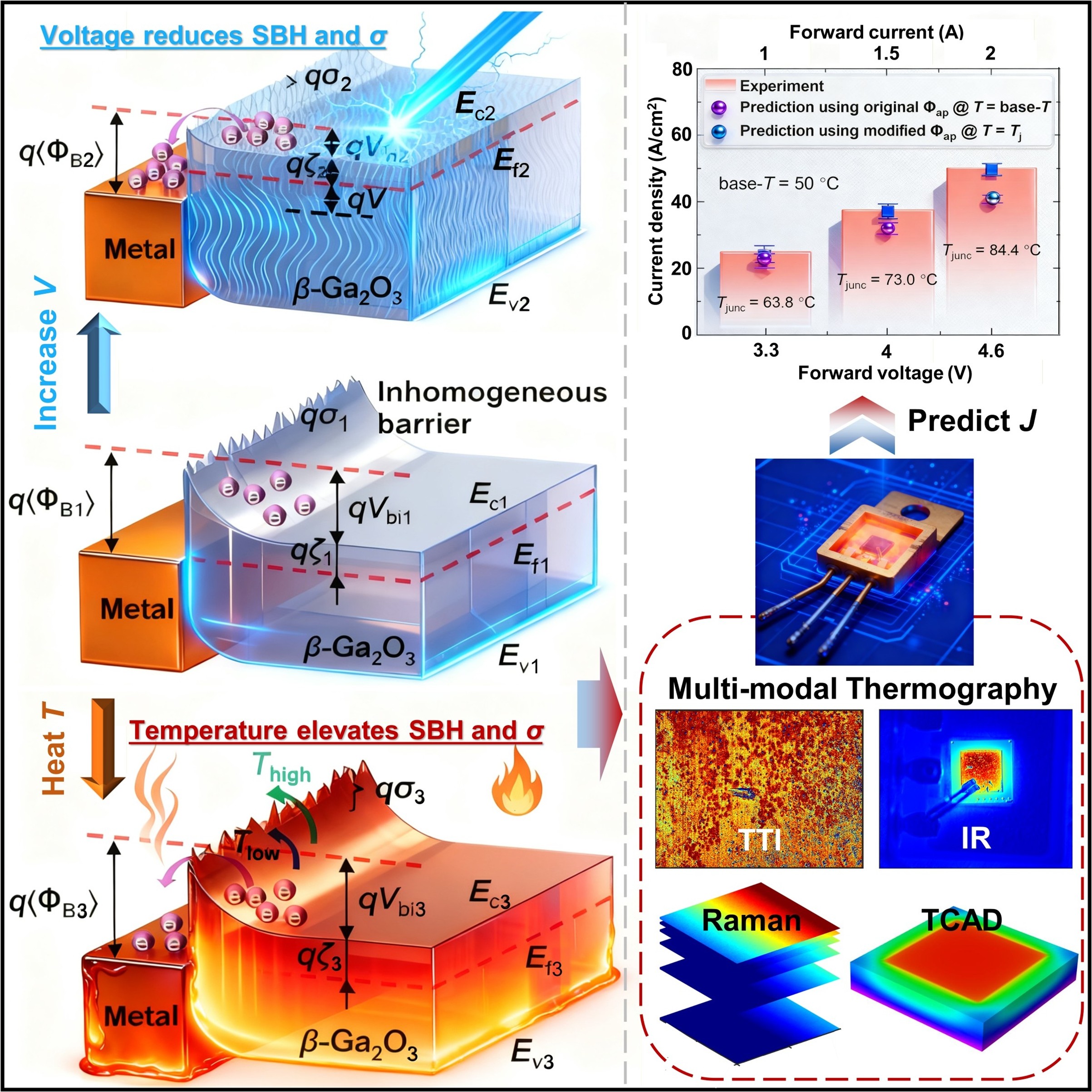
β-Ga2O3 has emerged as a promising material for next-generation high-power electronics due to its ultrahigh critical electric field (8 MV/cm), superior Baliga’s figure of merit (BFOM = 3444, compared to silicon), and compatibility with low-cost crystal growth. Vertical β-Ga2O3 Schottky barrier diodes (SBDs) are attractive for high-voltage, high-temperature, and energy-efficient power conversion systems. However, fully leveraging β-Ga2O3 requires addressing fundamental challenges in Schottky barrier engineering, particularly the voltage- and temperature-dependent Schottky barrier height (SBH) and its spatial inhomogeneity (σ), which critically affect current transport and device reliability. Although recent work has improved thermal management (e.g., nanoporous substrates, heterostructures) and electrical performance (e.g., surface passivation, doping), the microscopic mechanisms governing current transport in devices with inhomogeneous SBHs remain unclear. Conventional SBH characterization methods, often limited to single-temperature or low-frequency measurements, neglect coupled voltage-temperature effects. Barrier inhomogeneities caused by defects, interface roughness, or compositional variations can lead to current crowding, localized heating, and premature device failure. Additionally, standard techniques such as static I–V measurements or single-modality thermography lack the temporal and spatial resolution to capture voltage- and temperature-dependent transients and nanoscale temperature gradients, limiting understanding of dynamic SBH evolution under operational stresses.
Main content
Xie et al. developed a closed-loop electro-thermal barrier co-analysis framework by integrating high-resolution 3D Raman thermography, infrared, thermoreflectance, temperature-dependent electrical measurements (J–V–T/C–V–T), and physics-based modeling. The study reveals that rising temperature increases both the average Schottky barrier height (SBH) and its spatial nonuniformity (σ), while applied bias suppresses fluctuations via a homogenizing effect. This dynamic electro-thermal feedback governs the non-monotonic I–V characteristics of β-Ga2O3 Schottky diodes under high-power operation. Critically, the experimentally calibrated model was embedded into TCAD, enabling highly accurate J–V prediction. Traditional models ignoring Joule heating underestimate SBH by up to 10.6%. With thermal compensation, both SBH and σ increase, aligning with simulations. Incorporating real-time electro-thermal feedback reduces current density prediction error from 18.4% to just 1.2%. This work demystifies the "barrier ambiguity" in β-Ga2O3 Schottky interfaces and establishes a general, mechanism-driven electro-thermal co-design methodology, marking a shift from empirical fitting to physics-aware modeling, accelerating the industrial adoption of wide-bandgap semiconductor devices.
Highlight
● Multi-modal thermography calibrates Schottky barrier height (SBH) in β-Ga2O3
● Temperature elevates SBH and inhomogeneity, while voltage reduces both
● Thermo-calibrated model reduces Jprediction error to 1.2% (93.5% improvement)
Conclusion
The multimodal thermography-based calibration framework reveals that temperature elevation increases both the Schottky barrier height and its spatial inhomogeneity, whereas applied voltage mitigates these effects. The revised barrier model significantly enhances the accuracy of current density prediction, offering new insights for precisely quantifying barrier inhomogeneity and rationally engineering Schottky contacts. This work lays a critical foundation for improving the reliability of β-Ga2O3 SBDs in high-power applications.
Graphical Abstract
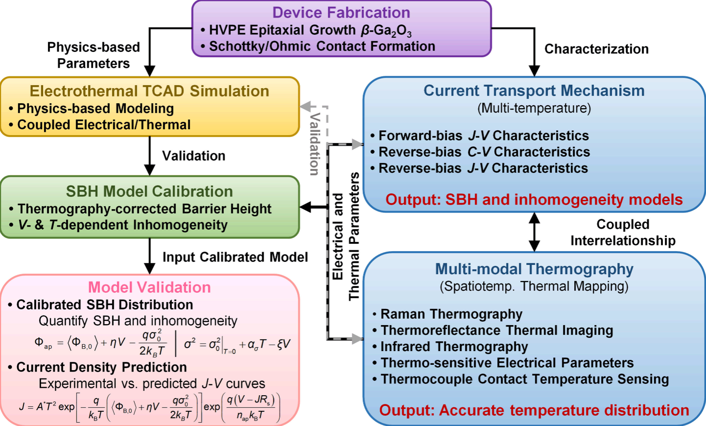
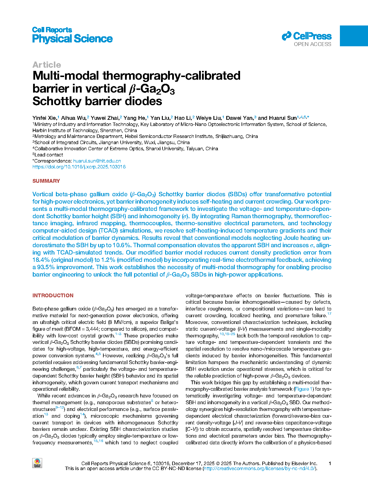
Figure 1 Framework for multi-modal thermography-calibrated barrier analysis

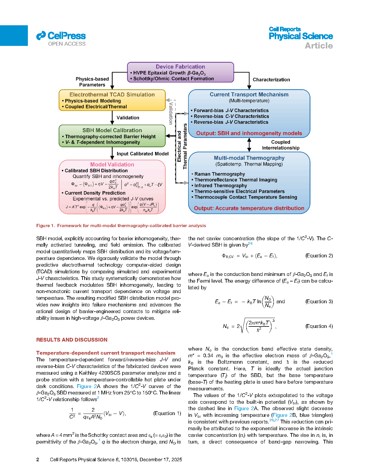
Figure 2 Reverse-bias C-V characteristics. (A) 1/C2-V characteristics of the fabricated vertical β-Ga2O3 SBD measured at the temperature range of 25 °C–150 °C. (B) Dependence of the built-in potential (qVbi), Schottky barrier height (qΦB,CV), and net donor concentration (ND) extracted from C-V-T characteristics as a function of T.

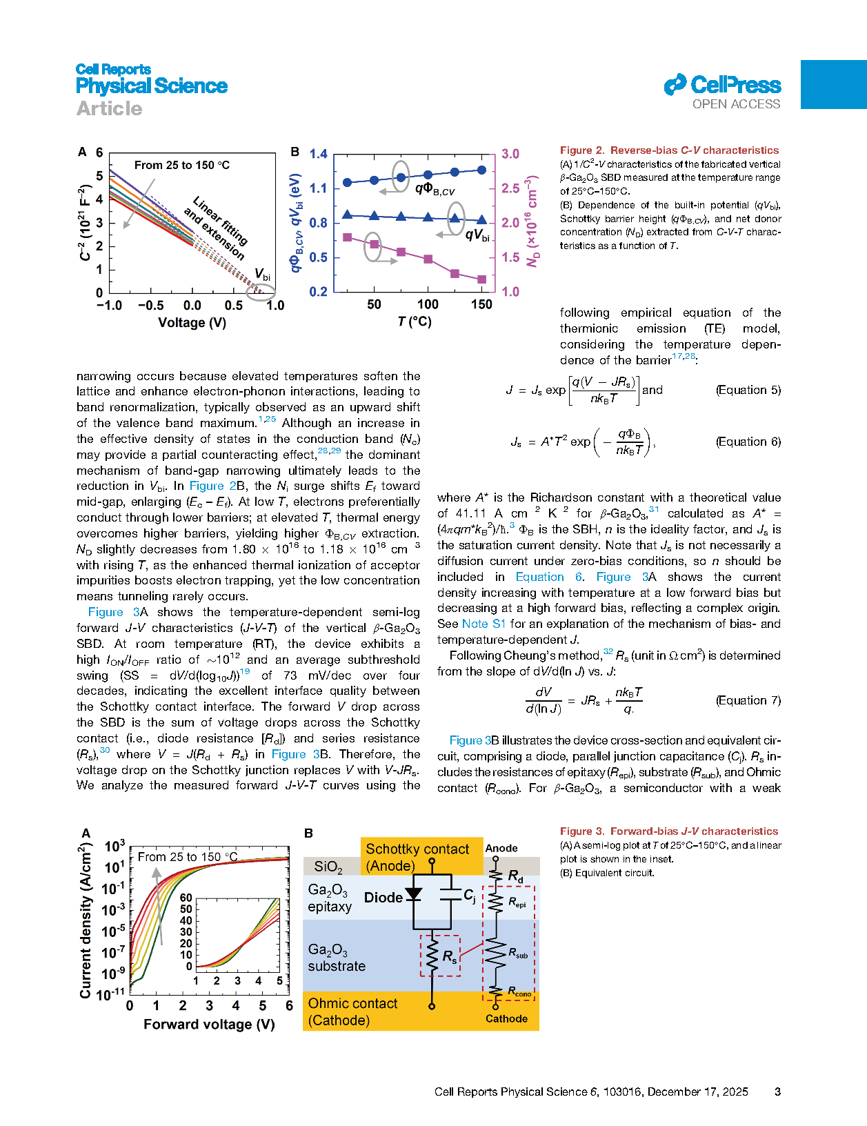
Figure 3 Forward-bias J-V characteristics. (A) A semi-log plot at T of 25°C–150°C, and a linear plot is shown in the inset. (B) Equivalent circuit.

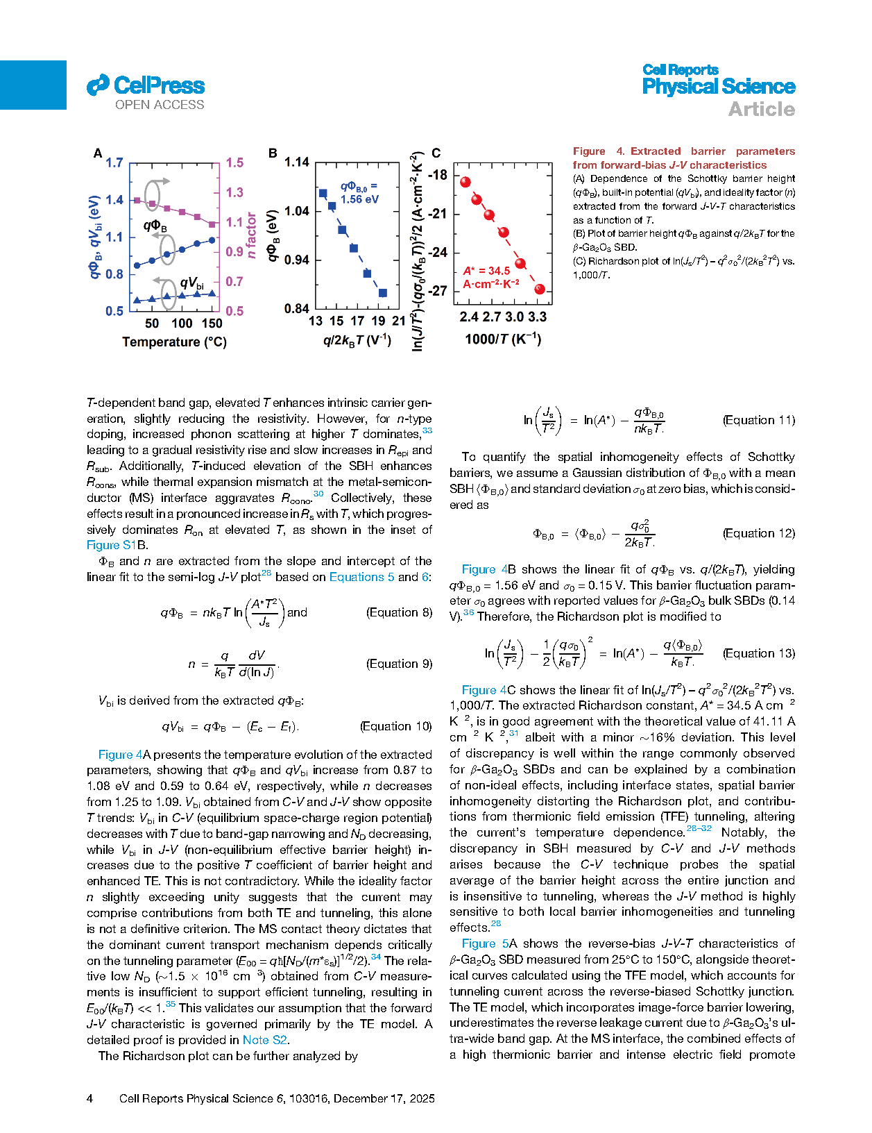
Figure 4 Extracted barrier parameters from forward-bias J-V characteristics (A) Dependence of the Schottky barrier height (qΦB), built-in potential (qVbi), and ideality factor (n) extracted from the forward J-V-T characteristics as a function of T. (B) Plot of barrier height qΦB against q/2kBT for the β-Ga2O3 SBD. (C) Richardson plot of ln(Js/T2) – q2σ02/(2kB2T2) vs. 1,000/T.
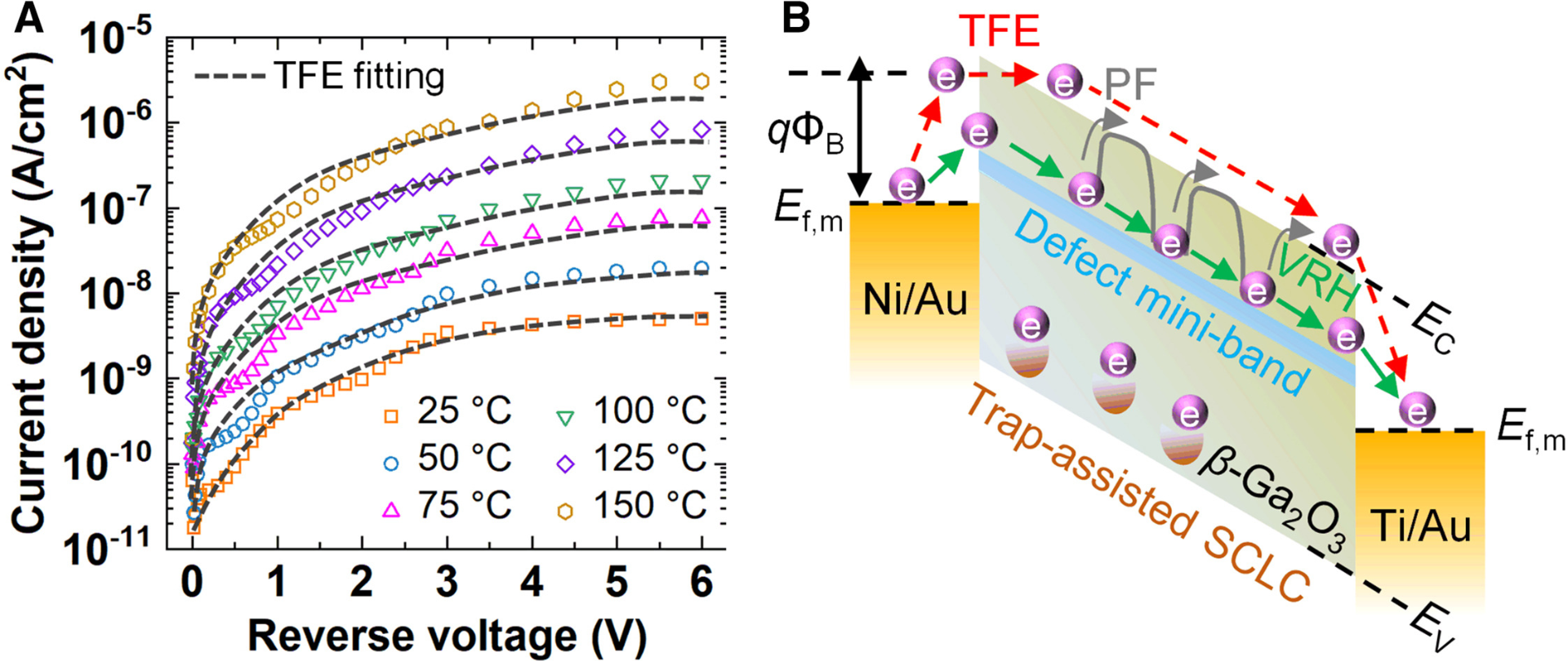
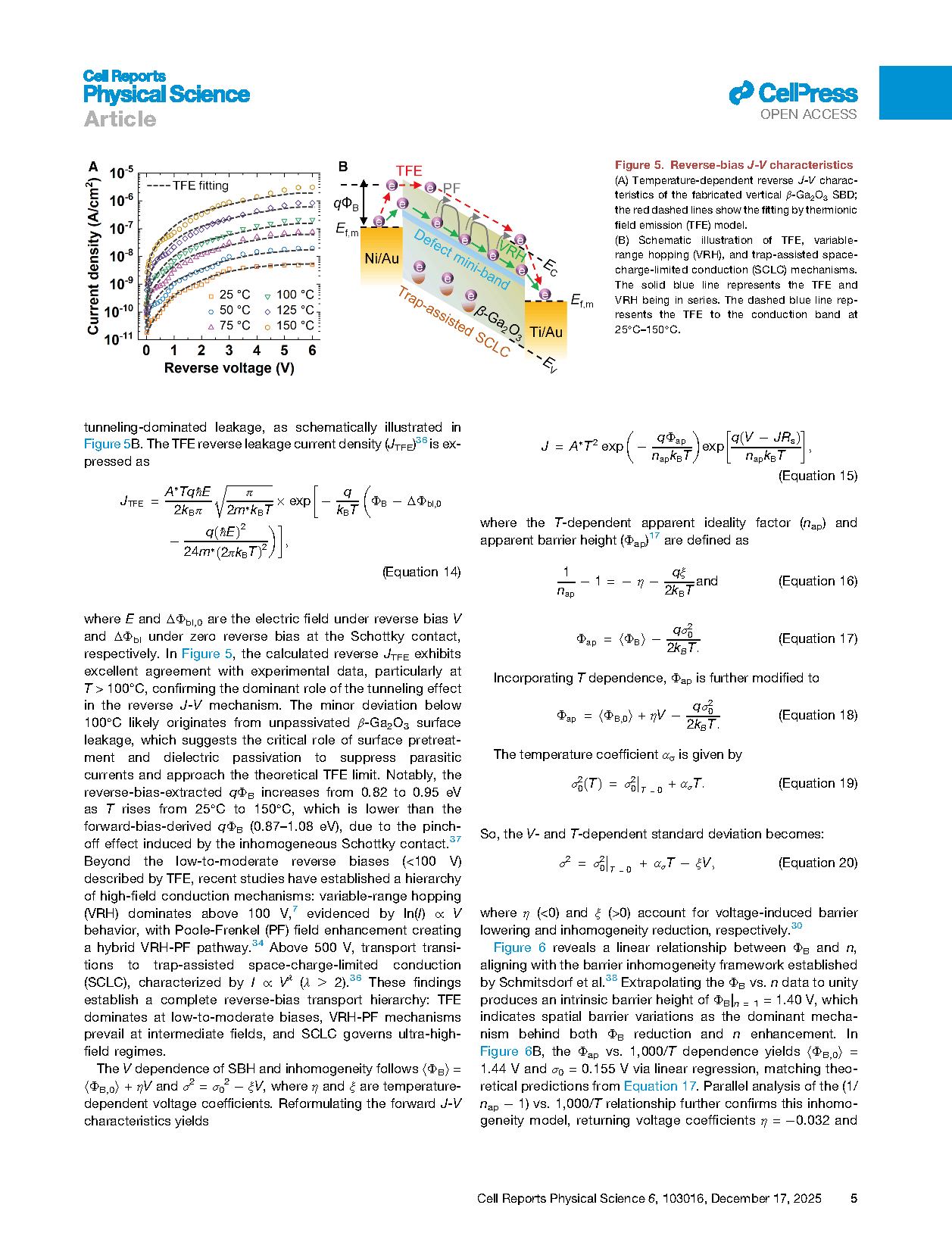
Figure 5 Reverse-bias J-V characteristics. (A) Temperature-dependent reverse J-V characteristics of the fabricated vertical β-Ga2O3 SBD; the red dashed lines show the fitting by thermionic field emission (TFE) model. (B) Schematic illustration of TFE, variable-range hopping (VRH), and trap-assisted space-charge-limited conduction (SCLC) mechanisms. The solid blue line represents the TFE and VRH being in series. The dashed blue line represents the TFE to the conduction band at 25°C–150°C.
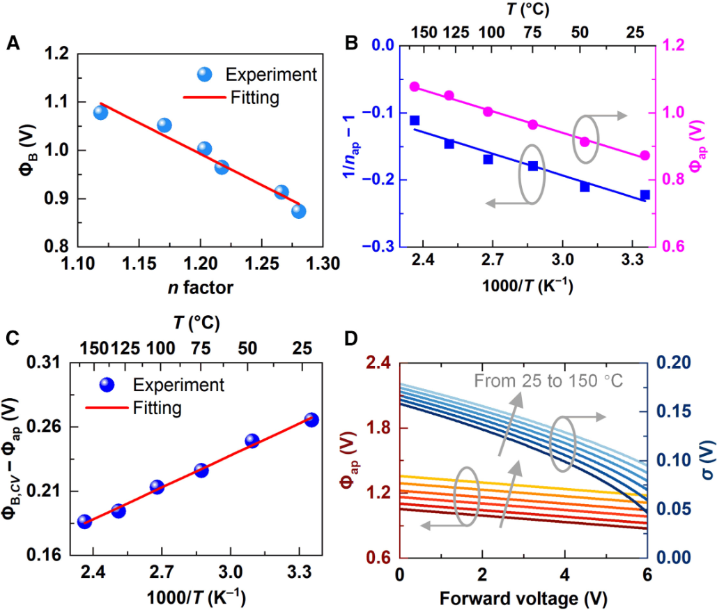
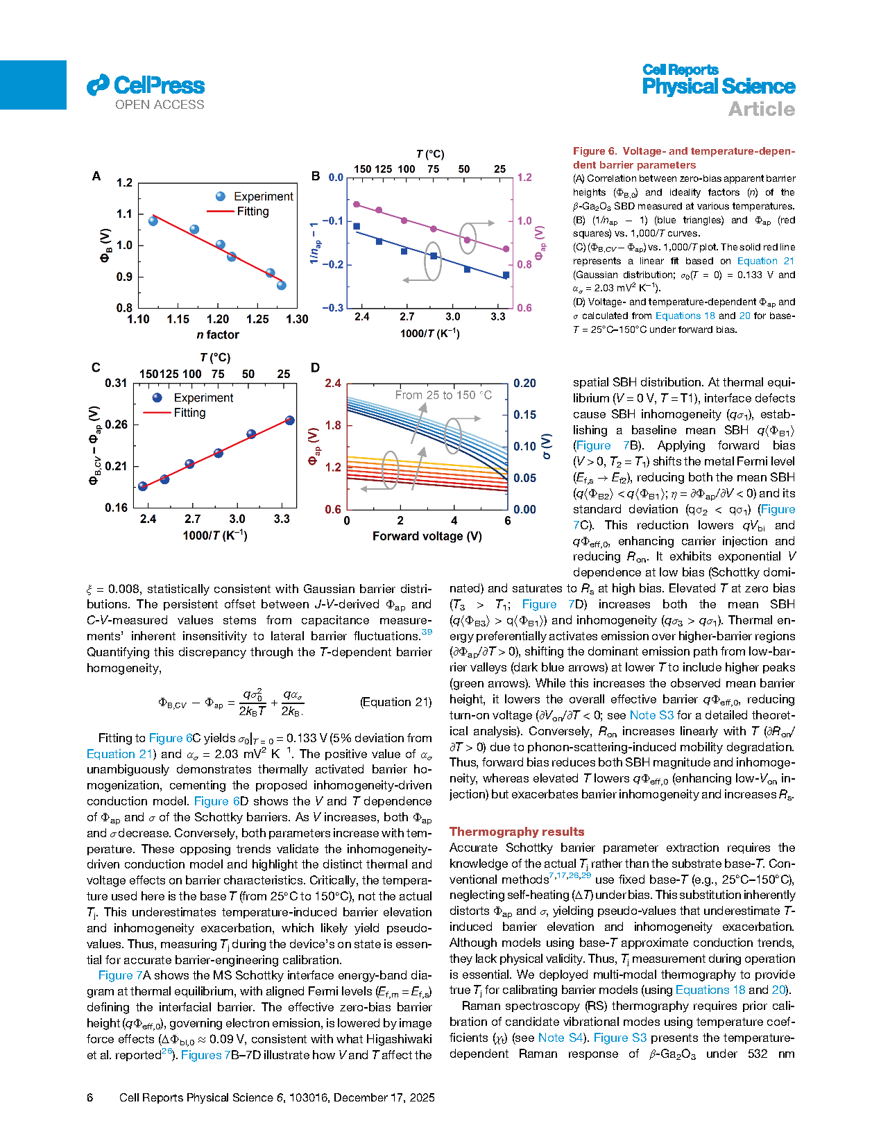
Figure 6 Voltage- and temperature-dependent barrier parameters. (A) Correlation between zero-bias apparent barrier heights (ΦB,0) and ideality factors (n) of the β-Ga2O3 SBD measured at various temperatures. (B) (1/nap − 1) (blue triangles) and Φap (red squares) vs. 1,000/T curves. (C) (ΦB,CV − Φap) vs. 1,000/T plot.
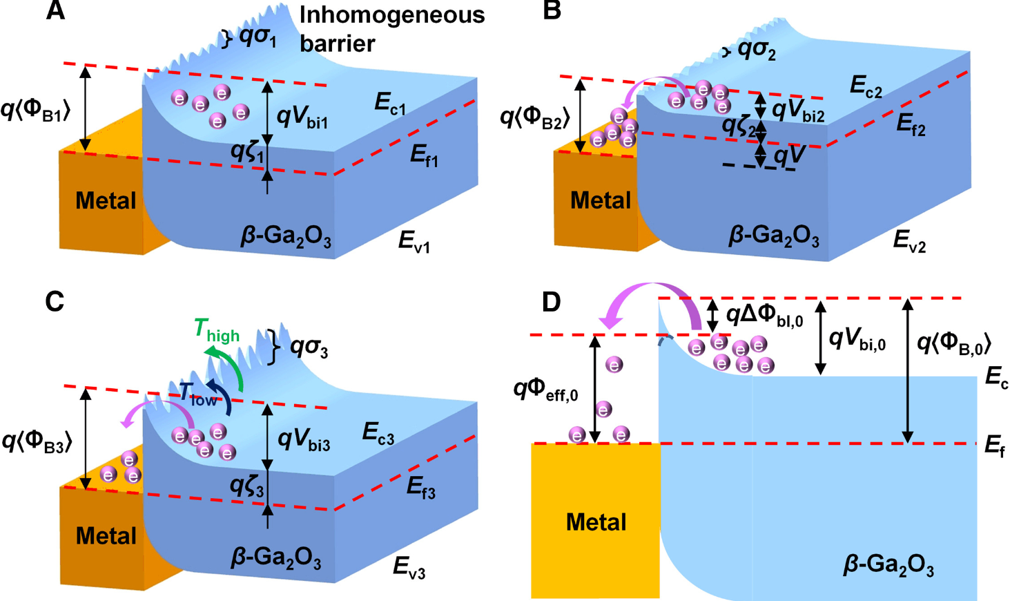
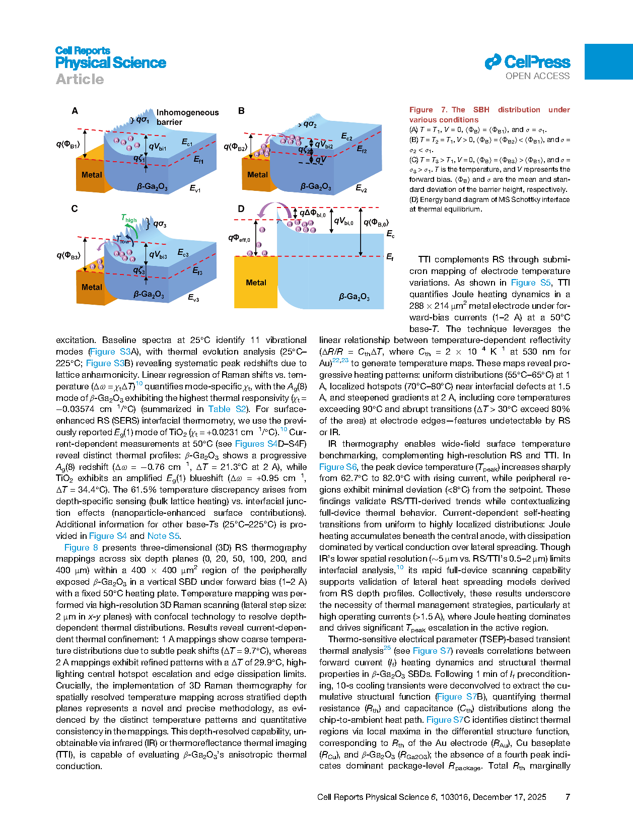
Figure 7 The SBH distribution under various conditions. (A) T = T1, V = 0, ⟨ΦB⟩ = ⟨ΦB1⟩, and σ = σ1. (B) T = T2 = T1, V > 0, ⟨ΦB⟩ = ⟨ΦB2⟩ < ⟨ΦB1⟩, and σ = σ2 < σ1. (C) T = T3 > T1, V = 0, ⟨ΦB⟩ = ⟨ΦB3⟩ > ⟨ΦB1⟩, and σ = σ3 > σ1. T is the temperature, and V represents the forward bias. ⟨ΦB⟩ and σ are the mean and standard deviation of the barrier height, respectively. (D) Energy band diagram of MS Schottky interface at thermal equilibrium.

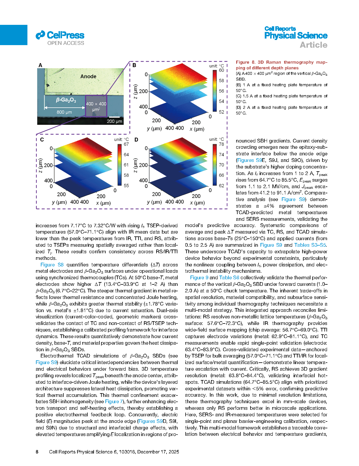
Figure 8 3D Raman thermography mapping of different depth planes. (A) A 400 × 400 μm2 region of the vertical β-Ga2O3 SBD. (B) 1 A at a fixed heating plate temperature of 50 °C. (C) 1.5 A at a fixed heating plate temperature of 50°C. (D) 2 A at a fixed heating plate temperature of 50°C.
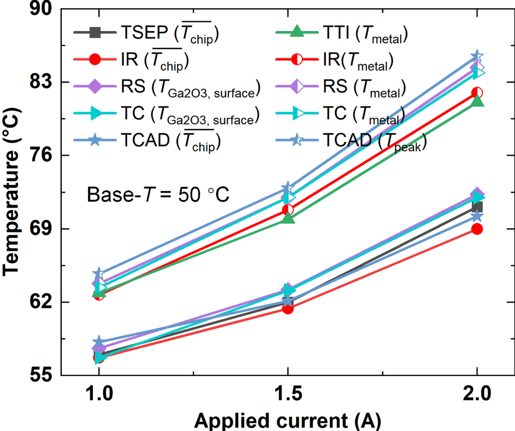
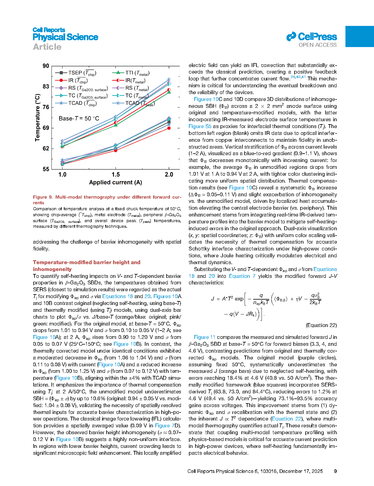
Figure 9 Multi-modal thermography under different forward currents. Comparison of temperature analysis at a fixed chuck temperature of 50 °C, showing chip-average (¯Tchip), metal electrode (Tmetal), peripheral β-Ga2O3 surface (TGa2O3, surface), and overall device peak (Tpeak) temperatures, measured by different thermography techniques.

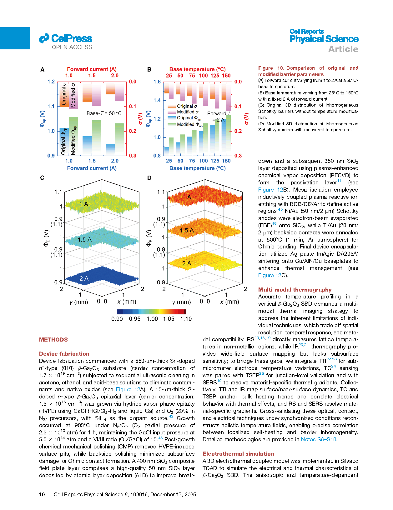
Figure 10 Comparison of original and modified barrier parameters. (A) Forward current varying from 1 to 2 A at a 50 °C-base temperature. (B) Base temperature varying from 25 °C to 150 °C with a fixed 2 A of forward current. (C) Original 3D distribution of inhomogeneous Schottky barriers without temperature modification. (D) Modified 3D distribution of inhomogeneous Schottky barriers with measured temperature.
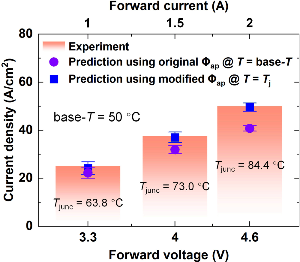
Figure 11 Prediction of forward-bias current density before and after temperature compensation. Comparison of experimentally measured current density with calculated values based on the original and modified Φap under different forward-bias conditions at a base temperature of 50°C. Error bars indicate uncertainties in the current prediction arising from barrier inhomogeneity.
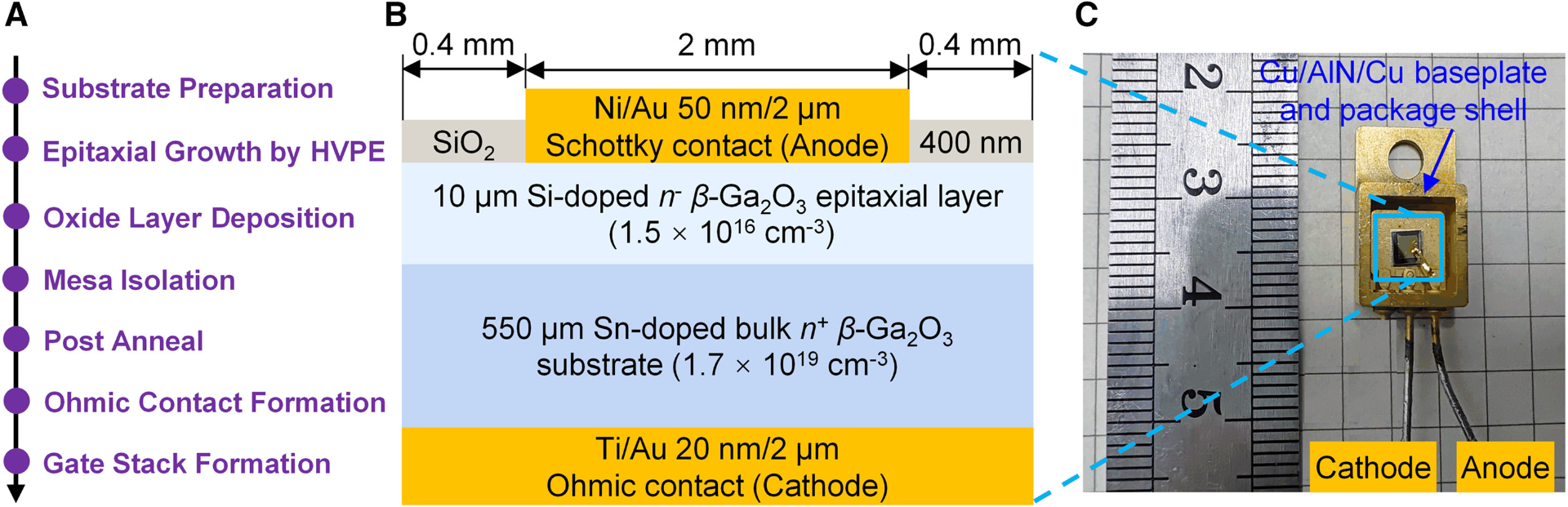
Figure 12 Fabrication of vertical β-Ga2O3 SBD. (A) Illustration of the main steps for device fabrication. (B) Schematic cross-sectional structure. (C) Optical image of whole packaged device.

Huarui Sun is a Professor, Doctoral Supervisor, and Associate Dean of the School of Science at Harbin Institute of Technology, Shenzhen. His research focuses on characterization of semiconductor materials and devices, with recent work advancing thermal analysis methods for wide-bandgap semiconductors, revealing the origins of thermal resistance, and establishing electro-thermal co-design strategies. He also clarified the physical origin and modulation mechanisms of Raman anisotropy in two-dimensional semiconductors.
He has published over 70 papers in high-impact journals such as Physical Review Letters, Laser & Photonics Reviews, and Nature-family journals, holds more than ten invention patents, and was awarded the Guangdong Provincial Young Top-notch Talent in Science and Technology Innovation. He serves as a Young Editorial Board Member of Journal of Synthetic Crystals and an Executive Committee Member of the Surface Analysis Division of the Guangdong Association of Analytical Testing.

Yinfei Xie is a Ph.D. candidate in Physics at Harbin Institute of Technology, Shenzhen, specializing in thermal reliability and electro-thermal co-optimization of ultra-wide bandgap semiconductor devices. He published over 10 SCI papers in prestigious international journals and conferences, including Cell Reports Physical Science, Nano Letters, Nano Research, ACS Applied Materials & Interfaces, Applied Physics Letters, IEEE Transactions on Electron Devices, and IEEE EDTM.
Dr. Xie holds ten Chinese national patents (filed or granted). He has received several honors and awards, such as the inaugural China Association for Science and Technology (CAST) Young Talent Support (Doctoral Candidate), National Scholarship for Doctoral Students, Outstanding Scientific and Technological Talent of Heilongjiang Provincial Association for Science and Technology, and Outstanding Graduate Student of Heilongjiang Province.
Yinfei Xie, Aihua Wu, Yuwei Zhai, Yang He, Yan Liu, Hao Li, Weiye Liu, Dawei Yan, and Huarui Sun. Multi-modal Thermography-Calibrated Barrier in Vertical β-Ga2O3 Schottky Barrier Diodes. Cell Reports Physical Science, 2025, 6(12): 103016.
DOI:https://doi.org/10.1016/j.xcrp.2025.103016