Paper Sharing
【Domestic Papers】High-performance solar-blind optoelectronic synaptic device based on N-doped Ga₂O₃ nanowire network for neuromorphic computing
日期:2025-12-24阅读:472
Researchers from the Zhejiang Sci-Tech University have published a dissertation titled "High-performance solar-blind optoelectronic synaptic device based on N-doped Ga2O3 nanowire network for neuromorphic computing" in Journal of Applied Physics.
Background
With the growing demand for intelligent data processing, artificial synaptic devices have attracted significant attention for their ability to integrate information storage, processing, and learning in neuromorphic systems. Among them, optoelectronic synapses offer advantages such as low power consumption, high bandwidth, and contactless optical modulation. However, devices operating in the visible and near-infrared regions (>400 nm) are susceptible to ambient light interference, limiting their stability in complex environments. In contrast, deep-ultraviolet (DUV) light is strongly absorbed by the atmosphere, providing inherently low background noise and high environmental immunity. Therefore, synaptic devices responsive to the solar-blind region (200–280 nm) are promising for stable neuromorphic computing under harsh conditions.
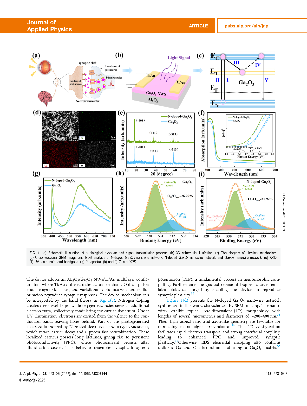
Ga₂O₃, as an ultra-wide bandgap semiconductor, possesses excellent DUV response characteristics and a high density of intrinsic defects. UV-excited photogenerated electrons in Ga₂O₃ can be partially captured by oxygen vacancies, triggering a persistent photoconductivity (PPC) effect, which allows continuous modulation of the conductance state. Regulating oxygen-vacancy defects thus enables the construction of solar-blind optoelectronic synaptic devices. While prior research has demonstrated Ga₂O₃ thin-film and nanowire-based devices, thin-film fabrication methods are complex and limited in performance, whereas nanowire-based devices exhibit enhanced synaptic plasticity due to superior optoelectronic tunability, high surface-to-volume ratio, and efficient carrier transport. However, the intrinsic oxygen-vacancy concentration in Ga₂O₃ is relatively low, making it difficult to achieve high-performance synaptic behavior solely through natural defects. Controllable defect engineering—such as doping with metals (Cu, Sn) or nitrogen (N)—can effectively tune oxygen-vacancy concentration and energy levels while maintaining high crystalline quality, with N-doping offering superior controllability and simpler operation.
Based on this, the present study focuses on N-doped Ga₂O₃ nanowire network-based solar-blind optoelectronic synaptic devices. Devices were fabricated via PECVD, and the effects of element doping on photoelectrical performance and synaptic behavior were analyzed. Furthermore, their potential applications in neuromorphic computing and optical encryption were explored, providing guidance for the development and deployment of next-generation high-performance solar-blind optoelectronic synaptic devices.
Abstract
Optoelectronic synapses use optical signals as modulation inputs and offer advantages such as low-power consumption, non-contact operation, and high parallelism. However, devices operating in the visible and near-infrared regions are susceptible to ambient light interference, leading to signal distortion and high background noise. In contrast, optoelectronic synaptic devices working in a solar-blind region are impervious to external ambient interference, enabling them to achieve stable and high-fidelity signal transmission effectively. Ga2O3 as a wide bandgap with inherent oxygen-vacancy defects has strong deep-ultraviolet light sensitivity, making it an ideal material for solar-blind optoelectronic synapses. Here, high-performance solar-blind synaptic devices were prepared using nanowire network interfacial effects and nitrogen doping to modulate oxygen vacancies. Notably, the paired-pulse facilitation index increased by approximately 1.2 fold after doping. In handwritten digit recognition experiments, the recognition accuracy of the doped device exceeded 90%, representing an improvement of nearly 15% compared to the undoped counterpart. Furthermore, leveraging its enhanced light perception and strong memory characteristics, a precise optical encryption communication scheme with strong anti-interference capability was also designed. The optoelectronic synaptic devices based on element regulated Ga2O3 nanowire network provide a new way for the development of the next generation of high-performance solar-blind optoelectronic neuromorphic systems.
Conclusion
In conclusion, a high-performance solar-blind optoelectronic synaptic device based on N-doped Ga2O3 nanowire network was constructed in this work by modulating oxygen vacancies. The doped devices exhibit higher performance parameters in both optoelectronic and neural morphology applications. The paired-pulse facilitation index increased from 140% to 160% after doping, exhibiting stronger synaptic plasticity. The MNIST recognition accuracy of 90% significantly surpassing the 78% accuracy of the undoped device, showing its superior image retention and short-term memory. A dynamic key synchronization scheme was built using the device’s tunable transient and self-erasing features. Meanwhile, its solar-blind response enables strong immunity to interference and information leakage, ensuring high security and antieavesdropping capability. It highlights the application potential of Ga2O3 nanowire network-based synaptic devices in integrated neuromorphic computing and secure communication.
Project Support
This work was supported by the Scientific Research Fund of Zhejiang Provincial Education Department (23060158-F), Zhejiang Provincial Natural Science Foundation of China (LQ24F040002), National Natural Science Foundation of China (Nos. 62374147, 62274148, and 62304205), Joint Funds of the National Natural Science Foundation of China (No. U23A20349), and Science Foundation of Zhejiang Sci-Tech University (No. 24062240-Y).
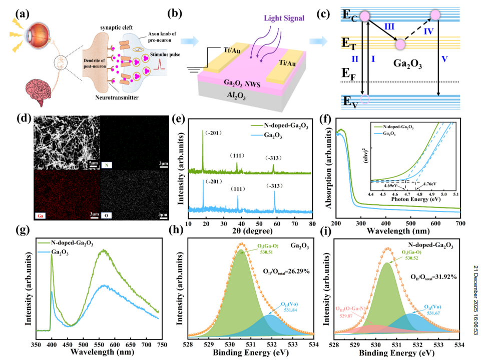
FIG.1 (a) Schematic illustration of a biological synapse and signal transmission process. (b) 3D schematic illustration. (c) The diagram of physical mechanism. (d) Cross-sectional SEM image and EDS analysis of N-doped Ga2O3 nanowire network. N-doped Ga2O3 nanowire network and Ga2O3 nanowire network: (e) XRD. (f) UV–vis spectra and bandgaps. (g) PL spectra. (h) and (i) O1s of XPS.
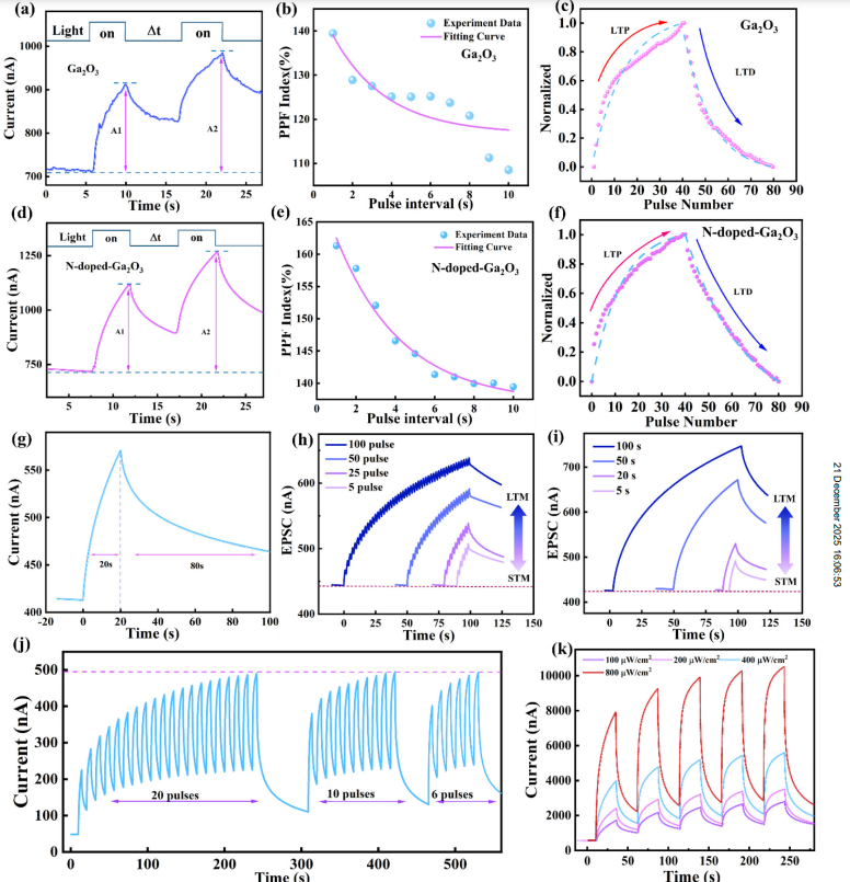
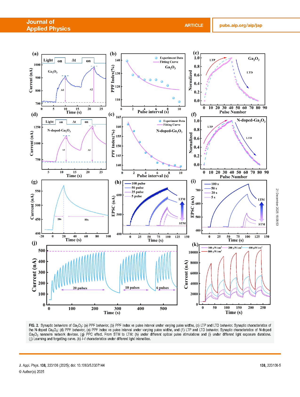
FIG.2 Synaptic behaviors of Ga2O3: (a) PPF behavior, (b) PPF index vs pulse interval under varying pulse widths, (c) LTP and LTD behavior. Synaptic characteristics of the N-doped Ga2O3: (d) PPF behavior, (e) PPF index vs pulse interval under varying pulse widths, and (f) LTP and LTD behavior. Synaptic characteristics of N-doped Ga2O3 nanowire network devices. (g) PPC effect. From STM to LTM: (h) under different optical pulse stimulations and (i) under different light exposure durations. (j) Learning and forgetting curve. (k) I–t characteristics under different light intensities.
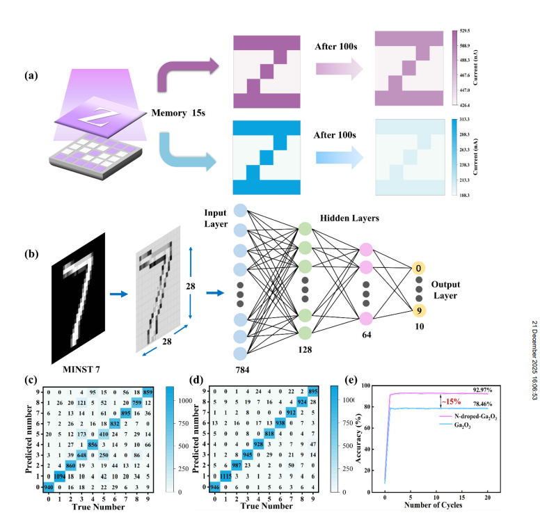
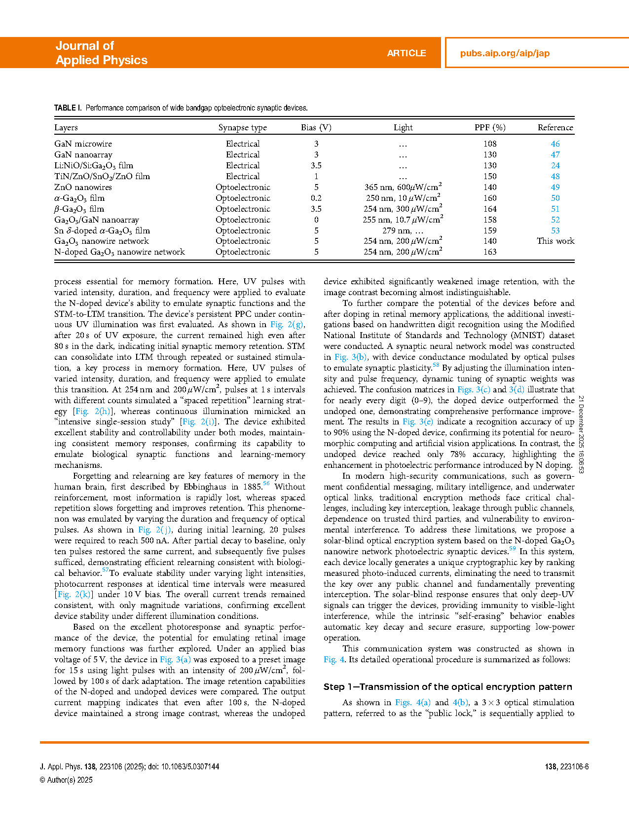
FIG.3 (a) Image memory results of N-doped and undoped Ga2O3 nanowire network devices. (b) Schematic diagram of the Backpropagation Neural Network (BPNN) used for MNIST handwritten digit recognition. Confusion matrix in the MNIST recognition task for (c) undoped and (d) N-doped device. (e) Accuracy and loss function curves in the MNIST recognition task for undoped and N-doped synaptic devices.
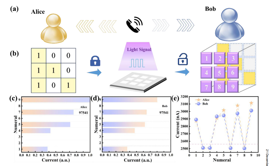
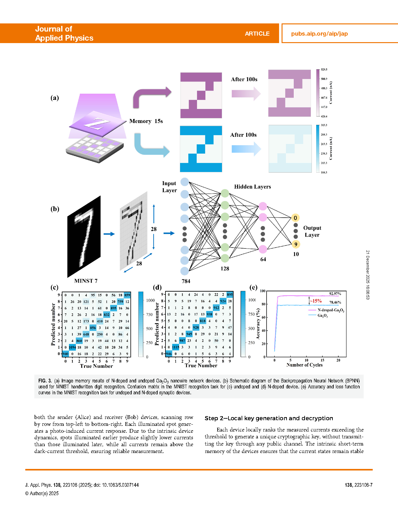
FIG.4 (a) Process diagram and (b) principle diagram of optical communication between Alice and Bob. (c) Password sequence obtained from Alice to Bob. (d) Password sequence obtained from Bob to Alice. (e) Matching graph of password strength.
DOI:
doi.org/10.1063/5.0307144