Paper Sharing
【Member Papers】Enhanced OH− transport and storage in oxygen vacancy-enriched α-Ga₂O₃ shells constructed on GaN nanowires for supercapacitor
日期:2025-12-24阅读:502
Researchers from the Xiamen University of Technology have published a dissertation titled "Enhanced OH− transport and storage in oxygen vacancy-enriched α-Ga2O3 shells constructed on GaN nanowires for supercapacitor" in Chemical Engineering Journal.
Background
Gallium oxide (Ga₂O₃) is a representative ultra-wide bandgap semiconductor that has been extensively investigated for applications in high-power electronics, solar-blind ultraviolet photodetectors, transparent conductive layers, sensors, and photoelectrochemical systems. Recently, Ga₂O₃ has also attracted growing interest as an electrode material for lithium/sodium-ion batteries and supercapacitors due to its high theoretical capacity. However, the practical electrochemical performance of Ga₂O₃ is strongly influenced by its intrinsic point defects, such as oxygen vacancies and gallium vacancies. While these defects degrade electrical conductivity by acting as carrier scattering centers, they simultaneously provide active sites for ion adsorption and redox reactions, offering opportunities for energy storage applications. In particular, α-Ga₂O₃ exhibits a high density of intrinsic point defects and relatively low electron mobility, which limits charge transport. To overcome this limitation, hybrid strategies that combine Ga₂O₃ with highly conductive materials have been explored to enhance electrical conductivity while retaining defect-related electrochemical activity. Previous studies demonstrated that composite structures, such as α-Ga₂O₃/GaN on carbon cloth, can effectively decouple charge transport and electrochemical activity, where Ga₂O₃ provides redox-active sites and GaN serves as a fast electron transport pathway. Despite these advances, the fundamental charge storage mechanisms in α-Ga₂O₃—including surface redox reactions, bulk ion migration, and the specific role of point defects—remain insufficiently understood. Moreover, optimizing microstructure to balance defect density, electron transport, and ion diffusion is still a critical challenge. Nanostructuring is a promising approach, as it increases surface active sites and shortens transport paths for both ions and electrons. Against this background, the present work focuses on engineering nanostructured α-Ga₂O₃ shells on GaN nanowires supported by carbon cloth. By controlling air-annealing conditions, a highly defect-rich α-Ga₂O₃ layer is formed, enabling systematic investigation of defect-assisted charge storage mechanisms. This study aims to clarify the role of intrinsic oxygen vacancies in electrochemical performance and to provide a rational design strategy for high-performance Ga₂O₃-based supercapacitors.
Abstract
Ga2O3 is an important ultra-wide bandgap semiconductor which has emerged as an attractive electrode material for energy storage devices in recent years. In this study, a highly defective α-Ga2O3 shell was developed on GaN nanowires (NWs) anchored on carbon cloth (CC) via an Au-assisted chemical vapor deposition (CVD) method followed by an air-annealing under 500 °C. The α-Ga2O3 shell endowed the electrode with a high electron density (ND) and facilitated the ion transport/storage, and the GaN NW cores worked as highways enabling fast electron transport. A symmetric aqueous SC using the GaN NWs@α-Ga2O3 core-shell structure as the electrode material delivered a capacitance (Csingle) of 1352.81 mF cm−2, an energy density (E) of 18.87 Wh kg−1, and a power density (P) of 5.44 W kg−1 at 0.5 mA cm−2. The Csingle, E, and P under 10 mA cm−2 were 1146.13 mF cm−2, 1.91 Wh kg−1, and 245.95 W kg−1, respectively, with 85.54 % of the capacitance retained after 20,000 cycles. A redox reaction of OH−/*OH ions in the α-Ga2O3 shell was revealed. The high density of oxygen vacancies (VO) in the α-Ga2O3 shell were identified to play a significant role in the electrochemical performances by promoting electrical conductivity, serving as active sites to dissociate H2O and absorb OH− ions on the surface, and facilitating the diffusion of OH−/*OH ions in the bulk of the α-Ga2O3. The current work provides deep insights on the charge storage mechanism of the α-Ga2O3 and offers a practical strategy to develop α-Ga2O3-based energy storage devices.
Highlight
• A supercapacitor electrode with GaN NWs@α-Ga2O3 structure on carbon cloth was synthesized.
• A redox reaction of OH−/*OH occurred in the α-Ga2O3 shell during charging/discharging process.
• VO in the α-Ga2O3 shell facilitated the surface adsorption of OH− and bulk diffusion of OH−/*OH.
• VO in the α-Ga2O3 shell contributes to the improvement of the electrical conductivity.
Conclusion
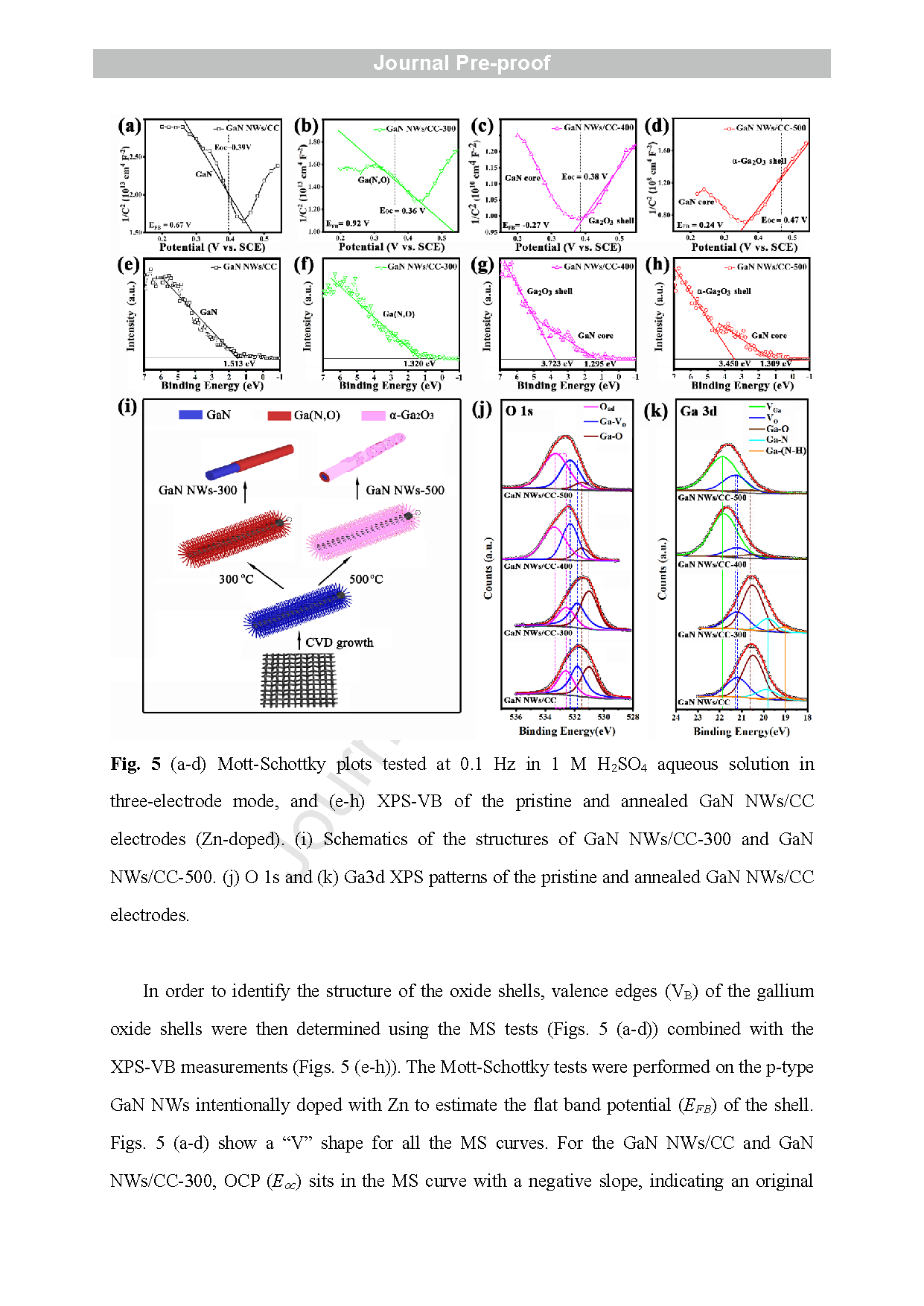
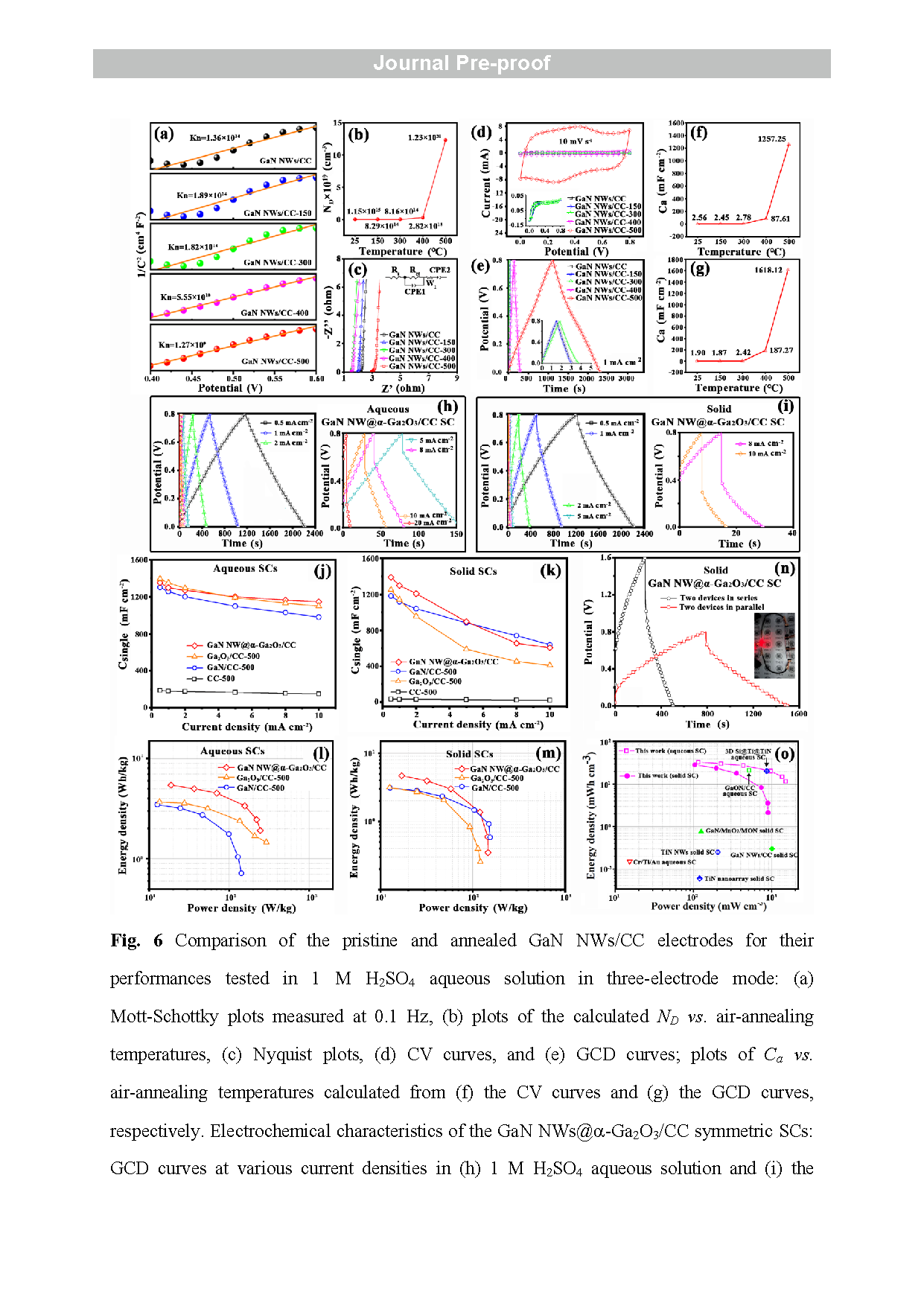
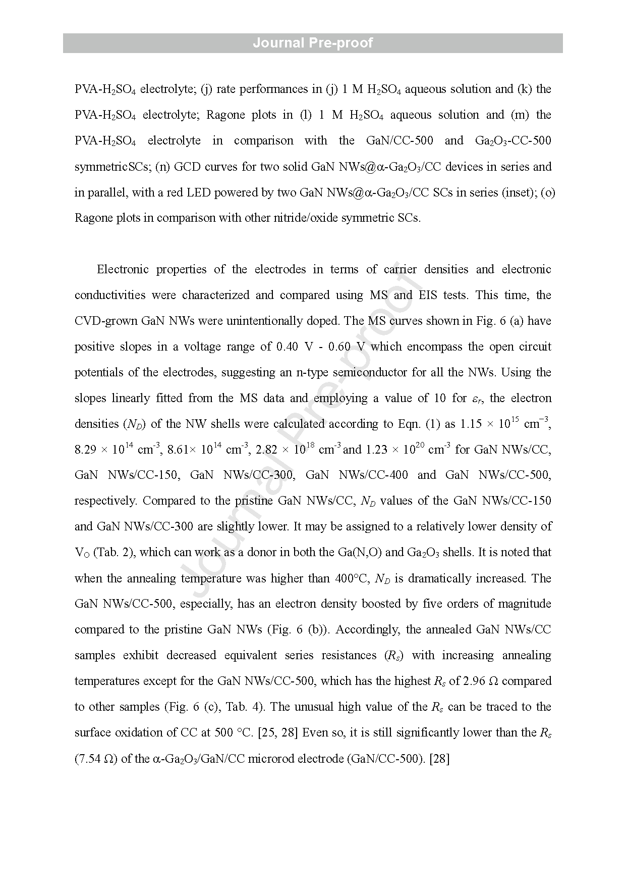
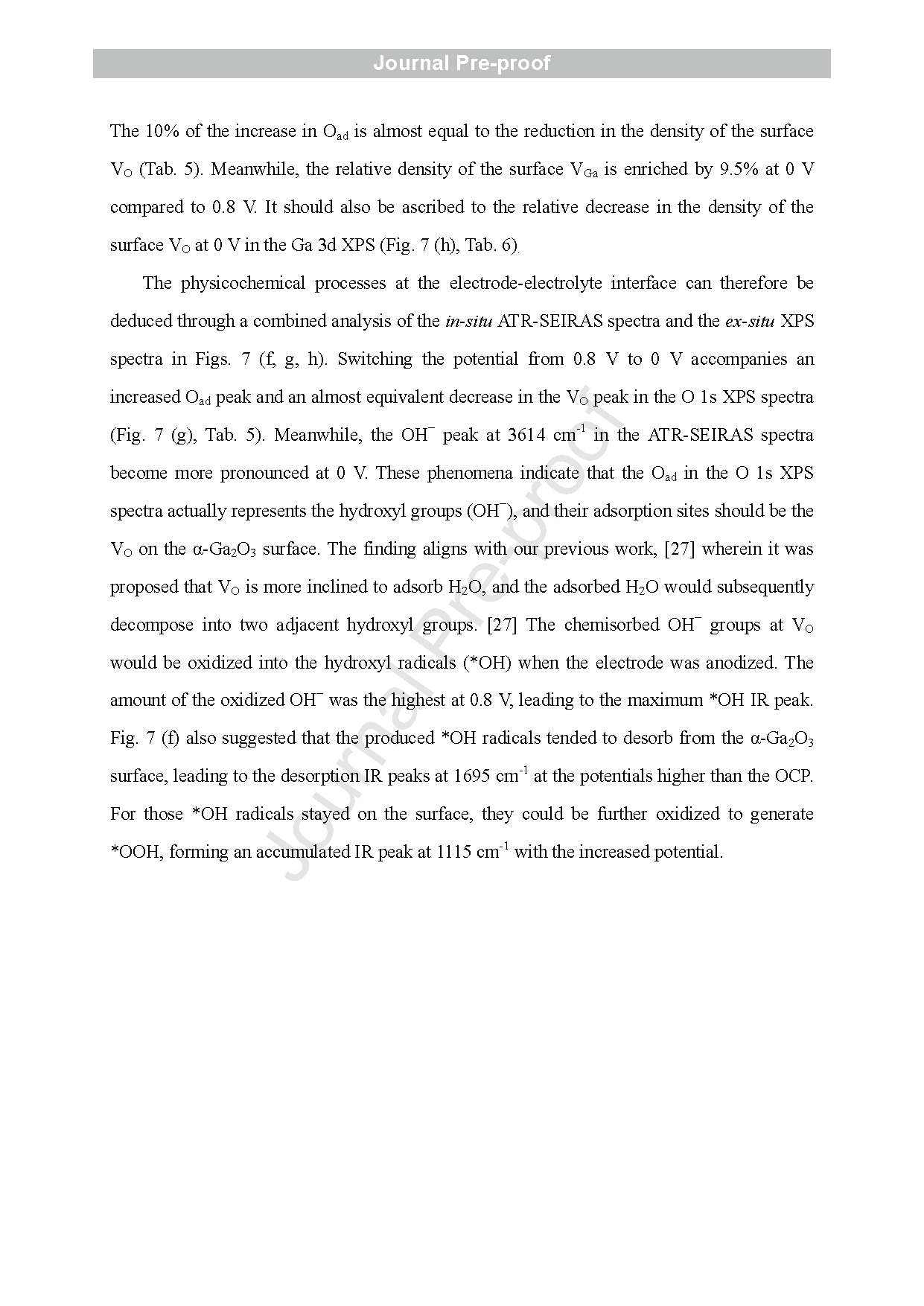
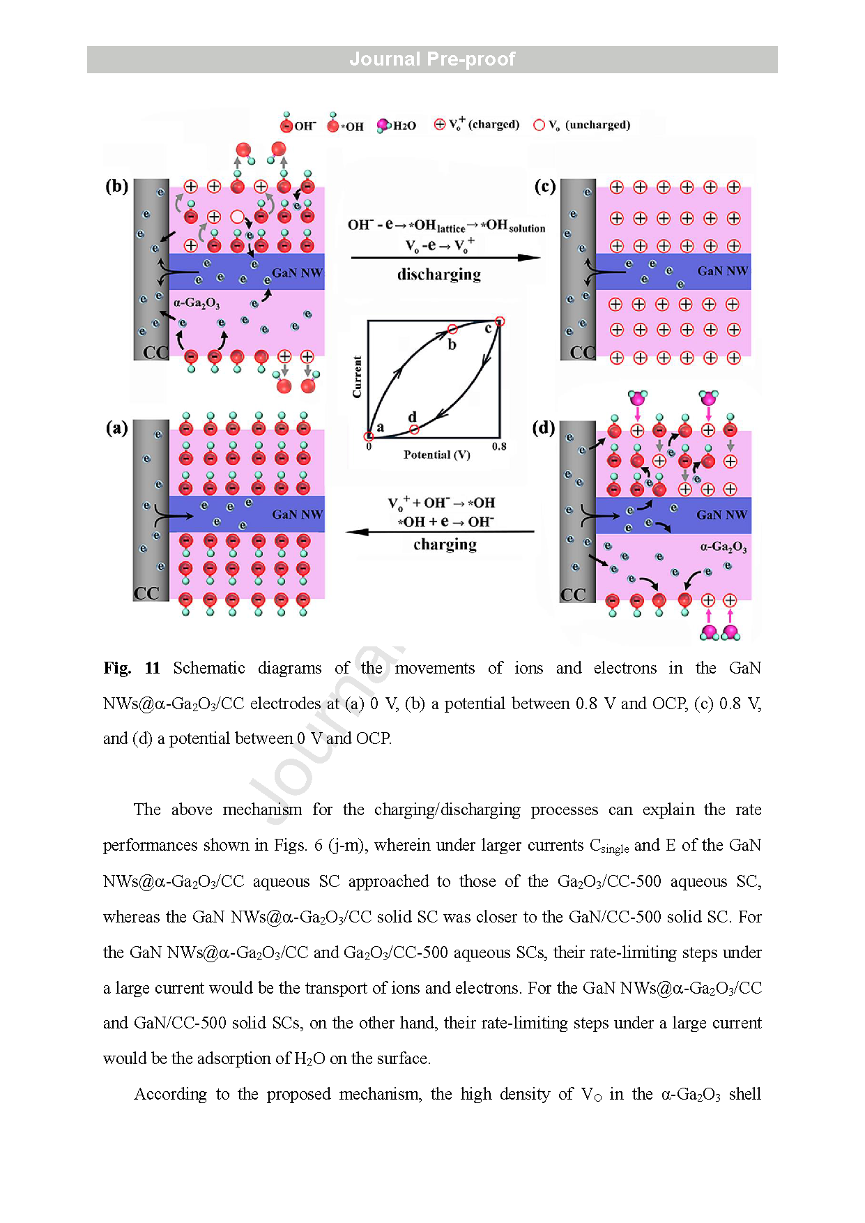
In this article, a GaN NWs@α-Ga2O3 core -shell structure anchored on CC was developed by growing GaN NWs on CC using an Au -assisted CVD method followed by air -annealing. The microstructures of the annealed GaN NWs/CC electrodes under different temperatures were characterized and compared using SEM, TEM, MS, and XPS. A highly defective α-Ga2O3 shell enriched with VO was confirmed on the surface of the GaN NWs in the electrode air -annealed at 500 ° C. The electrode with the GaN NWs@α-Ga2O3 core -shell structure exhibited the highest electron density and specific capacitance. After excluding the contribution of CC, the aqueous GaN NWs@α-Ga2O3/CC symmetric SC delivered an energy density (E) of 18.87 Wh kg-1 and a power density (P) of 5.44 W kg-1 at 0.5 mA cm-2 . At a higher current density of 10 mA cm-2 , E and P of the aqueous GaN NWs@α-Ga2O3/CC SC are 1.91 Wh kg-1 and 245.95 W kg-1 , respectively. The aqueous GaN NWs@α-Ga2O3/CC SC also manifested a high cycling stability by keeping 85.54 % of the initial capacitance s after 20000 cycles at 10 mA cm-2 . Using quantitative analysis of the CV scanning combined with i n situ ATR -SEIRAS and ex situ XPS testing, the charge storage mechanism of the GaN NWs@α-Ga2O3/CC was identified as the adsorption of the OH− ions at VO sites on the surface of the α-Ga2O3, the redox reaction of OH− /*OH ions in the α-Ga2O3, and the diffusion of the OH− /*OH ions along the VO in the α-Ga2O3 shell. The last step was found to dominate the electrochemical performances of the GaN NWs@α-Ga2O3/CC electrode . Detailed DFT calculations provided theoretical insights into the above -mentioned mechanism. Our finding s not only provide deeper understanding of the charge storage mechanism of α-Ga2O3, but also offer a promising strategy to design more α-Ga2O3 -based energy -storage devices with higher performance in the future .
Project Support
This work was supported by the National Natural Science Foundation of China (Nos. 52250710159, 52401023), the Natural Science Foundation of Fujian Province (No. 2021J011210).
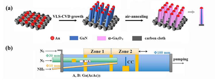
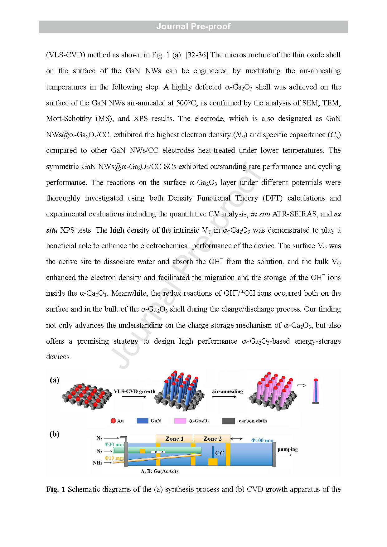
Fig. 1 Schematic diagrams of the (a) synthesis process and (b) CVD growth apparatus of the GaN NWs@ a -Ga2O3/CC electrode
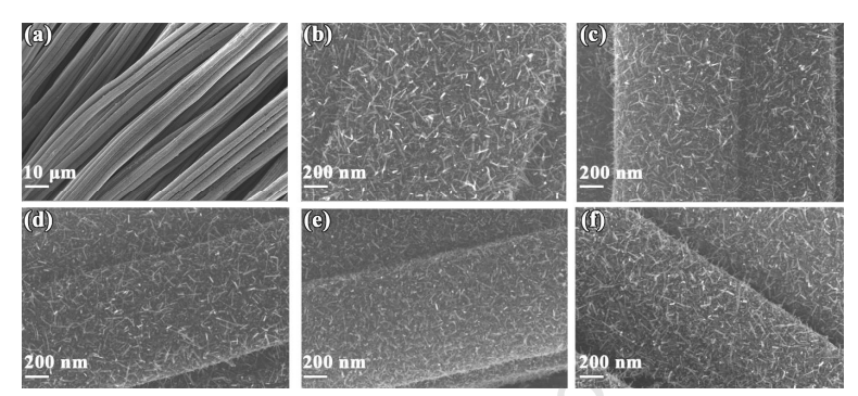
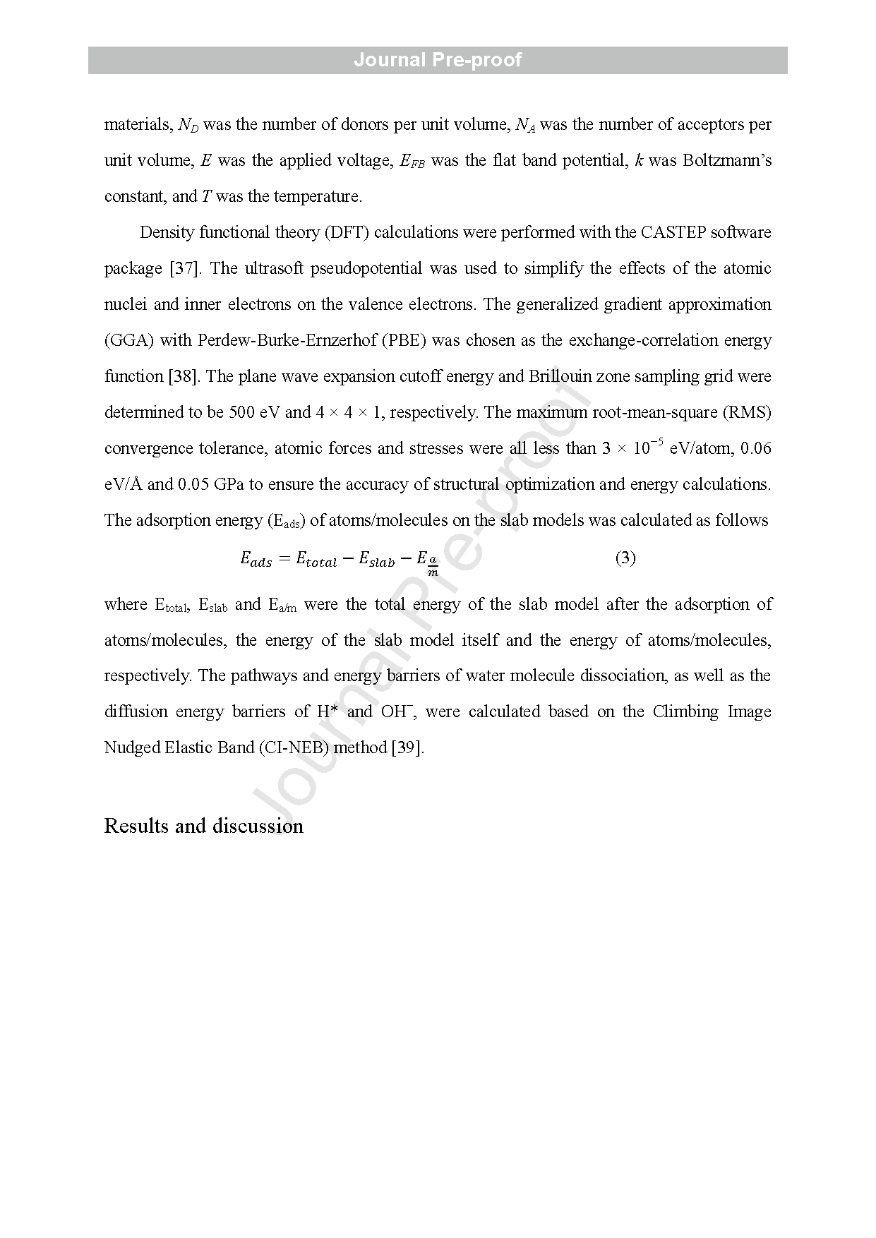
Fig. 2 SEM images of (a and b) GaN NWs/CC, (c) GaN NWs/CC -150, (d) GaN NWs/CC -300, (e) GaN NWs/CC -400, (f) GaN NWs/CC -500
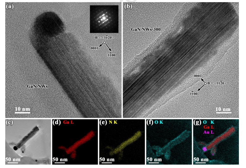
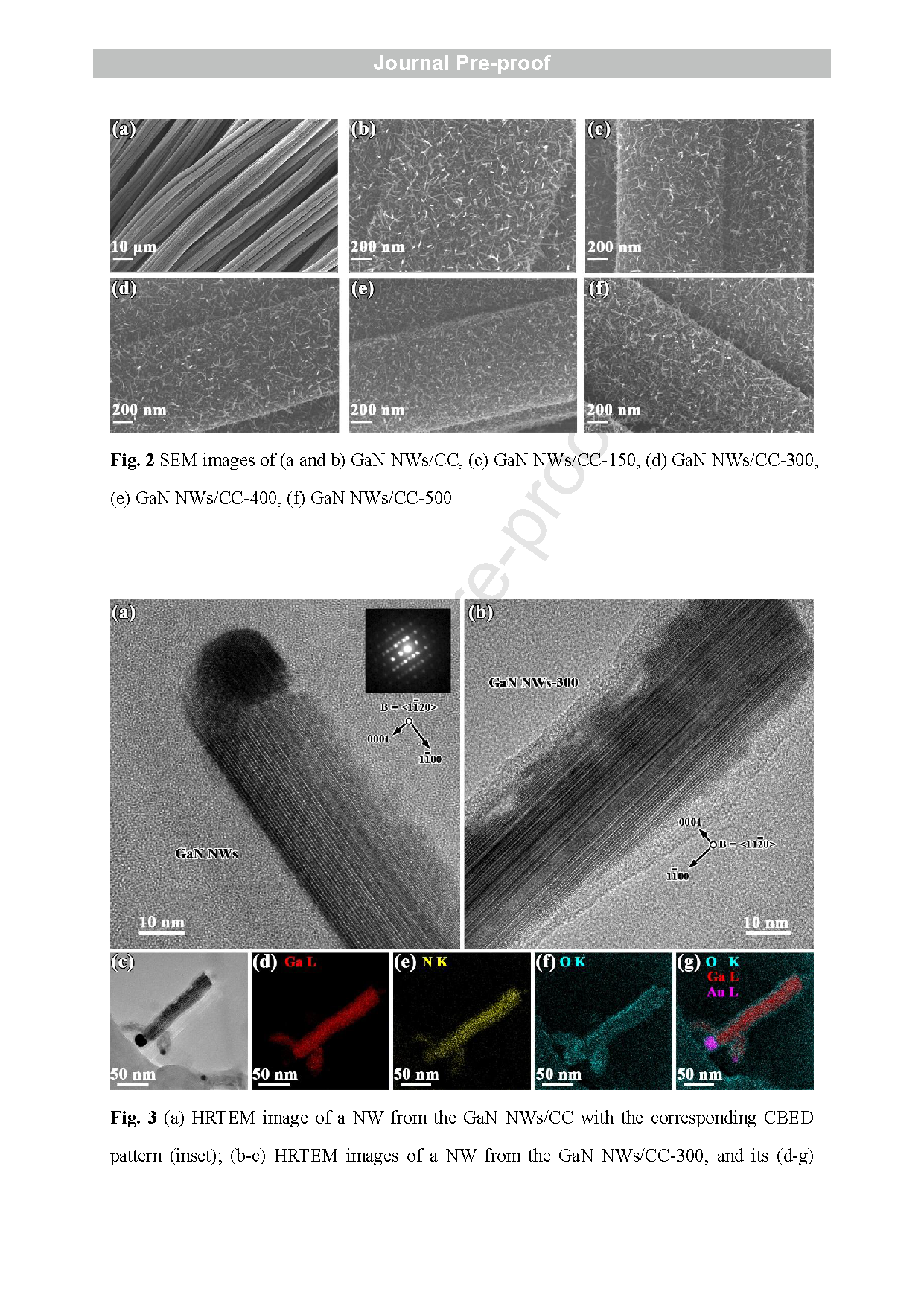
Fig. 3 (a) HRTEM image of a NW from the GaN NWs/CC with the corresponding CBED pattern (inset); (b-c) HRTEM images of a NW from the GaN NWs/CC -300, and its (d-g) EDS/STEM mappings (net intensity) for elements Ga, N, O, and O/Ga/Au, respectively.
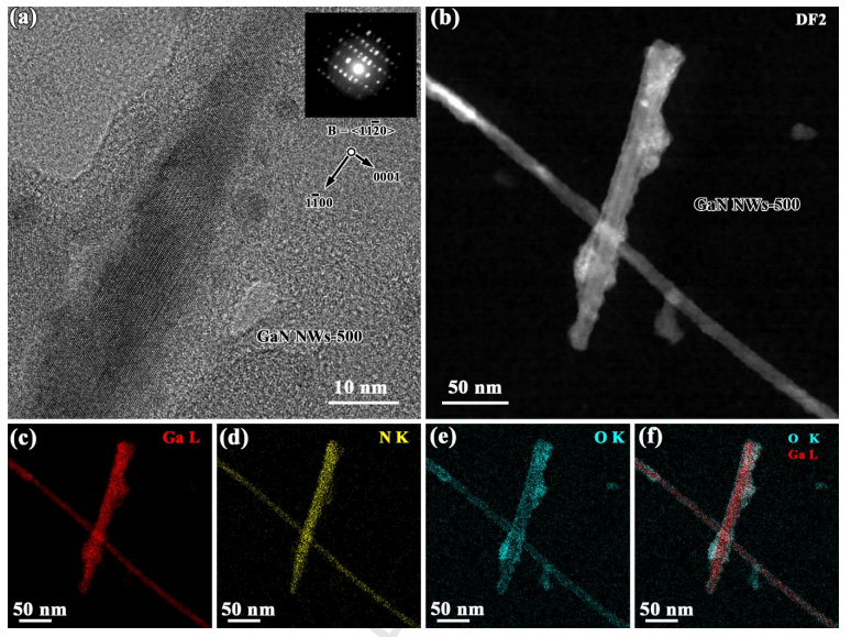
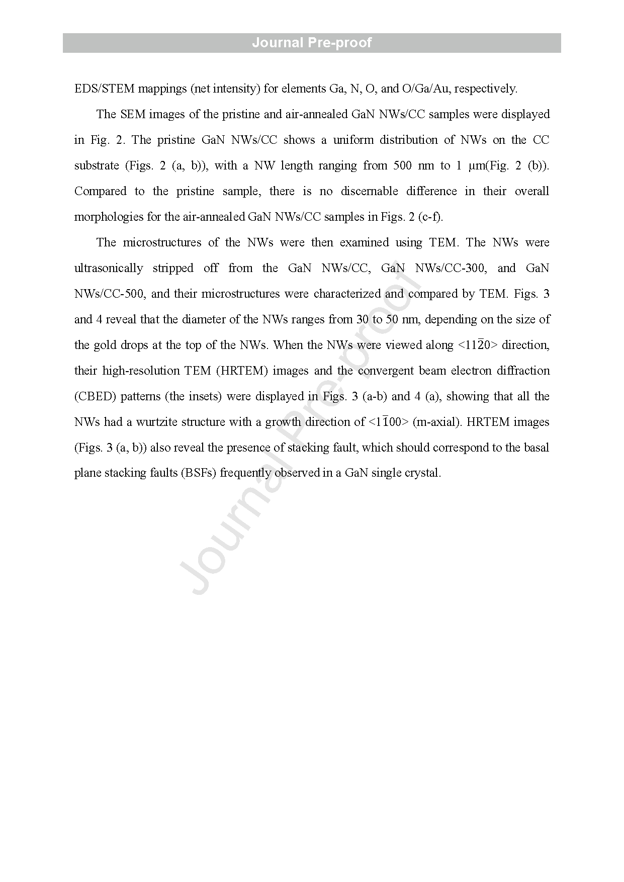
Fig. 4 (a) HRTEM image of a NW from the GaN NWs/CC-500 with the corresponding CBED pattern (inset); (b) DF -STEM image of NWs from the GaN NWs/CC-500, and their (b -f) EDS/STEM mappings (net intensity) for elements Ga, N, O, and O/Ga, respectively.
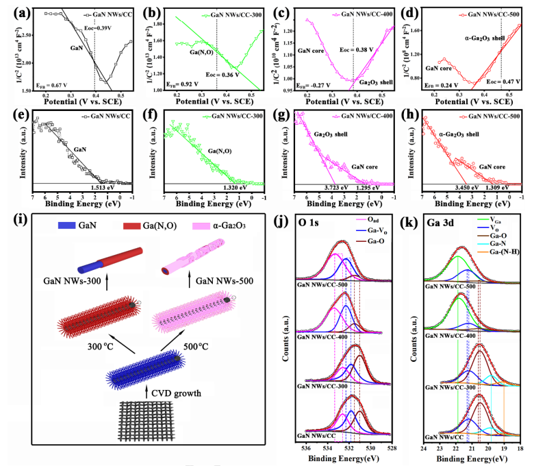
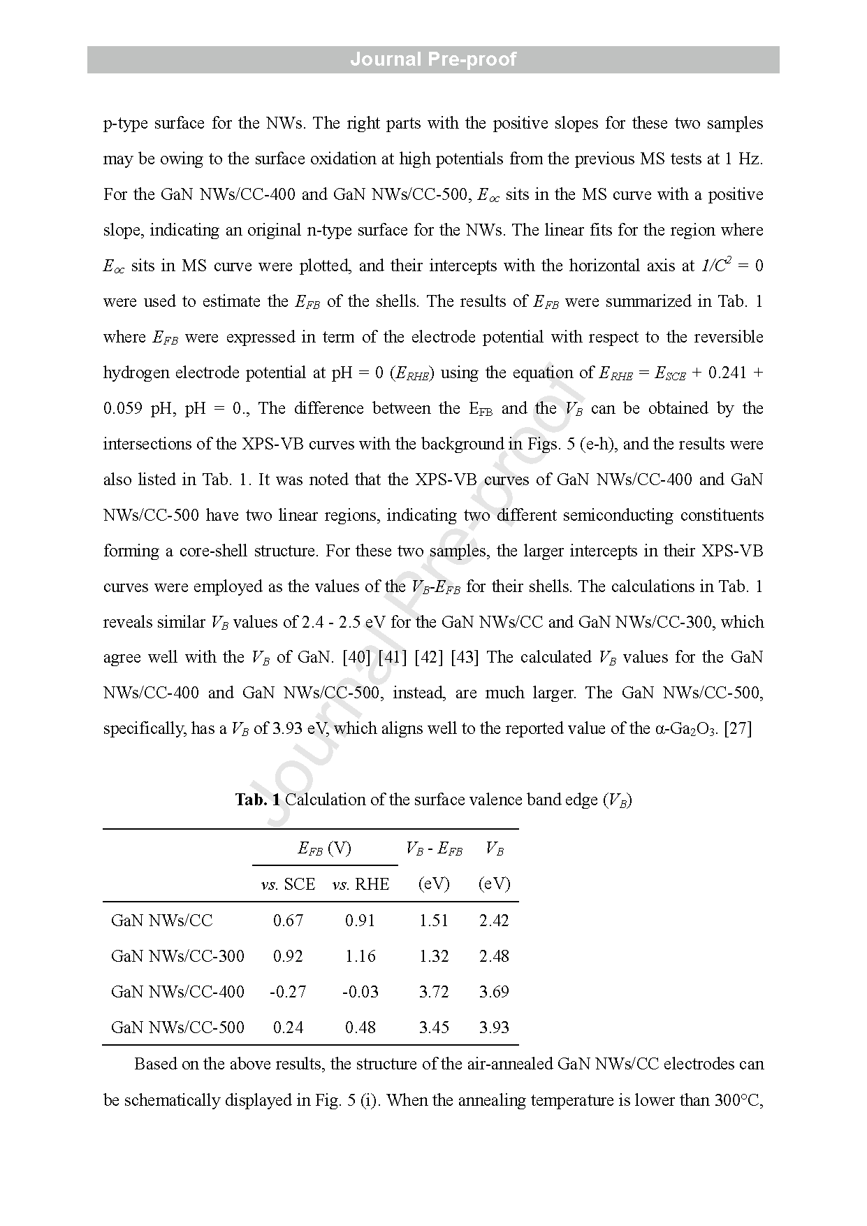
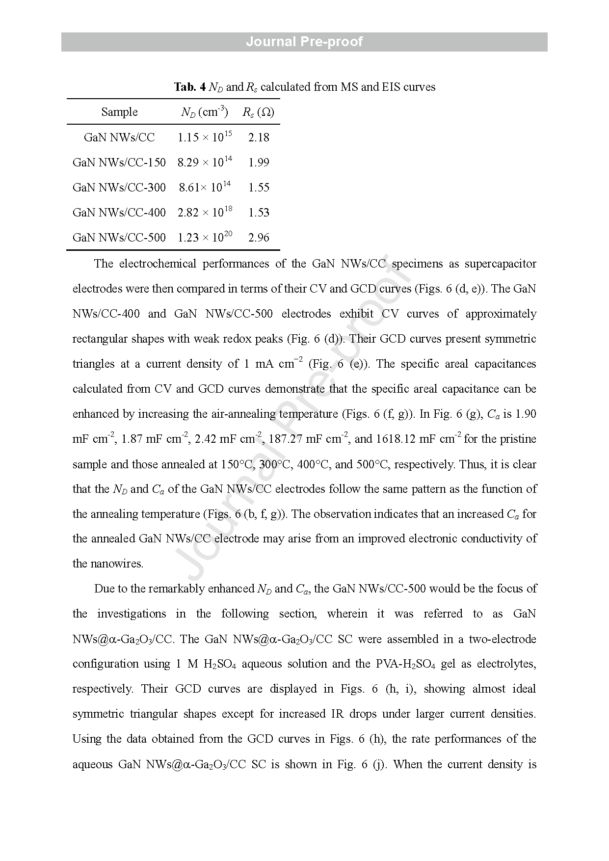
Fig. 5 (a-d) Mott -Schottky plots tested at 0.1 Hz in 1 M H2SO4 aqueous solution in three -electrode mode, and (e -h) XPS -VB of the pristine and annealed GaN NWs/CC electrodes (Zn -doped ). (i) Schematics of the structures of GaN NWs/CC -300 and GaN NWs/CC -500 . (j) O 1s and (k) Ga3d XPS patterns of the pristine and annealed GaN NWs/CC electrodes
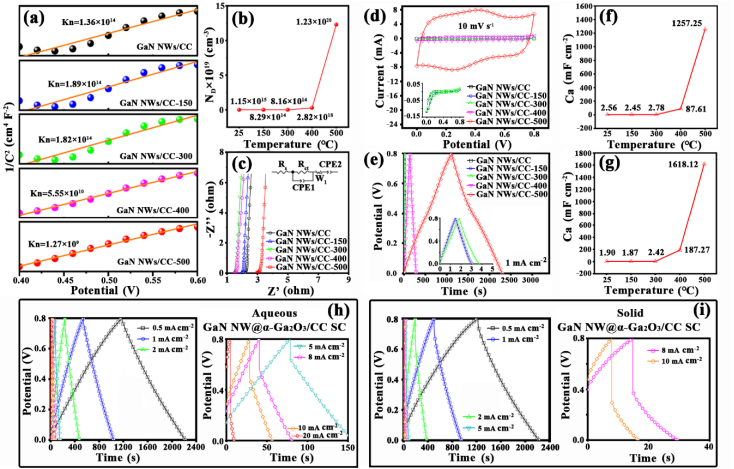
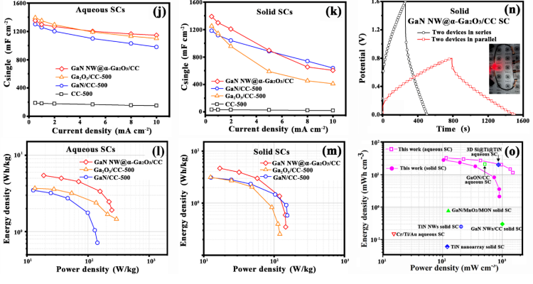
Fig. 6 Comparison of the pristine and annealed GaN NWs/CC electrodes for their performances tested in 1 M H2SO4 aqueous solution in three -electrode mode: (a) Mott-Schottky plots measured at 0.1 Hz , (b ) plots of the calculated ND vs . air -annealing temperature s, (c) Nyquist plot s, (d) CV curves, and ( e ) GCD curves; plots of Ca vs. air -annealing temperatures calculated from (f) the CV curves and ( g ) the GCD curves, respectively. Electrochemical characteristics of the GaN NWs@ a-Ga2O3/CC symmetric SC s: GCD curves at various current densities in ( h) 1 M H2SO4 aqueous solution and ( i) the PVA - H2SO4 electrolyte; (j) rate performances in (j) 1 M H2SO4 aqueous solution and ( k) the PVA - H2SO4 electrolyte ; Ragone plots in ( l ) 1 M H2SO4 aqueous solution and ( m) the PVA - H2SO4 electrolyte in comparison with the GaN/CC -500 and Ga2O3 -CC -500 symmetricSC s ; ( n) GCD curves for two solid GaN NWs@ a-Ga2O3/CC devices in series and in parallel, with a red LED powered by two GaN NWs@a-Ga2O3/CC SCs in series (inset ) ; ( o ) Ragone plots in comparison with other nitride/oxide symmetric SCs.
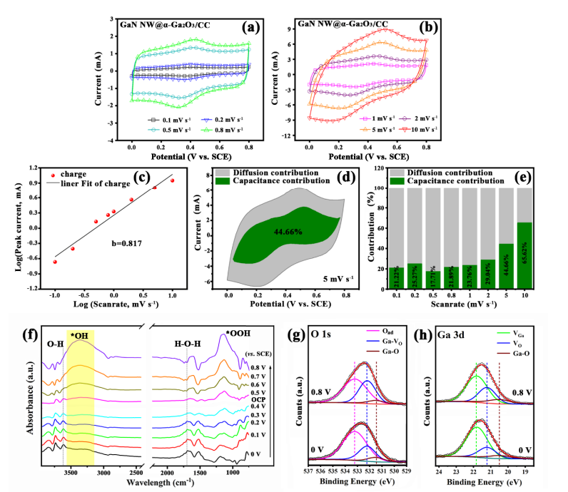
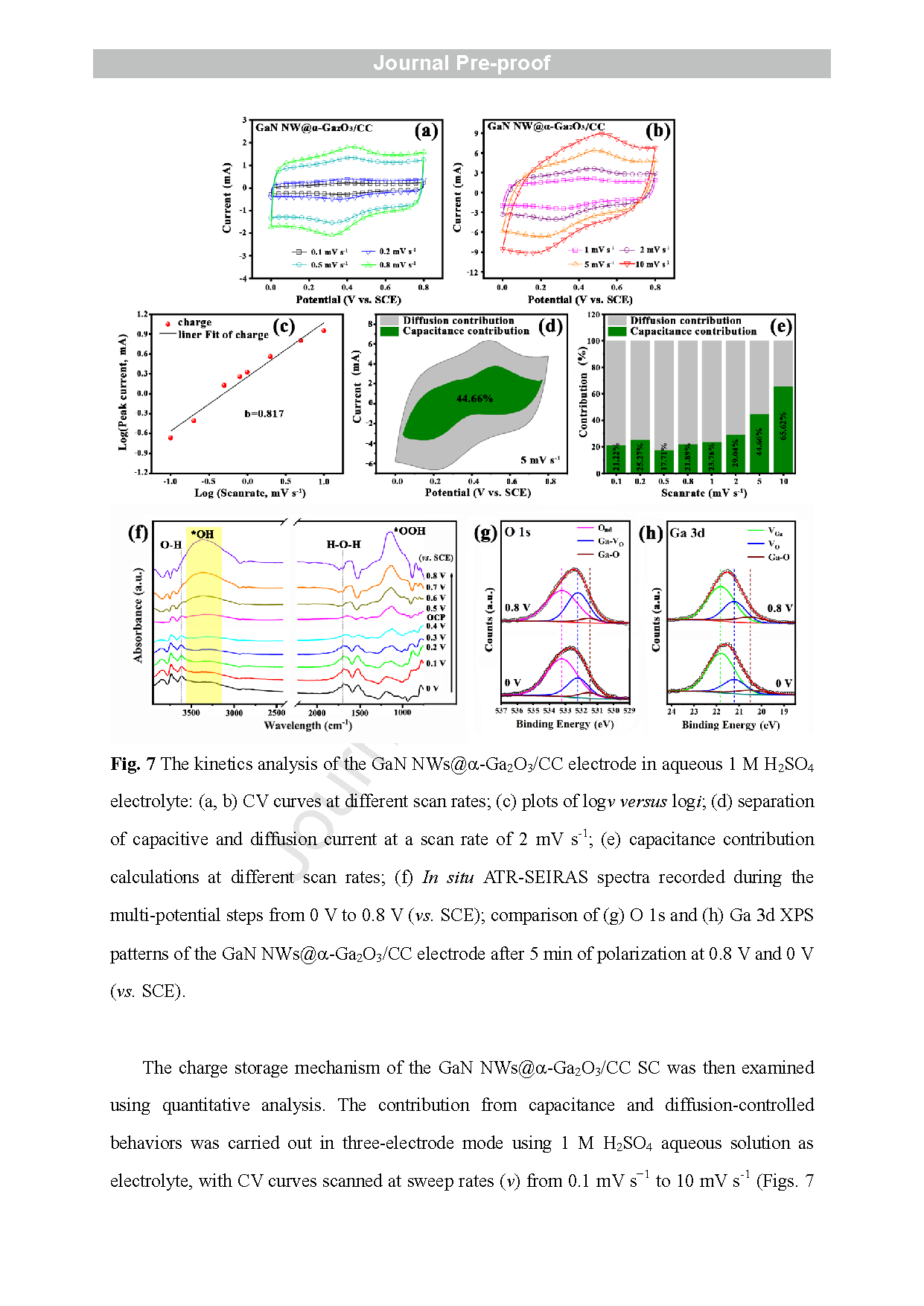
Fig . 7 The kinetics analysis of the GaN NWs@ a-Ga2O3/CC electrode in aqueous 1 M H2SO4 electrolyte : (a, b) CV curves at different scan rates ; (c) plots of log ν versus log i; (d) separation of capacitive and diffusion current at a scan rate of 2 mV s-1 ; (e) capacitance contribution calculations at different scan rates ; ( f) In situ ATR -SEIRAS spectra recorded during the multi -potential steps from 0 V to 0.8 V (vs. SCE); comparison of ( g) O 1s and ( h ) Ga 3d XPS patterns of the GaN NWs@ a-Ga2O3 CC electrode after 5 min of polarization at 0.8 V and 0 V (vs. SCE) .
Fig. 8 (a) Schematic diagram of the optimized configuration of bulk a-Ga2O3 crystal and the location of VO. (b, c) Energy band diagrams and (d, e) PDOS diagrams of a-Ga2O3 and a-Ga2O3 - VO .
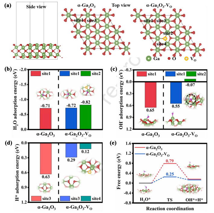
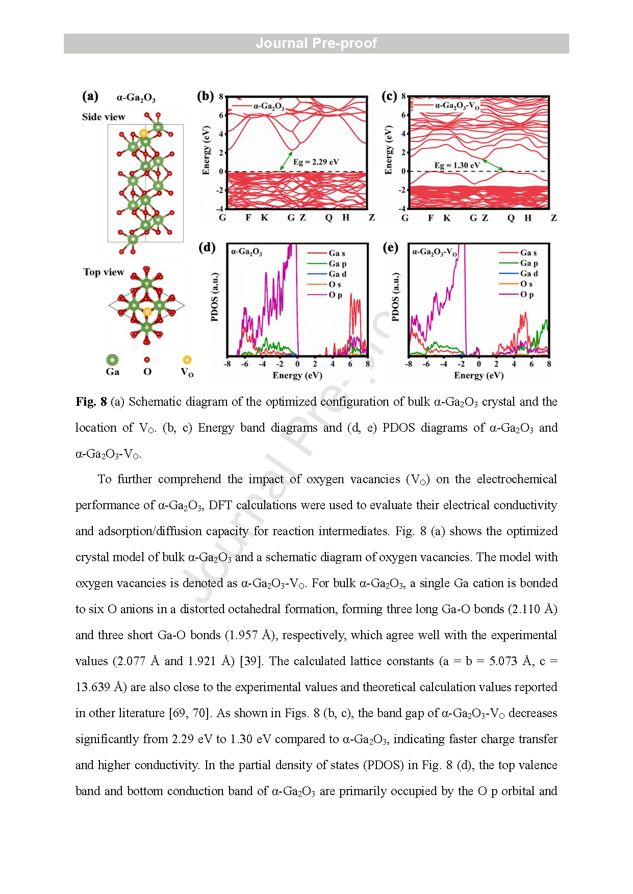
Fig. 9 (a) Optimized configurations of a-Ga2O3 and a-Ga2O3 - VO slab models, with adsorption locations marked. Adsorption energies of (b) H2O, (c) OH − and (d) H* at different adsorption sites. (e) Energy barrier diagram for water dissociation.
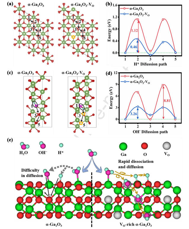
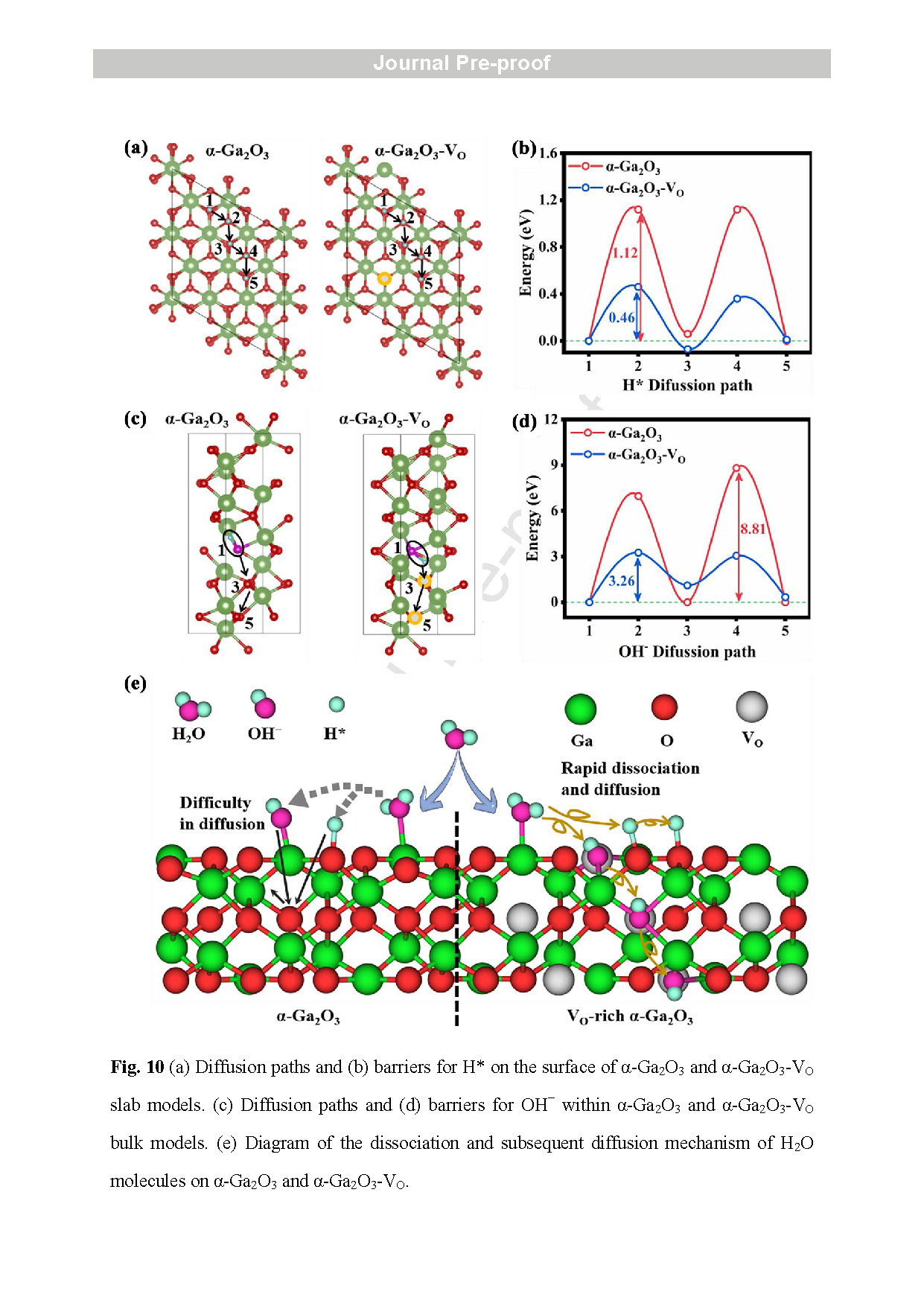
Fig. 10 (a) Diffusion paths and (b) barriers for H* on the surface of a-Ga2O3 and a-Ga2O3 - VO slab models. (c) Diffusion paths and (d) barriers for OH− within a-Ga2O3 and a-Ga2O3 - VO bulk models. (e) Diagram of the dissociation and subsequent diffusion mechanism of H2O molecules on a-Ga2O3 and a-Ga2O3 - VO .
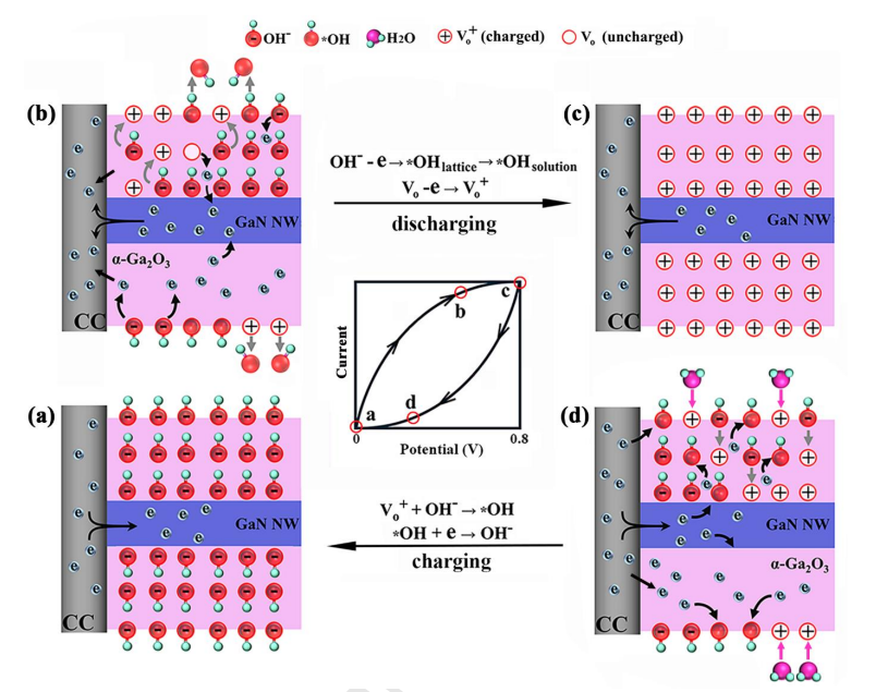
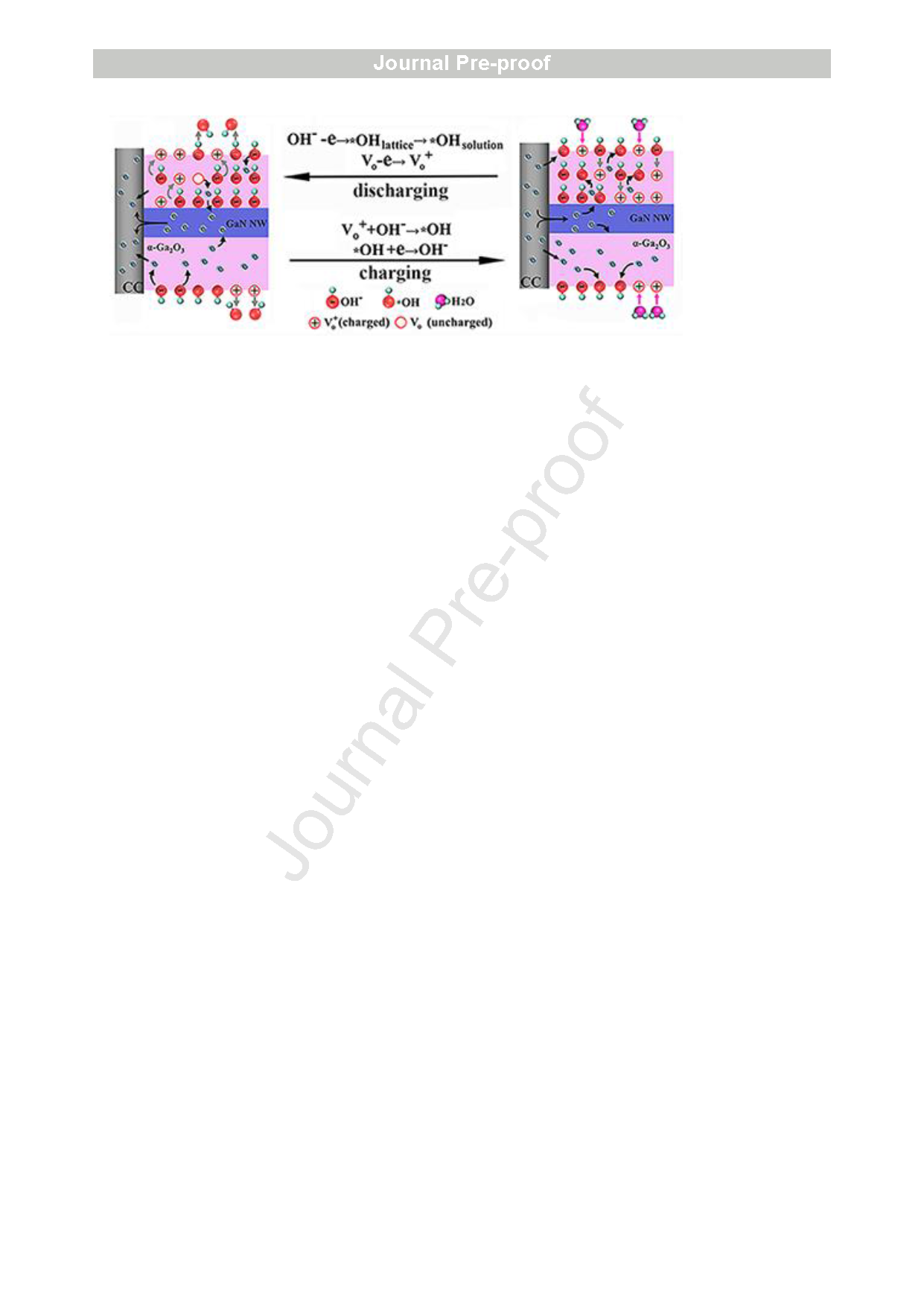
Fig. 11 Schematic diagrams of the movements of ions and electrons in the GaN NWs@ a-Ga2O3/CC electrodes at (a) 0 V, (b) a potential between 0.8 V and OCP, (c) 0.8 V, and (d) a potential between 0 V and OCP.
DOI:
doi.org/10.1016/j.cej.2025.172009