Paper Sharing
【Member Papers】Ultrahigh-efficiency solar-blind ultraviolet detection with a β-Ga₂O₃/Si heterojunction
日期:2025-12-24阅读:515
Researchers from the Dalian University of Technology have published a dissertation titled "Ultrahigh-efficiency solar-blind ultraviolet detection with a β-Ga2O3/Si heterojunction" in Applied Physics Letters.
Project support
This research was funded by the Liaoning Province Natural Science Foundation Joint Fund (Doctoral Research Initiation Project), Grant No. 2023-BSBA-028; the Fundamental Research Funds for the Central Universities, Grant No. DUT24BS008; the Guangdong Basic and Applied Basic Research Foundation, Grant No. 2023A1515110064; the National Key Research and Development Program of China, Grant No. 2023YFB4503003; and the National Natural Science Foundation of China, Grant Nos. 62304030 and 62104024.
Background
Taking advantage of its low environmental noise, high sensitivity, and all-weather operational capability, solar-blind ultraviolet (SBUV, 200–280 nm) detection technology has showcased tremendous potential for a wide array of applications, spanning space exploration, projectile early warning, secure communications, and beyond. Given the feeble intensity of SBUV signals, SBUV photodetectors (PDs) have to exhibit high photoelectric conversion efficiency. At present, commercial PDs are mainly constructed using silicon (Si). Nevertheless, Si possesses a bandgap of only 1.12 eV, its substantial energy mismatch with the SBUV region (4.43–6.20 eV) significantly curtails the photoelectric conversion efficiency of Si-based PDs. Furthermore, the sensitivity of Si toward non-SBUV signals presents a substantial challenge as well. Consequently, over the past decade, researchers have increasingly focused their efforts on ultrawide bandgap materials, including (β gallium oxide) β-Ga2O3, AlxGa1-xN, MgxZn1-xO, AlxGa1-xO, and diamond. However, these ultrawide bandgap materials are not perfect candidates, for example, the high-temperature (over 1350 °C) processes essential for the epitaxy of AlxGa1xN substantially elevate the thermal budget the bandgap of diamond (5.47 eV, 227 nm) lies close to the edge of the SBUV region, limiting its applicability;10 the preparation processes for MgxZn1-xO and AlxGa1-xO remain immature and β-Ga2O3 suffers from low electron mobility and the lack of well-established p-type doping. Furthermore, Si, as the most successfully commercialized semiconductor, has built up a solid industrial foundation over the past decades. This grants Si unparalleled advantages in subsequent signal readout, device integration, and packaging processes. In light of these factors, integrating Si with ultrawide bandgap materials to leverage the inherent physical properties of Si and offset the deficiencies of ultrawide bandgap materials will not only boost the performance of PDs but also facilitate the seamless implementation of subsequent technologies
Abstract
To overcome the limitations of low responsivity (R) and suboptimal spectral selectivity inherent in silicon (Si)-based solar-blind ultraviolet (SBUV) photodetectors (PDs), as well as the challenges posed by the low electron mobility and polycrystalline structure of heteroepitaxial β gallium oxide (β-Ga2O3), a high-electron-mobility PD utilizing a β-Ga2O3/Si heterojunction is developed. In this PD, β-Ga2O3 serves as the SBUV absorption layer, capitalizing on its high responsivity and spectral selectivity, while Si acts as the photogenerated electron transport layer, leveraging its superior crystalline quality and electron mobility to form a complementary system. The resulting PD achieves a remarkable R of 6.67 × 10⁵ A/W and an external quantum efficiency of 3.25 × 10⁸%, coupled with exceptional spectral selectivity. This study provides valuable guidance for SBUV applications of both Si and β-Ga2O3.
Conclusion
In conclusion, to address the insufficiency of existing Si-based PDs in responding to SBUV signals, a polycrystalline β-Ga2O3 film was deposited onto a commercial n-Si substrate to fabricate a HEMPD. The structure effectively leverages the high crystalline quality and excellent electron mobility of Si, along with the outstanding responsivity of β-Ga2O3 to SBUV signals, achieving a R as high as 6.67 × 10⁵ A/W and an EQE of 3.25 × 10⁸ % under 254 nm illumination. These performance metrics are not only markedly superior to those of commercial Si-based SBUV PDs but also outperform some reported β-Ga2O3-based APDs. This research offers valuable insights and practical guidance for the application of both Si and polycrystalline β-Ga2O3 in SBUV detection.
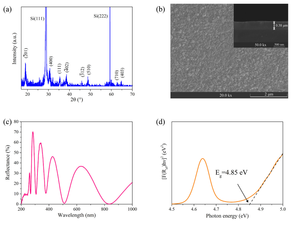
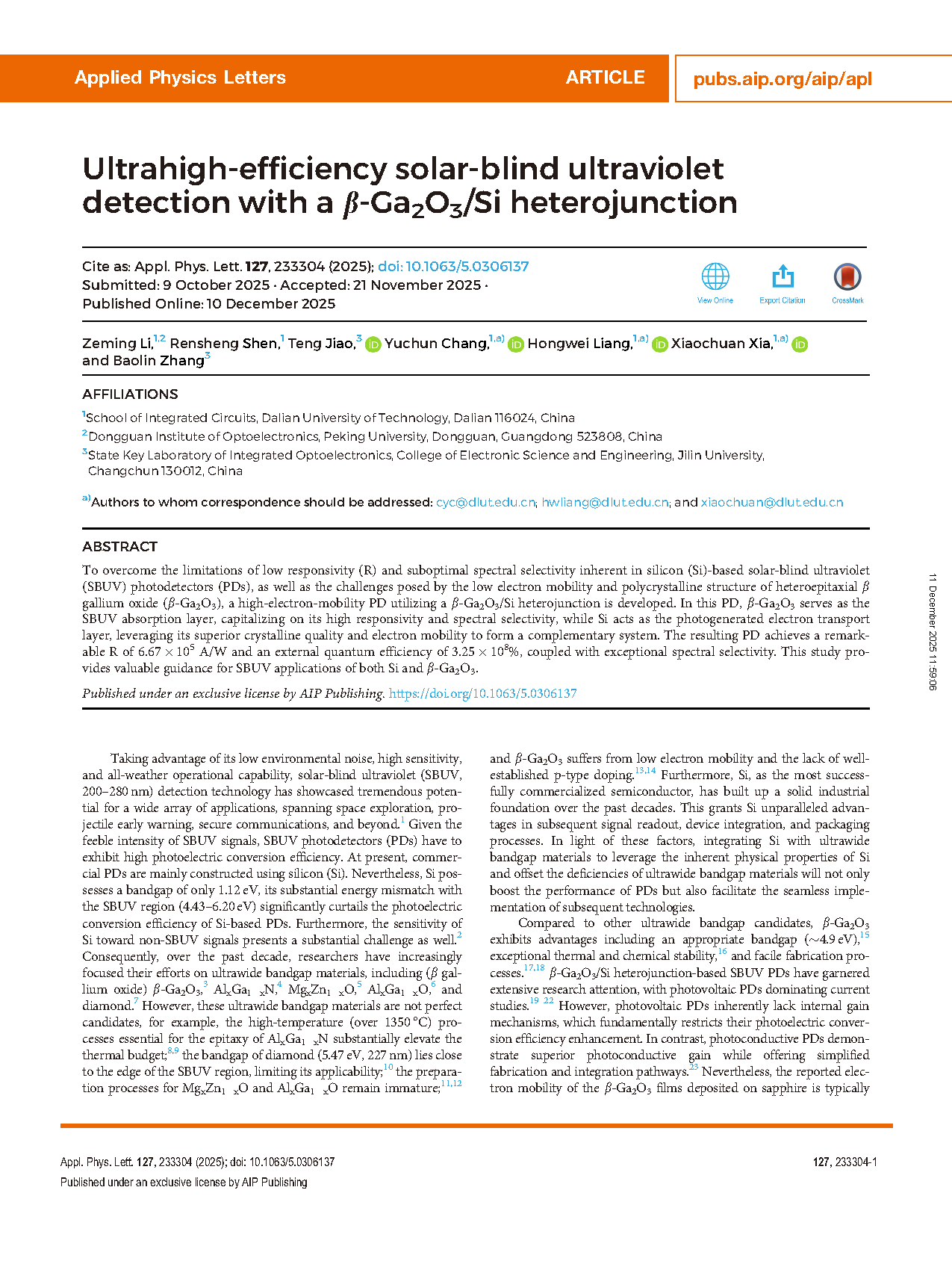
FIG. 1. Characterizations of the deposited sample: (a) XRD pattern; (b) SEM top-view image (inset: cross-sectional view image); (c) reflectance spectrum; (d) bandgap determined by the Kubelka–Munk method. F(Ref)=(1-Ref)2/2Ref, Ref stands for the reflectance.
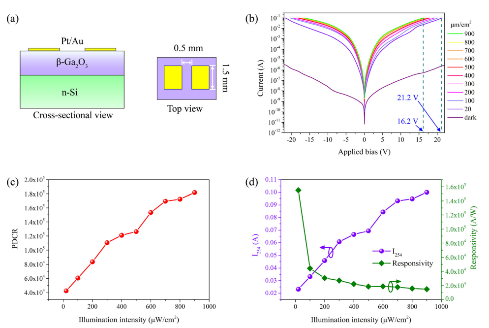
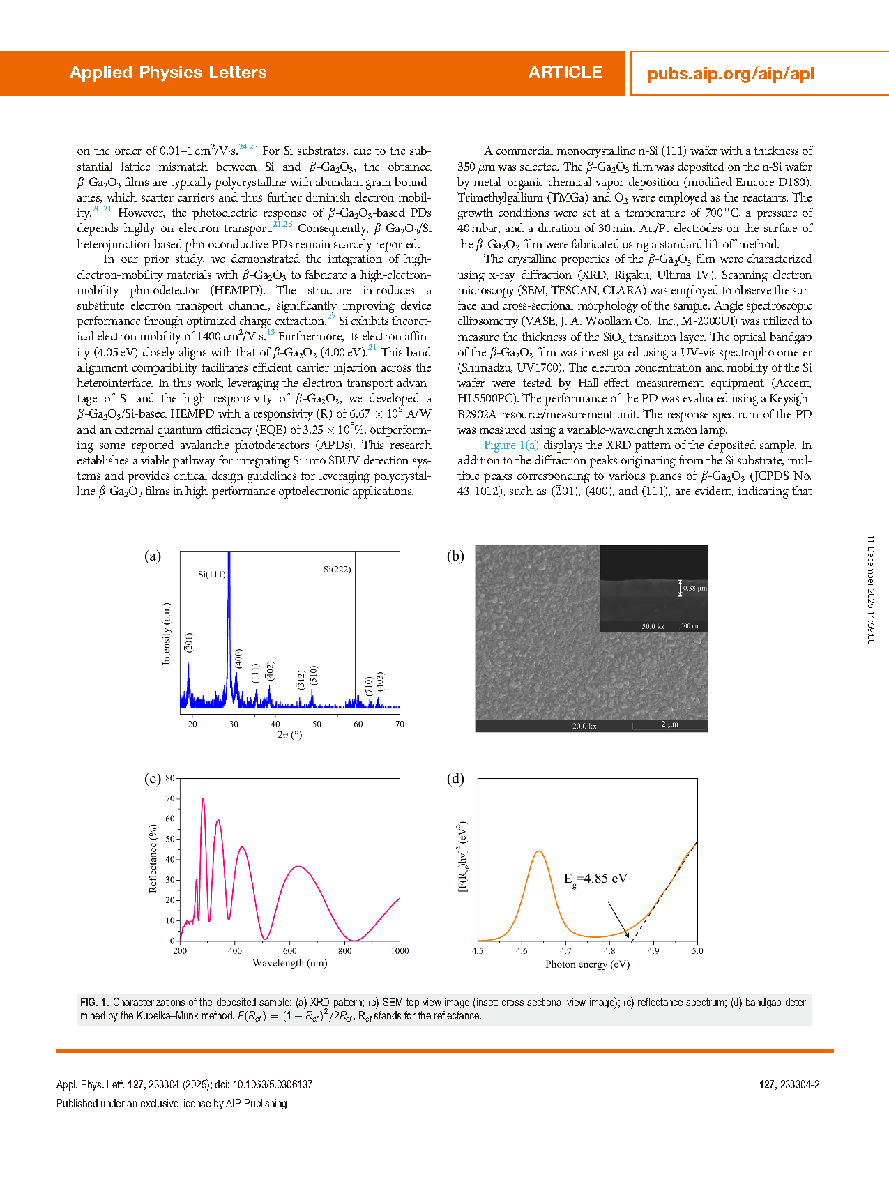
FIG. 2. (a) Schematic diagram of the fabricated PD; the performance of the PD subjected to varying intensities of 254 nm illumination: (b) I–V curves; (c) PDCR at 16.2 V bias; (d) I254 and R at 16.2 V bias.
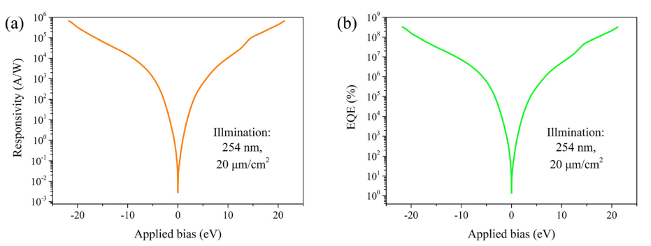
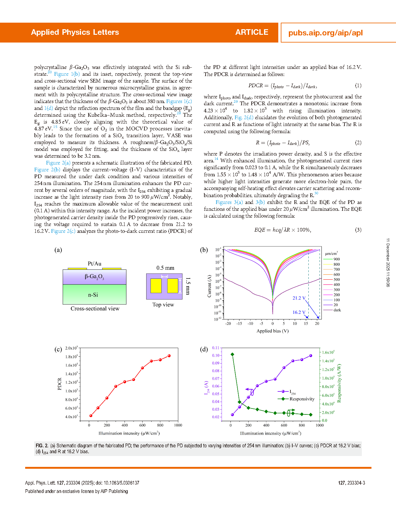
FIG. 3. (a) The R and (b) the EQE of the obtained PD under 254 nm illumination with an intensity of 20 μW/cm2.
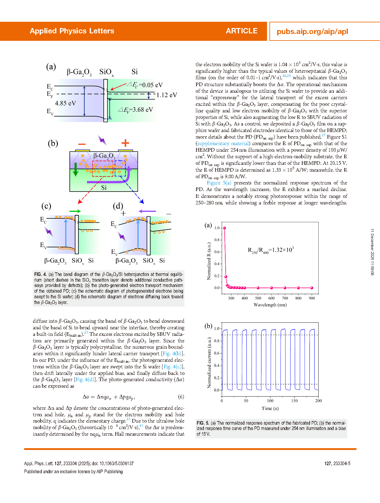
FIG. 4. (a) The band diagram of the β-Ga2O3/Si heterojunction at thermal equilibrium (short dashes in the SiOx transition layer denote additional conductive pathways provided by defects); (b) the photo-generated electron transport mechanism of the obtained PD; (c) the schematic diagram of photogenerated electrons being swept to the Si wafer; (d) the schematic diagram of electrons diffusing back toward the β-Ga2O3 layer.
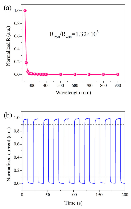
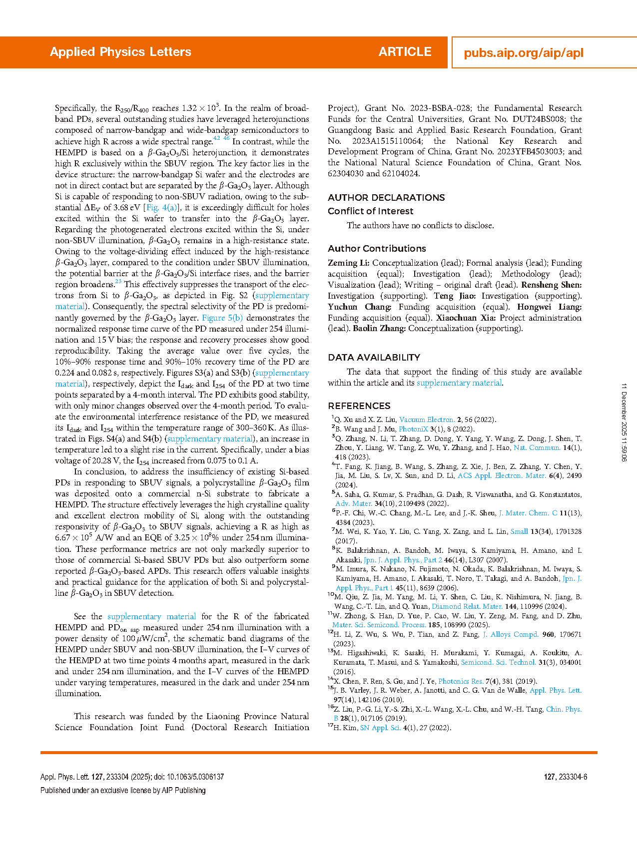
FIG. 5. (a) The normalized response spectrum of the fabricated PD; (b) the normalized response time curve of the PD measured under 254 nm illumination and a bias of 15 V.
DOI:
doi.org/10.1063/5.0306137