


News Trends
【World Express】FLOSFIA Achieves New Progress in the Mass Production of Gallium Oxide Power Semiconductors
日期:2025-12-25阅读:875
FLOSFIA, Inc., a global pioneer in the practical application of Gallium Oxide (α-Ga₂O₃) power semiconductors, has successfully completed the validation of 4-inch wafer manufacturing technology, a key milestone for mass production, and has overcome critical challenges related to product reliability.
Amid intensifying global cost competition and structural challenges facing the Silicon Carbide (SiC) industry, FLOSFIA’s innovative materials technology is positioned as a “game changer,” laying a solid foundation for restoring the competitiveness of Japan’s semiconductor industry.
■ Intense Competition in SiC and Challenges Facing Japan’s Semiconductor Industry
At present, the Silicon Carbide (SiC) market—positioned as a key pillar of next-generation power semiconductors—has fallen into extremely intense cost competition approaching a price collapse, driven by the slowdown in electric vehicle demand and large-scale investments by Chinese manufacturers. Although Japanese companies continue to maintain technological advantages, their competitiveness is rapidly eroding due to structurally high cost structures. As a result, Japan’s semiconductor industry, which once dominated the global market, now faces the severe prospect of a “second failure.”
■ A Historic Opportunity Driven by the Rapid Expansion of the “New Materials Power Semiconductor” Market
With the explosive adoption of generative AI, power demand from data centers is increasing sharply. At the same time, under the imperative of achieving a carbon-neutral society, dramatic improvements in power conversion efficiency have become an urgent priority. The market for power semiconductors based on materials other than silicon (Si) is expected to grow at an exceptional compound annual growth rate (CAGR) of approximately 20% over the next decade, reaching a market size of around 3.5 trillion yen by 2035.
■ A Key Milestone for Mass Production: Addressing Structural Cost Challenges with Original Japanese Technology
FLOSFIA has achieved significant breakthroughs in the development of mass-production critical technologies. The following two technical achievements are highlighted.
Achievement 1: Completion of 4-Inch Wafer Manufacturing Technology Validation
FLOSFIA has successfully achieved its previously announced goal of completing the validation of 4-inch wafer manufacturing technology by 2025. This milestone lays the foundation for establishing a large-scale mass production system and provides a clear path toward achieving a decisive cost advantage. The company’s proprietary technology fundamentally addresses the structural high-cost challenges faced by the SiC industry.
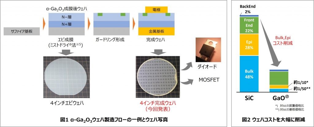
1.Innovative Reduction of Substrate Costs
In SiC device manufacturing, SiC substrates account for approximately half (48%) of the total cost. In contrast, for α-Ga₂O₃ devices, by utilizing widely available and low-cost sapphire substrates, the substrate cost can be reduced to as little as 1/50 of the original.
2.Significant Reduction in Growth Costs
FLOSFIA’s proprietary Mist-DRY® crystallization system can reduce equipment investment to less than 1/10 of that required for conventional SiC crystallization systems (such as MOCVD or HVPE), offering the potential for substantial reductions in crystal growth costs.
3.Efficient Upstream Process Implementation
By collaborating with existing GaN-LED and SiC factories, FLOSFIA can leverage already-invested process equipment and, combined with 4-inch multi-wafer processing, greatly accelerate the preparation for mass production.
With Japan’s advantages in materials technology and process innovation, the previously considered unattainable goal of achieving ultra-low-loss performance surpassing SiC while maintaining costs comparable to silicon (Si) is gradually becoming a reality.
Achievement 2: Overcoming Reliability Issues in Schottky Barrier Diodes (SBDs)
FLOSFIA previously faced reliability deviations caused by surface processing of α-Ga₂O₃. The company has now successfully identified the main causes and established corresponding countermeasure technologies.
By testing using 100 μm microchips, significant improvement in reliability yield was observed, confirming that the primary causes of defects were minor surface irregularities and specific crystal defects. In response, FLOSFIA developed a highly sensitive method to detect minute surface irregularities across the entire wafer and established proprietary crystal defect detection technology, achieving substantial improvements in reliability deviations.
With these countermeasure technologies implemented, FLOSFIA verified significant enhancements in products at the voltage/current rating of 600 V / 10 A, which corresponds to mainstream specifications for both consumer and industrial device applications.
・Significant Reduction in Leakage Current:
Compared with the previous state, the leakage current under applied reverse voltage has been reduced to less than 1/1000.
・Ensuring Long-Term Reliability in Harsh Environments:
Under accelerated testing with continuous reverse bias at 150 °C, no breakdown was observed even after 1,500 hours.
・Improved Yield Enhancing Mass Production:
By substantially reducing reliability fluctuations, mass-production yield is improved, further strengthening cost competitiveness.
The established reliability countermeasure technologies provide clear guidance for meeting market-required reliability standards. Furthermore, these technologies are not limited to SBDs; they can also be applied to future product lines, including JBS diodes and MOSFETs. Leveraging this common foundational technology will accelerate the overall launch of early product lines.
■ Future Outlook: Pioneering the “Post-SiC” Era with Original Japanese Technology
Building on these achievements, FLOSFIA will accelerate the establishment of mass-production technologies for MOSFETs, targeting over 70% market share, and JBS diodes as the next-generation diode. The experience gained from yield improvement and process optimization in the early mass-production development of SBDs will serve as a key advantage for enabling the early market introduction of these flagship products.
■ Strengthening the Competitiveness of Japan’s Semiconductor Industry
For Japan’s SiC industry, which is at a disadvantage in global cost competition, FLOSFIA’s α-Ga₂O₃ technology offers the following advantages:
・Performance: Ultra-low-loss characteristics surpassing those of SiC
・Cost: Manufacturing costs comparable to silicon (Si)
・Technological Uniqueness: Centered on Japan’s strengths in materials technology
・Intellectual Property Protection: High entry barriers established through proprietary technology
At the same time, the company is actively promoting the establishment of global partnerships through intellectual property licensing and the supply of epitaxial wafers, aiming to achieve mass production by 2026.
Under its “Semiconductor Ecosystem®” concept, FLOSFIA is committed to reducing waste across three key areas—energy loss, process loss, and material loss—contributing to a sustainable society and alleviating the environmental burden on the planet.
