Paper Sharing
【Domestic Papers】Investigation of dislocation mobility on the cast-grown β-Ga₂O₃:(100) by nanoindentation
日期:2025-12-25阅读:489
Researchers from the Zhejiang University have published a dissertation titled "Investigation of dislocation mobility on the cast-grown β-Ga2O3:(100) by nanoindentation" in Journal of Alloys and Compounds.
Project Support
This work was supported by the National Key Research and Development Program of China (2024YFE0205300), “Pioneer” and “Leading Goose” R&D Program of Zhejiang (2023C01193), the National Natural Science Foundation of China (22205203), the Natural Science Foundation of Zhejiang (LZ25E070001), the National Program for Support of Topnotch Young Professionals, and the Leading Innovative and Entrepreneur Team Introduction Program of Hangzhou (TD2022012).
Background
Beta-phase gallium oxide (β-Ga2O3) has garnered significant attention as an ultra-wide bandgap semiconductor due to its remarkable intrinsic properties including an ultra-wide bandgap (∼4.8 eV), a high critical breakdown field (∼8 MV/cm), an outstanding Baliga figure of merit (BFOM) exceeding 3200, and an optical absorption edge near 260 nm. These attributes provide notable advantages over other wide bandgap semiconductors such as SiC and GaN, making β-Ga2O3 a promising candidate for applications in power electronic and optoelectronic devices. Recently, 6–8 in. β-Ga2O3 single ingots have been successfully obtained through melt-growth methods. Owing to its high thermodynamically stability and lower surface energy, the (100) plane became the principal plane in EFG and casting methods, which has advantages in crystal size amplification and commercialization. To date, numerous investigations have focused on crystal growth defects doping optoelectronic characteristics and devices fabrication. However, due to its monoclinic structure with lattice constants of a = 12.2 Å, b = 3.0 Å, c = 5.8 Å, and β = 103.7˚, the typical low-symmetry structure endows strong anisotropy, also reflected in the anisotropy mechanical properties, which demands further comprehensive investigation.
Abstract
A deeper comprehension of dislocation dynamics in β-Ga2O3 is critical for optimizing crystal growth and enhancing device performance. In this study, dislocation mobility in (100) substrates at room temperature and elevated temperatures was systematically investigated via nanoindentation, wet chemical etching, rapid thermal processing, confocal laser scanning microscope, X-ray topography and transmission electron microscopy. The results demonstrate that dislocations propagate along the < 010 > / {001} slip system, with an activation energy of 0.801 eV. Notably, we unveil that dislocations in β-Ga2O3 exhibit room-temperature mobility, with glide length strongly dependent on the applied peak load. Furthermore, this work provides the experimental evidence for dislocation dynamics and establishes a quantitative model for predicting dislocation motion under various load and annealing temperature. The insights gained from this work offer valuable guidance for engineering defect-controlled surfaces to enable high-performance β-Ga2O3-based power electronic devices.
Highlights
● Visualization of β-Ga2O3 Dislocation Gliding: The study achieves the visualization of dislocation slip paths by wet chemical etching in β-Ga2O3, thereby simplifying the research methods and improving efficiency.
● Comprehensive understanding on β-Ga2O3 Dislocation Dynamics: The article studies the dislocation mobility within the (100)-orientation samples at room temperature and elevated temperatures, which provides the experimental evidence for dislocation dynamics and offers a reliable prediction formula for dislocation gliding.
● Technological Significance: The findings provide new approach for the research on the mechanical properties of β-Ga2O3, that is, to understand the mechanical properties of crystals by the ability of dislocation gliding.
Conclusions
In conclusion, an efficient method has been developed to evaluate the load and temperature dependence of dislocation gliding length. Nanoindentation tests were conducted to induce dislocation rosettes on the β-Ga2O3:(100) plane. Through TEM characterization, dislocations were revealed propagating in the < 010 > / {001} slip system along the [010] direction, which was further supported in XRT measurements. CLSM combined with chemical etching was employed to estimate the dislocation velocity and the activation energy of the dislocation mobility under various load and temperature conditions. Finally, an activation energy of 0.801 eV for dislocations in β-Ga2O3 was obtained precisely determined via RTP experiments, which is akin to GaN and ZnO but significantly lower than that of silicon, 4H-SiC and ZrO2, aligning with the experimental observations. These findings provide valuable insights into dislocation dynamics and may be instrumental in predicting the effects of loading during wafer processing and/or device fabrication on dislocation generation and multiplication in β-Ga2O3.
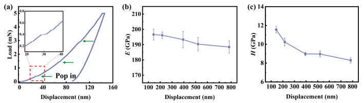
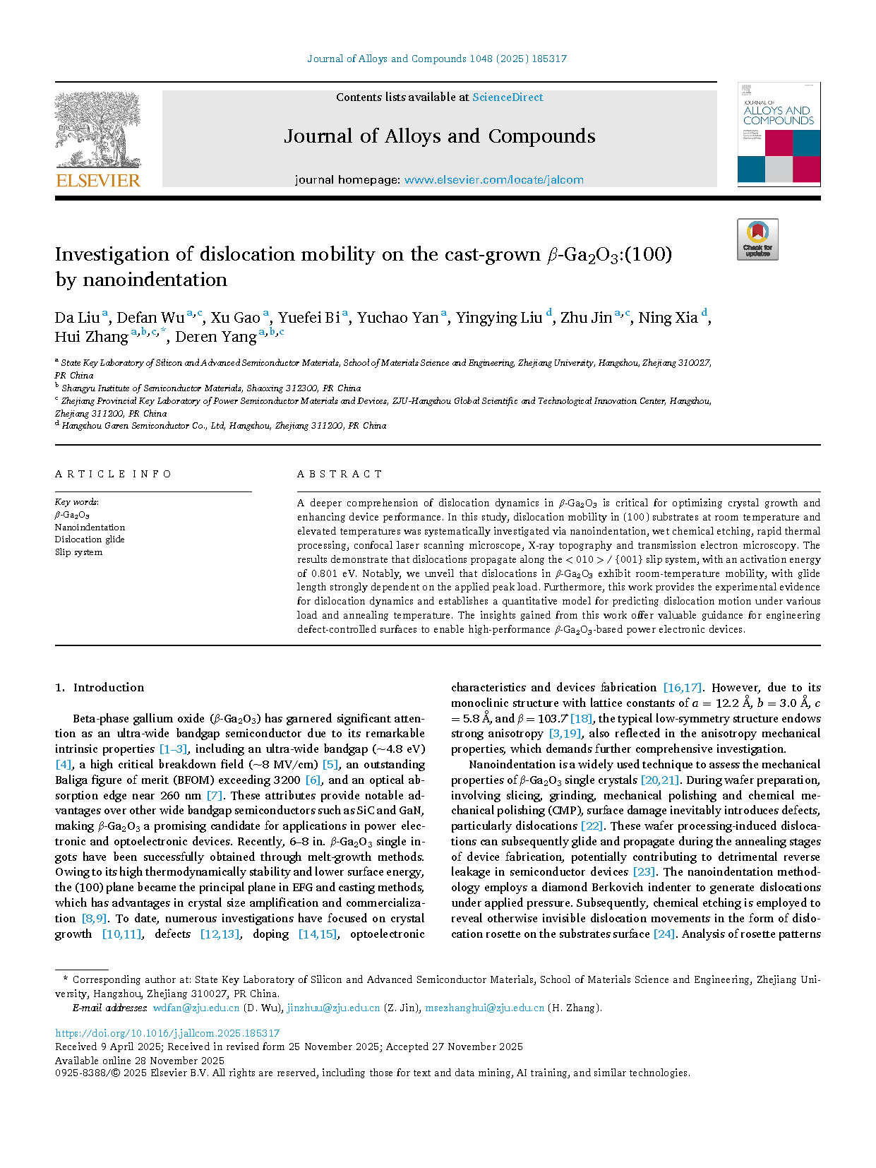
Fig. 1. (a) The P-h curve with the peak load of 5 mN, (b) Young’s modulus (E) and (c) Hardness (H) as a function of displacement.
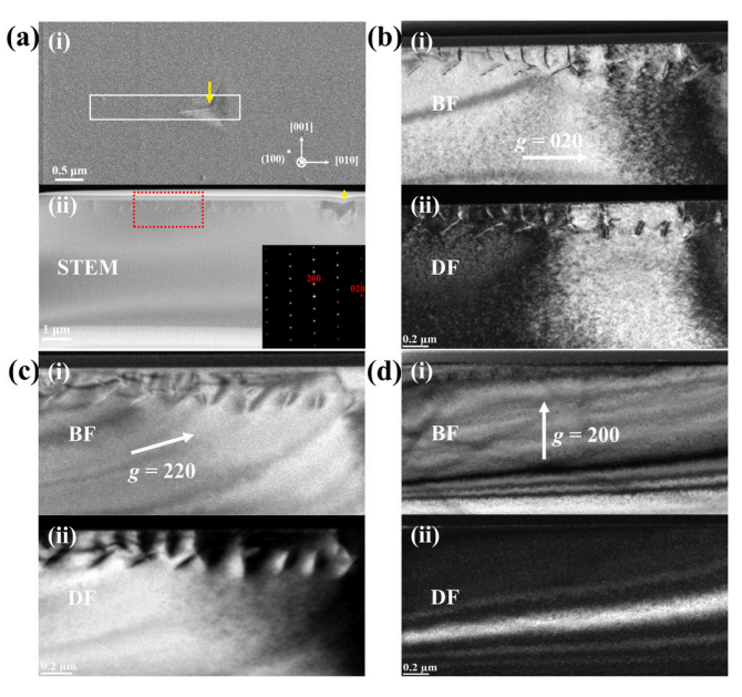
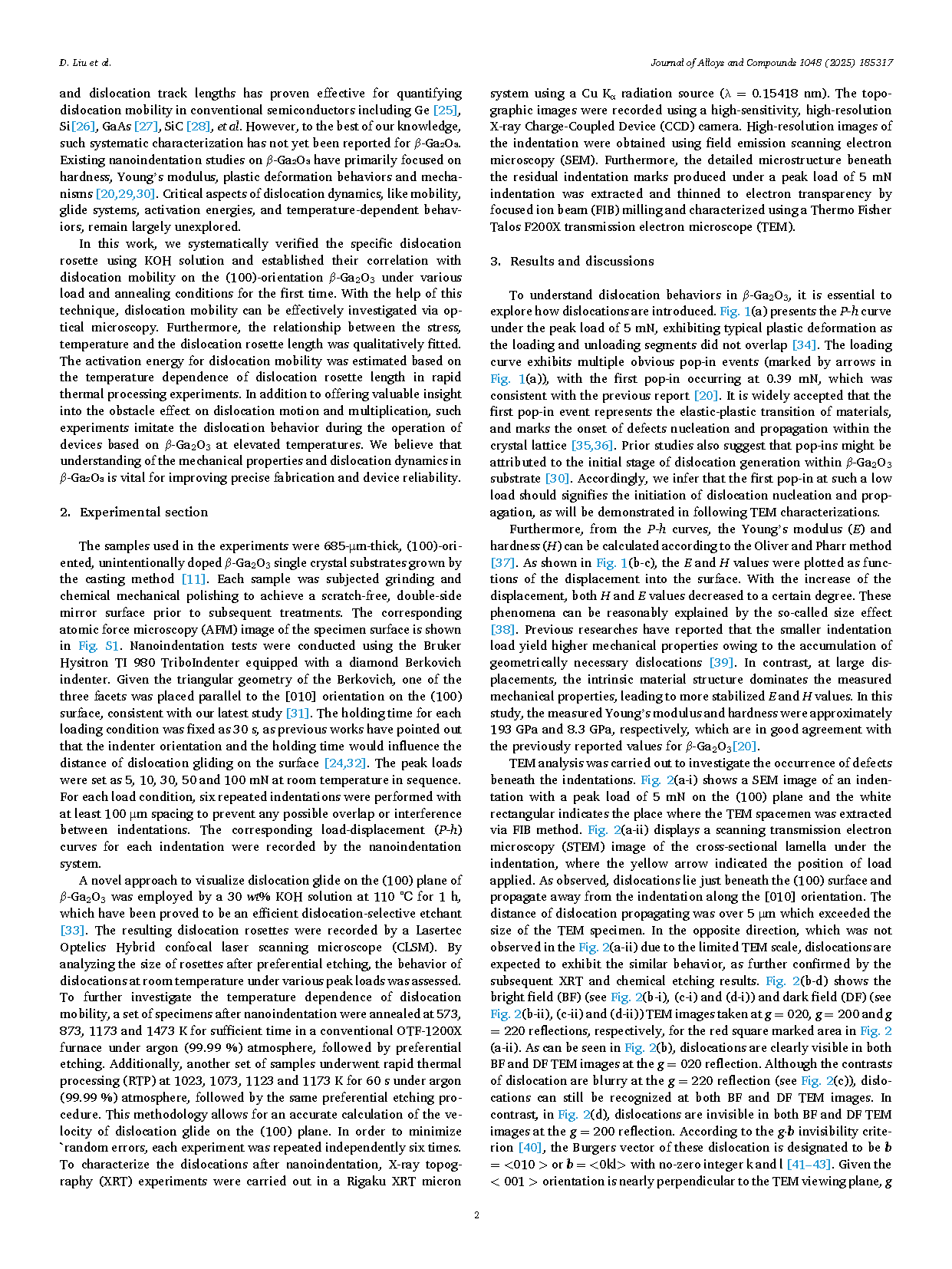
Fig. 2. (a-i) A SEM image of an indentation with a peak load of 5 mN on the (100) plane and the white rectangular indicates the place where the TEM spacemen was extracted via FIB method. (a-ii) A STEM image of the cross-sectional lamella under the indenter. (b-i) BF and (b-ii) DF TEM images taken at g = 020 reflection, (c-i) BF and (c-ii) DF TEM images taken at g = 220 reflection, and (d-i) BF and (d-ii) DF TEM images taken at g = 200 reflection for the red square marked area in (a-ii).
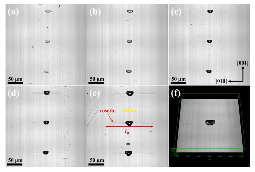
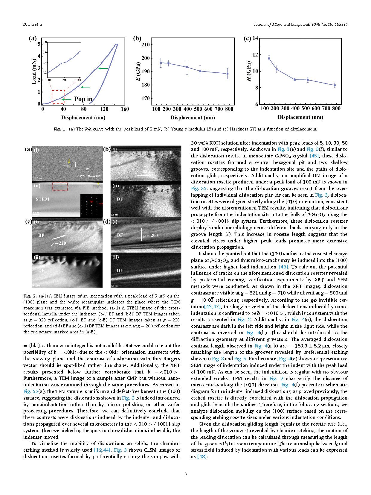
Fig. 3. The CLSM images of the dislocation rosettes induced by the indent with the peak load of (a) 5 mN, (b) 10 mN, (c) 30 mN, (d) 50 mN and (e) 100 mN. (f) Three-dimensional image of a representative rosette shown in (e).
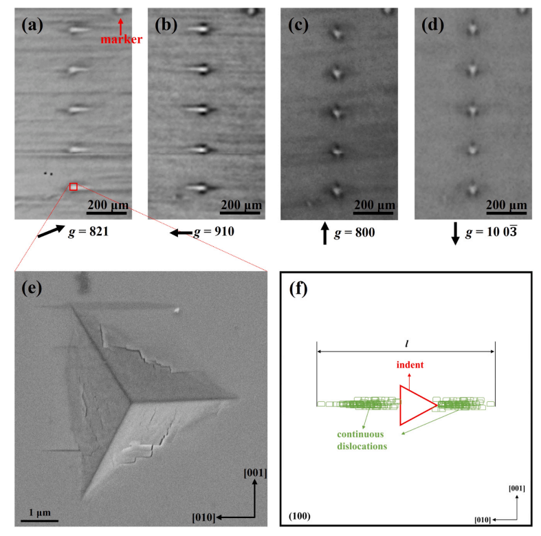
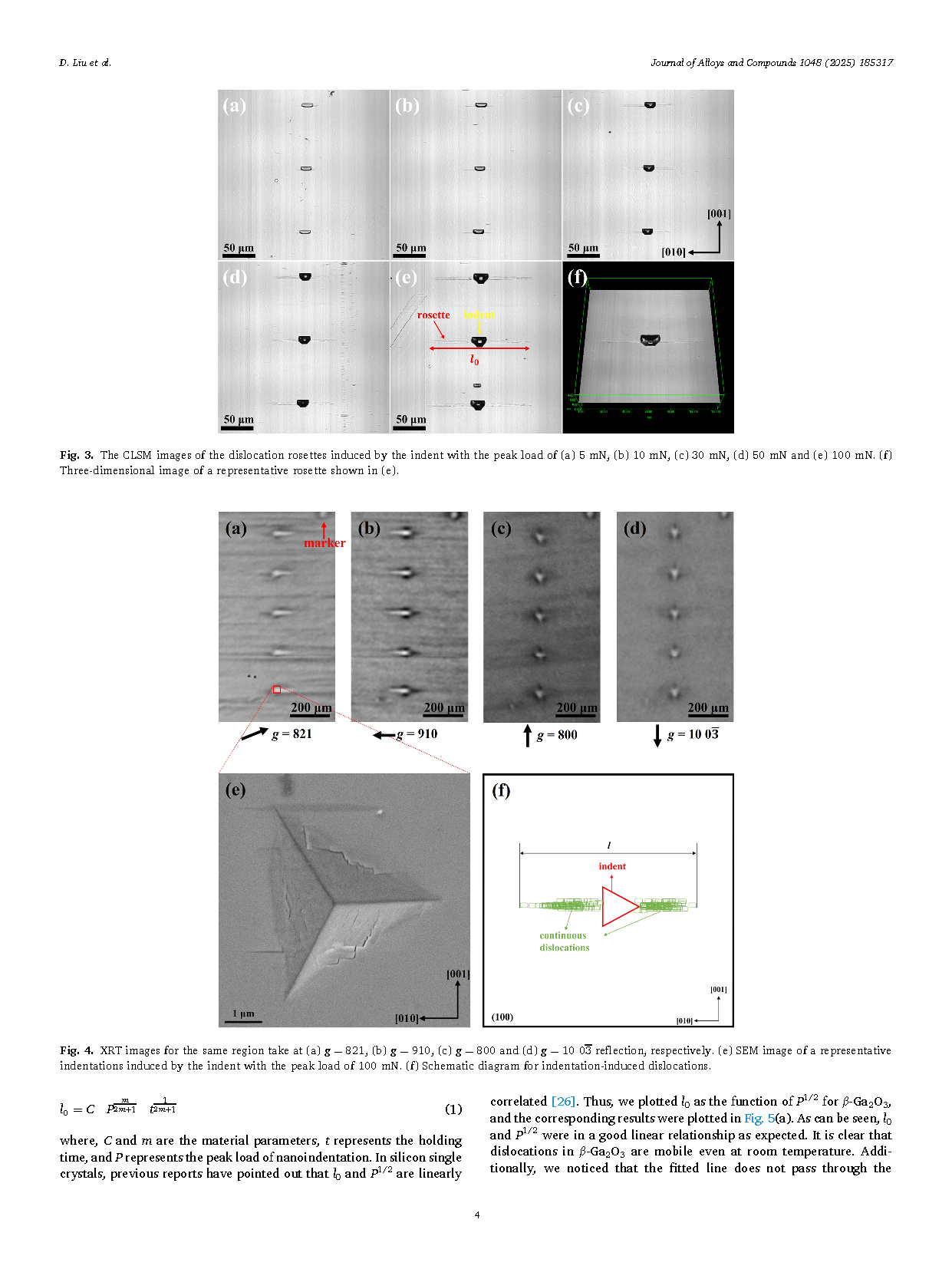
Fig. 4. XRT images for the same region take at (a) g = 821, (b) g = 910, (c) g = 800 and (d) g = 10 03 reflection, respectively. (e) SEM image of a representative indentations induced by the indent with the peak load of 100 mN. (f) Schematic diagram for indentation-induced dislocations.
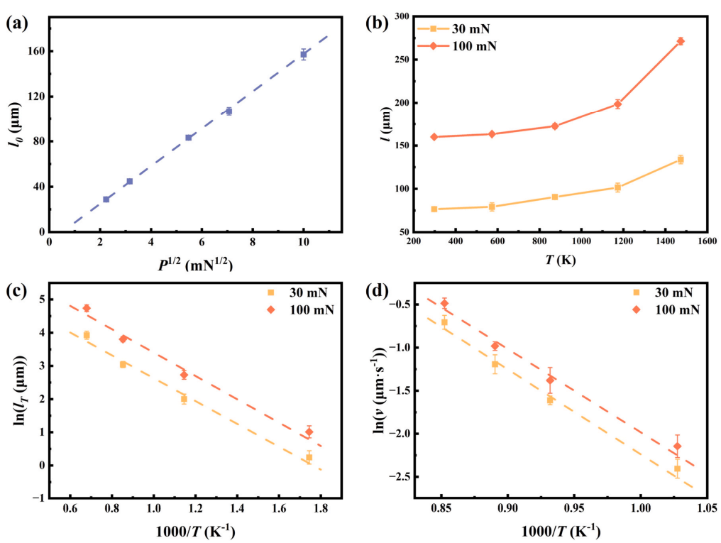
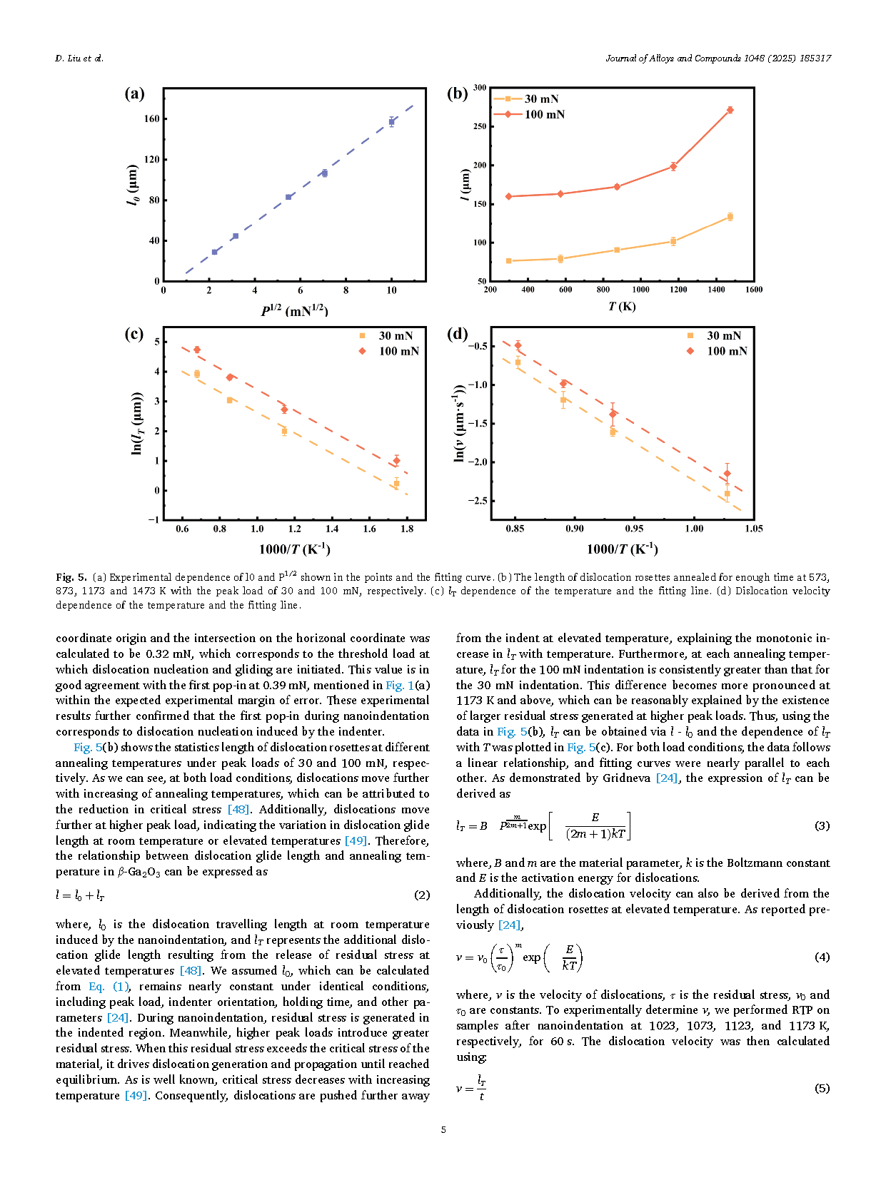
Fig. 5. (a) Experimental dependence of l0 and P1/2 shown in the points and the fitting curve. (b) The length of dislocation rosettes annealed for enough time at 573, 873, 1173 and 1473 K with the peak load of 30 and 100 mN, respectively. (c) lT dependence of the temperature and the fitting line. (d) Dislocation velocity dependence of the temperature and the fitting line.
DOI:
doi.org/10.1016/j.jallcom.2025.185317