Paper Sharing
【Member Papers】Boosting Performance of Ga₂O₃ Thin-Film Transistors via Defect Passivation toward Solar-Blind Ultraviolet In-Sensor Reservoir Computing
日期:2025-12-29阅读:527
Researchers from the Northeast Normal University have published a dissertation titled "Boosting Performance of Ga2O3 Thin-Film Transistors via Defect Passivation toward Solar-Blind Ultraviolet In-Sensor Reservoir Computing" in ACS Nano.
Project Support
This work was supported by the National Key Research and Development Program (2021YFA0716404, 2024YFA1208800), the NSFC Program (Nos. U23A20568, 12474164, 52372137, 62571109), the 111 Project (No. B25030), the funding from Jilin Province (No. 20240101129JC), and the Scientific Research Innovation Capability Support Project for Young Faculty (Grant No. ZYGXQNJSKYCXNLZCXM-I10).
Background
Wide-bandgap metal-oxide semiconductor thin-film transistors (TFTs) have crucial applications in displays, sensors, and memorizers. Conventional metal-oxide semiconductors such as ZnO, In2O3, and SnO2 and their alloys with Ga2O3, which exhibit high visible-light transparency and adjustable electron concentrations, are widely employed as channel materials in contemporary TFTs. Typically, amorphous indium gallium zinc oxide (IGZO) TFTs have been commercialized as pixel TFT backplanes in high-resolution organic light-emitting displays. However, their relatively narrow bandgap of approximately 3.6 eV and existing deep-level defects render IGZO TFTs less stable under high temperatures, bias stress, or solar light irradiation. Consequently, there is increasing interest in exploring ultrawide bandgap metal-oxide semiconductors to enhance TFT device performance and extend their application beyond traditional fields.
Abstract
Ga2O3 thin-film transistors (TFTs) are resilient to high temperatures and voltages and are suitable for demanding display and sensing applications. Nevertheless, the performance of current Ga2O3 TFTs is constrained by defect-induced impediments to free carrier transport. This work introduces a strategy comprising nitrogen annealing followed by Al2O3 encapsulation via atomic layer deposition, which boosts the mobility and solar-blind UV responsivity of Ga2O3 TFTs by more than 27-fold and 94-fold, respectively. The combined results of high-resolution transmission electron microscopy characterization and computer-aided design simulation ascribe these enhancements to the effective passivation of deep-level defects at the interface, in the bulk, and on the surface of Ga2O3. Furthermore, the competition and synergy between photoconduction and gating in Ga2O3 TFTs yield a gate-voltage-programmable photoresponse, allowing for the control of both the responsivity and response time. Leveraging this, a solar-blind UV in-sensor reservoir computing system based on Ga2O3 TFTs is demonstrated, which achieves over 91.8% accuracy in fingerprint image recognition even under 40% noise. This work integrates an effective defect passivation strategy with a clarified modulation mechanism and further demonstrates its application in neuromorphic computing. The approach presented here shows a broad potential for extension to other wide-bandgap semiconductor systems.
Conclusion
In summary, we have developed a strategy that combines high-temperature nitrogen annealing with an Al2O3 capping layer to enhance the electrical and photodetection performance of Ga2O3 TFTs. This treatment passivates the deep-level defects and surface states in Ga2O3 TFTs, leading to improvements in mobility, on−off current ratio, and stability. The optimized Ga2O3 TFTs exhibit a photo-to-dark current ratio of up to 105, a detectivity of 7.6 × 10¹⁴ Jones, and rapid decay times of 0.3 s under solar-blind UV illumination. Current density simulation and HRTEM characterization corroborate that nitrogen annealing reduces the transit time of photogenerated carriers, while the Al2O3 capping layer effectively suppresses surface carrier depletion, thereby enhancing the photodetection capabilities of Ga2O3 TFTs. We have clarified the synergistic and competitive relationships between the photoconduction and gating mechanisms within Ga2O3 TFTs, which empower these gate-voltage-programmable devices to act as optoelectronic synapses for RC and high-precision fingerprint image recognition applications. The insights obtained regarding defect passivation and its impact on the optoelectronic characteristics of Ga2O3 TFTs not only advance the development of neuromorphic visual systems but also provide valuable guidance for the advancement of other metal-oxide-semiconductor technologies.
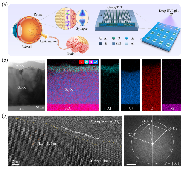
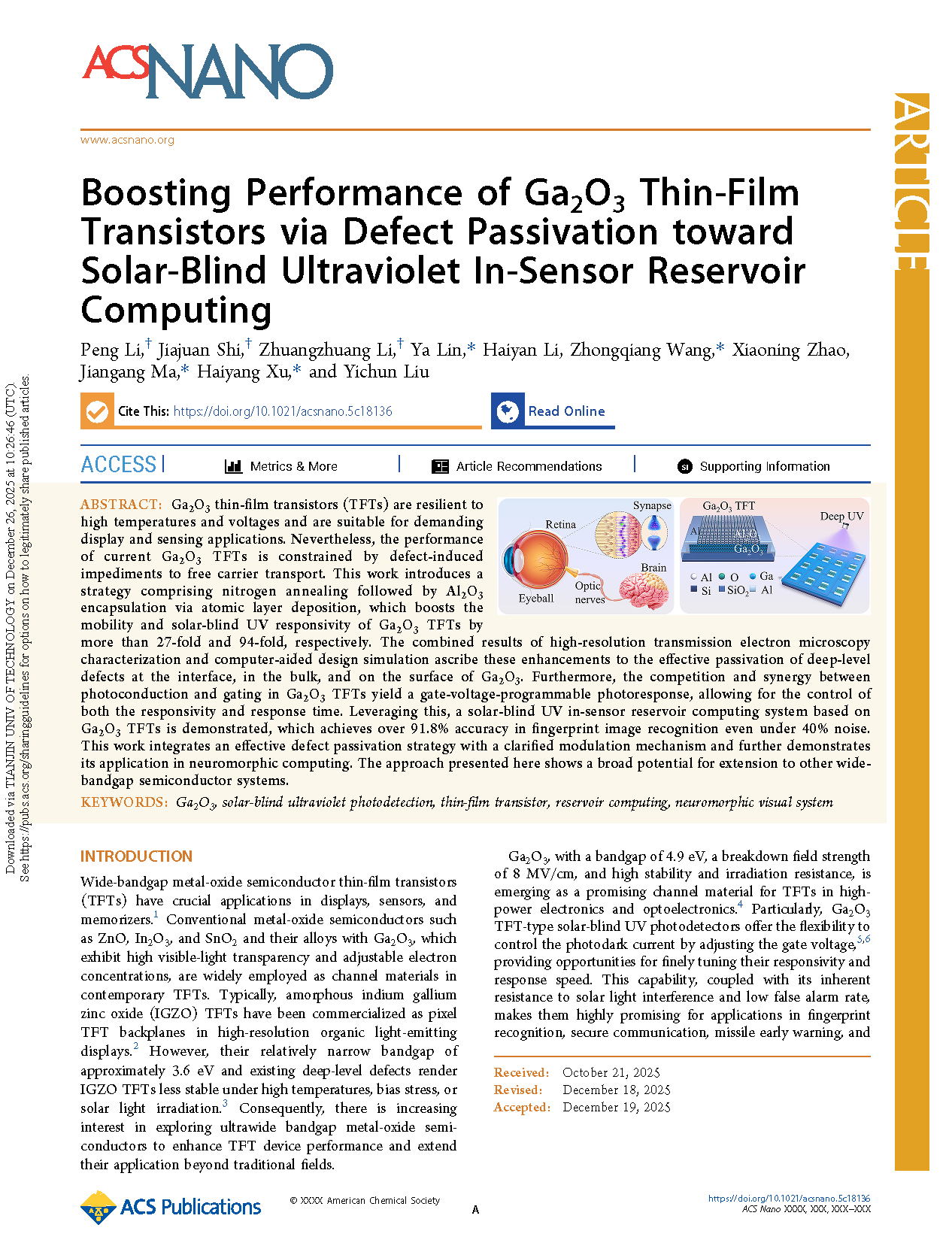
Figure 1. Ga2O3 TFTs for neuromorphic visual systems. (a) Illustration of the schematic for the biological visual system and a neuromorphic visual system designed by using a Ga2O3 TFT array. (b) HAADF-STEM image and corresponding energy-dispersive spectroscopy mapping of the elements Al, Ga, O, and Si in the Ga2O3/Al2O3 heterojunction film deposited on a SiO2/Si substrate. (c) High-resolution TEM image of the Ga2O3/Al2O3 heterojunction, showing the amorphous Al2O3 layer on the crystalline β-Ga2O3 surface. The corresponding fast Fourier transform pattern (zone axis Z = [101]) displays a diffuse halo from the amorphous Al2O3 and discrete diffraction spots from the (20−2), (11−1), and (1−11) planes of β-Ga22O3.
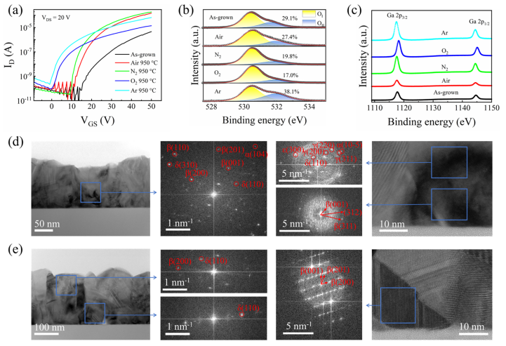
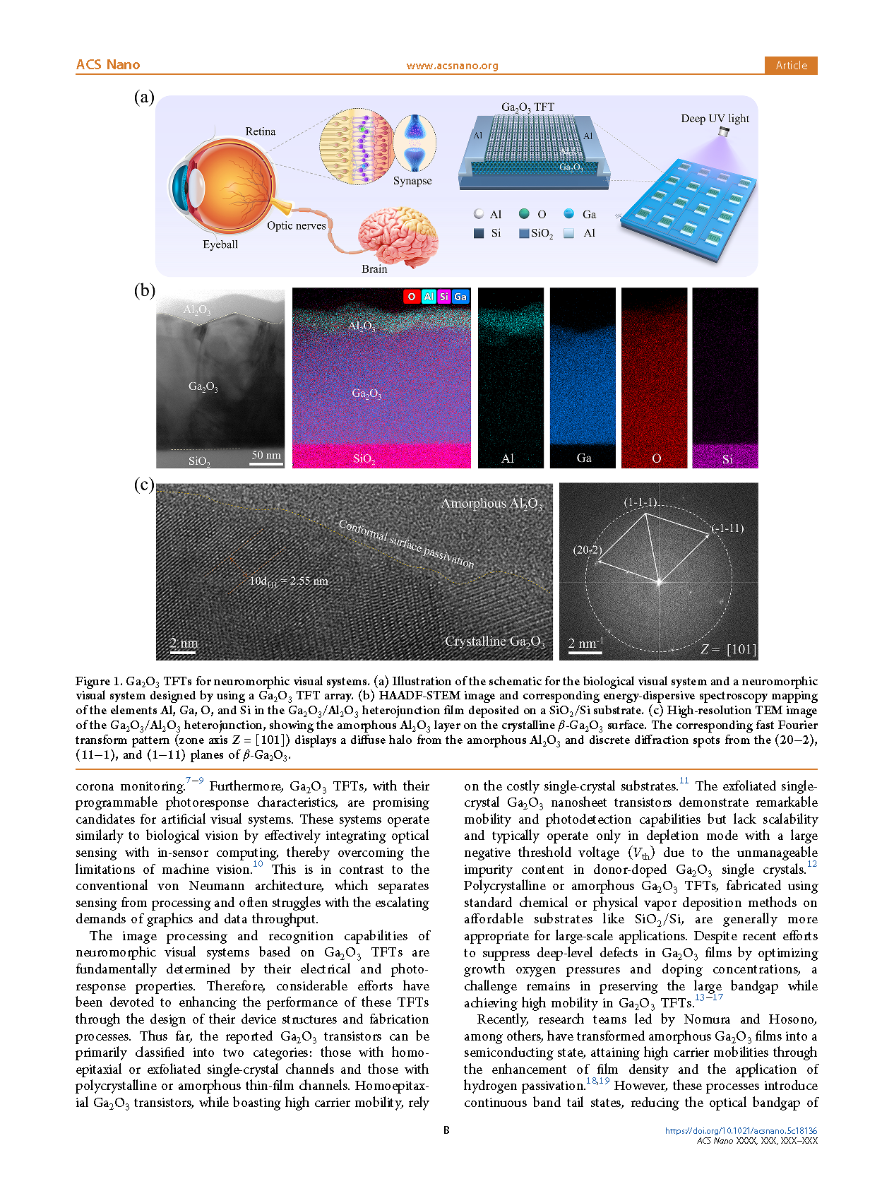
Figure 2. Electrical property enhancement in Ga2O3 TFTs. (a) Transfer characteristic curves of Ga2O3 TFTs before and after annealing under various atmospheres. (b) O 2p and (c) Ga 2p3/2 XPS spectra of Ga2O3 films subjected to annealing in different atmospheres. HAADFSTEM images of the (d) as-grown and (e) annealed Ga2O3 films, accompanied by their respective FFT diffraction patterns from the low- and high-magnification areas.
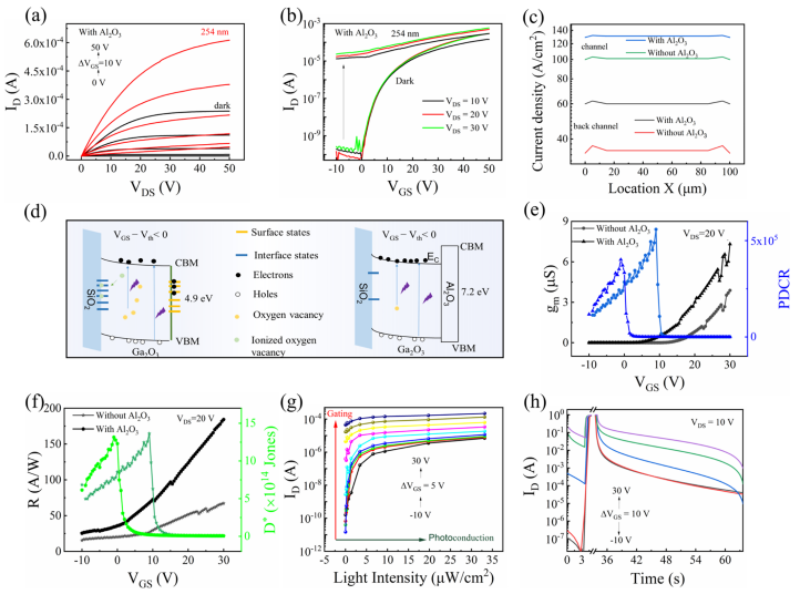
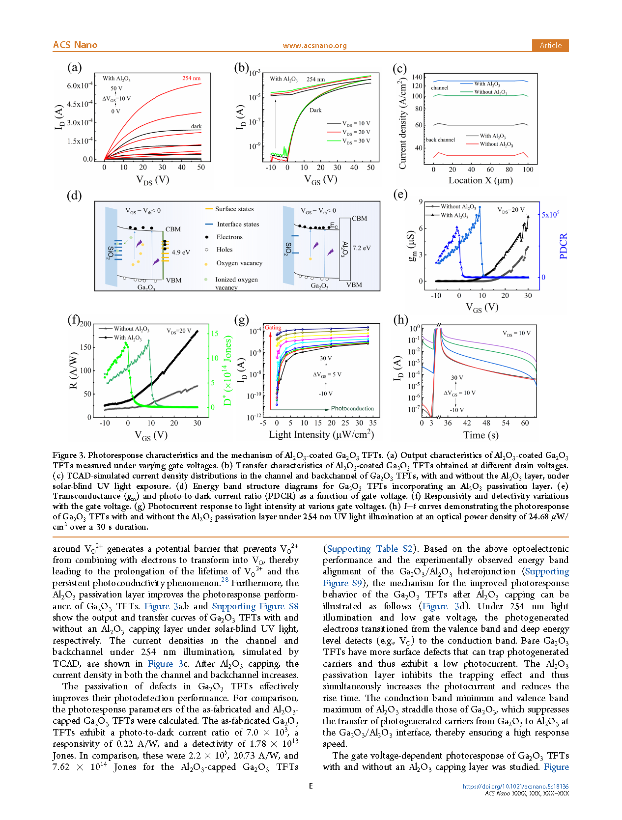
Figure 3. Photoresponse characteristics and the mechanism of Al2O3-coated Ga2O3 TFTs. (a) Output characteristics of Al2O3-coated Ga2O3 TFTs measured under varying gate voltages. (b) Transfer characteristics of Al2O3-coated Ga2O3 TFTs obtained at different drain voltages. (c) TCAD-simulated current density distributions in the channel and backchannel of Ga2O3 TFTs, with and without the Al2O3 layer, under solar-blind UV light exposure. (d) Energy band structure diagrams for Ga2O3 TFTs incorporating an Al2O3 passivation layer. (e) Transconductance (gm) and photo-to-dark current ratio (PDCR) as a function of gate voltage. (f) Responsivity and detectivity variations with the gate voltage. (g) Photocurrent response to light intensity at various gate voltages. (h) I−t curves demonstrating the photoresponse of Ga2O3 TFTs with and without the Al2O3 passivation layer under 254 nm UV light illumination at an optical power density of 24.68 μW/ cm2 over a 30 s duration.
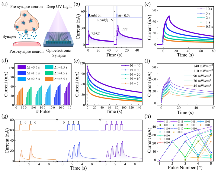
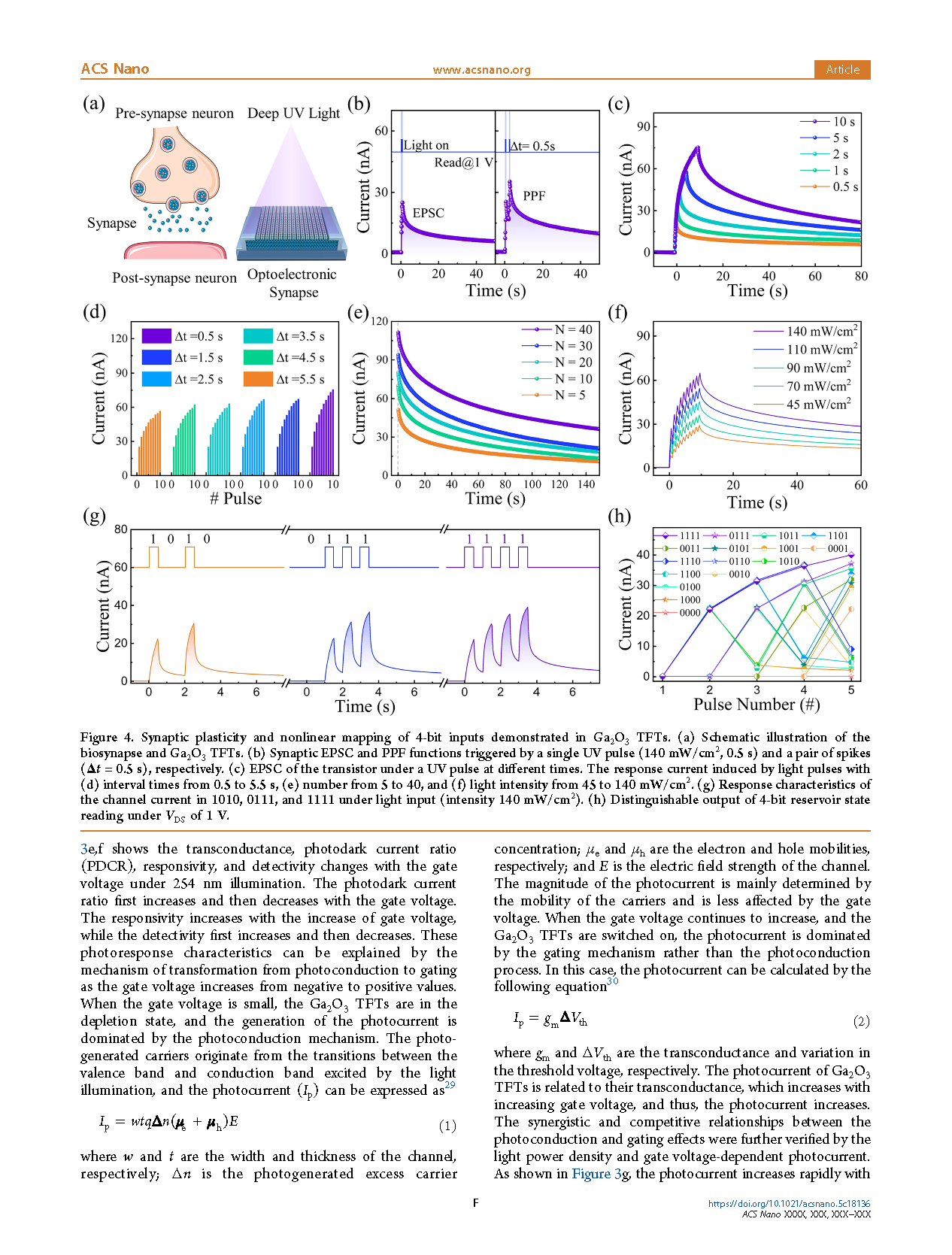
Figure 4. Synaptic plasticity and nonlinear mapping of 4-bit inputs demonstrated in Ga2O3 TFTs. (a) Schematic illustration of the biosynapse and Ga2O3 TFTs. (b) Synaptic EPSC and PPF functions triggered by a single UV pulse (140 mW/cm2, 0.5 s) and a pair of spikes (Δt = 0.5 s), respectively. (c) EPSC of the transistor under a UV pulse at different times. The response current induced by light pulses with (d) interval times from 0.5 to 5.5 s, (e) number from 5 to 40, and (f) light intensity from 45 to 140 mW/cm2. (g) Response characteristics of the channel current in 1010, 0111, and 1111 under light input (intensity 140 mW/cm2). (h) Distinguishable output of 4-bit reservoir state reading under VDS of 1 V.
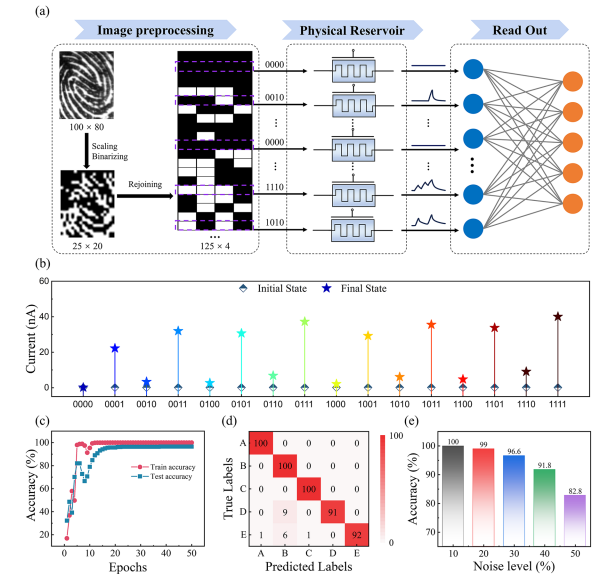
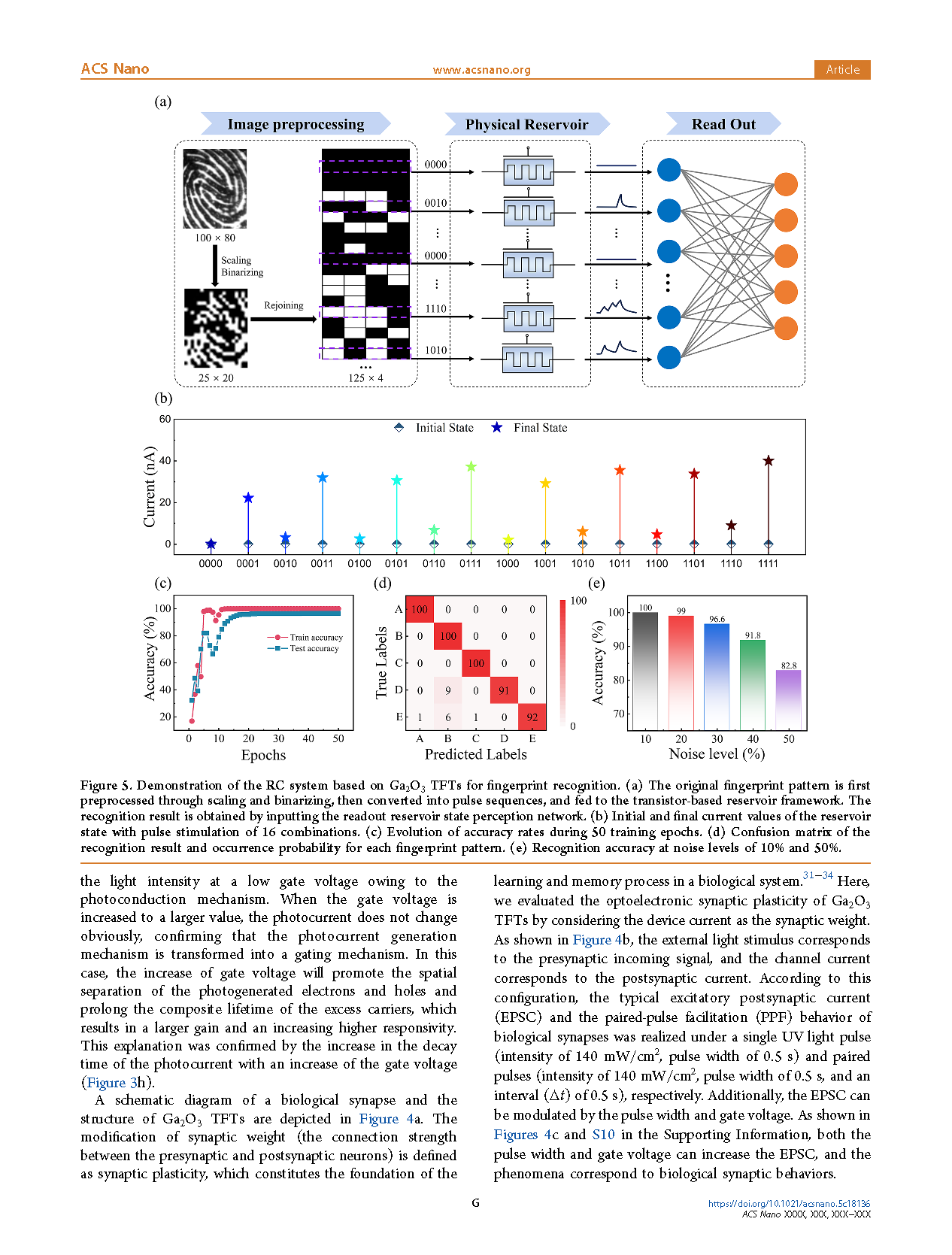
Figure 5. Demonstration of the RC system based on Ga2O3 TFTs for fingerprint recognition. (a) The original fingerprint pattern is first preprocessed through scaling and binarizing, then converted into pulse sequences, and fed to the transistor-based reservoir framework. The recognition result is obtained by inputting the readout reservoir state perception network. (b) Initial and final current values of the reservoir state with pulse stimulation of 16 combinations. (c) Evolution of accuracy rates during 50 training epochs. (d) Confusion matrix of the recognition result and occurrence probability for each fingerprint pattern. (e) Recognition accuracy at noise levels of 10% and 50%.
DOI:
doi.org/10.1021/acsnano.5c18136