


Member News
【Member News】Garen Semiconductor Successfully Grows 8-lnch Gallium Oxide Single Crystal via VB Method
日期:2025-12-31阅读:750
In December 2025, Hangzhou Garen Semiconductor Co., Ltd. (“Garen Semiconductor”) successfully achieved the growth of 8-inch Gallium Oxide (Ga₂O₃) single crystals using the Vertical Bridgman (VB) method, with an 8-inch equivalent diameter length reaching up to 20 mm. This milestone not only marked a perfect conclusion to the company’s 2025 work but also demonstrated its core competitiveness in the Ga₂O₃ field. As the world’s first enterprise to realize multi-technology-route, multi-crystal-plane 8-inch Ga₂O₃ single-crystal production, Garen Semiconductor has established itself as a global leader in Ga₂O₃ materials through a series of original technological breakthroughs.
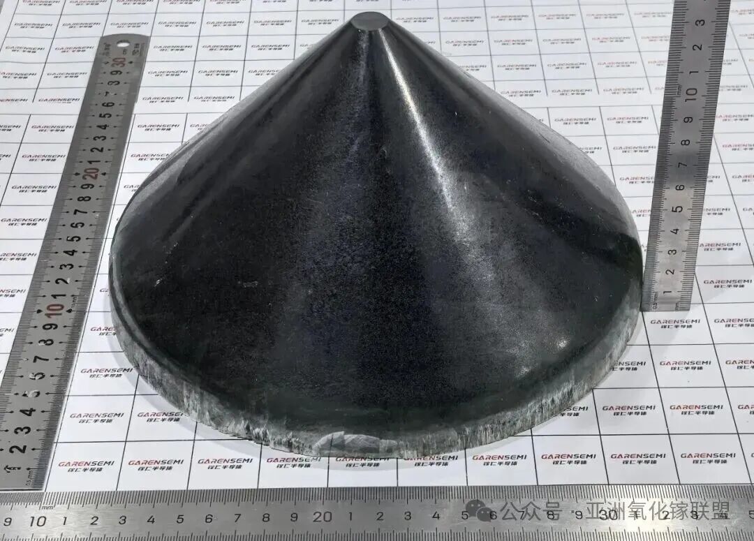
Figure 1 GAREN SEMI VB Method 8-inch Gallium Oxide Bulk
2025 Annual Review
2025.01
Garen Semiconductor successfully grew 4-inch Gallium Oxide single crystals using the Vertical Bridgman (VB) method, marking the first domestic breakthrough of this technology.
2025.03
Using its completely independently developed Casting Method, Garen Semiconductor successfully achieved the world’s first growth of an 8-inch fourth-generation semiconductor Gallium Oxide single crystal, and processed corresponding wafer substrates.
2025.06
Garen Semiconductor used the VB method to prepare 100-mm (010) Gallium Oxide wafer substrates, representing an international first; in the same month, the company also achieved new breakthroughs in Gallium Oxide crystal growth and processing technology, successfully preparing wafer-scale 6-inch slanted Gallium Oxide substrates.
2025.09
Garen Semiconductor’s 8-inch Gallium Oxide substrates passed inspection by both Shenzhen Pinghu Laboratory and Malvern Panalytical Asia-Pacific Application Center, fully confirming the excellent quality of the 8-inch wafers.
2025.10
Garen Semiconductor successfully grew 6-inch (010) Gallium Oxide crystals using the VB method, with equivalent-diameter lengths exceeding 40 mm, reaching international leading levels; in the same month, the company also achieved high-quality 6-inch Gallium Oxide homoepitaxial growth.
2025.11
Relying on its deep technical accumulation, Garen Semiconductor officially launched new (011) plane Gallium Oxide wafer substrates, providing a novel solution for power device fabrication.
2025.12
Garen Semiconductor officially launched the “SCIENCE Series” research-grade VB-method long-crystal growth equipment, specially designed for 2–6-inch Gallium Oxide research applications, enabling efficient exploration by leading researchers; in the same month, the company successfully grew 8-inch Gallium Oxide single crystals using the VB method, with an 8-inch equivalent diameter length reaching 20 mm.
The VB method, valued for its potential in cost control and scalable production, is considered one of the key directions for Gallium Oxide industrialization. The successful preparation of 8-inch crystals via VB represents another substantial advancement in the company’s technical pathway, also enabling Garen Semiconductor to produce 8-inch single crystals on multiple crystal planes. Throughout 2025, the company achieved multiple VB-method Gallium Oxide single-crystal size breakthroughs, from 4-inch to 6-inch and finally to 8-inch, reflecting both its technical capabilities and R&D accumulation, as well as the strategic execution of its long-term plan.
Future Outlook
Currently, Garen Semiconductor has taken the global lead in producing 8-inch Gallium Oxide single crystals via multiple technological routes and crystal planes, establishing itself as a leading company in the field.
Looking ahead, the company’s focus in Gallium Oxide materials will gradually shift toward improving crystal quality, optimizing costs, and conducting downstream device verification as part of the industrialization process. Garen Semiconductor plans to carry out joint evaluations with downstream device manufacturers to validate material performance in practical applications and collaboratively promote the rapid development of China’s Gallium Oxide industry.
About Garen Semiconductor
Founded in September 2022, Hangzhou Garen Semiconductor Co., Ltd. is a technology-driven enterprise specializing in the R&D, production, and sales of wide-bandgap semiconductor materials such as Gallium Oxide. Leveraging the State Key Laboratory of Silicon and Advanced Semiconductor Materials at Zhejiang University and the Zhejiang University Hangzhou International Science and Innovation Center, the company has built a strong R&D, production, and operations team led by an academician of the Chinese Academy of Sciences as chief advisor.
Garen Semiconductor has pioneered new Gallium Oxide single-crystal growth technologies and has secured 14 international and domestic invention patents, breaking Western monopolies and technological blockades in Gallium Oxide substrate materials. Oriented toward addressing major national needs, the company is committed to sustained innovation in the upstream Gallium Oxide industry chain, striving to provide reliable material support for China’s power electronics and related industries.
By leading industry innovation, Garen Semiconductor has adopted proprietary casting and other novel single-crystal growth technologies to achieve breakthroughs in the production of 8-inch Gallium Oxide single-crystal substrates and wafer-scale (010)-oriented single-crystal substrates. The company has also developed the first Gallium Oxide–dedicated VB crystal growth system with an integrated process package. Garen Semiconductor has mastered core technologies across the entire Gallium Oxide value chain—including crystal growth, processing, and epitaxy—and provides customers with large-size, high-quality Gallium Oxide products and equipment backed by fully independent intellectual property rights.
For more information about GAREN SEMI and its products
Visit our official website: http://garen.cc/
Or contact us in the following ways:
Mr. Jiang :15918719807
Email :jiangjiwei@garen.cc
Mr. Xia :19011278792
Email :xianing@garen.cc
