Paper Sharing
【Member Papers】High-performance and high-reliability Ga₂O₃ Schottky barrier diodes enabled by double-side packaging integrated with microchannel cooling
日期:2026-01-04阅读:578
Researchers from the Xidian University have published a dissertation titled "High-performance and high-reliability Ga2O3 Schottky barrier diodes enabled by double-side packaging integrated with microchannel cooling in International Journal of Thermal Sciences.
Project Support
This work is supported by the National Natural Science Foundation of China (Grant No. 62304170 and 62374122), Guangdong Basic and Applied Basic Research Foundation (No. 2023B1515040024), Fundamental Research Funds for the Central Universities (No. ZYTS25302) and Xidian University Specially Funded Project for Interdisciplinary Exploration (No. TZJH2024057).
Background
UWBG semiconductor Ga2O3 exhibits exceptional promise for power electronics due to its large bandgap (Eg) of 4.8 eV, ultrahigh critical breakdown electric field (>8 MV/cm), excellent saturation velocity (νs) of 2 × 107 cm s−1 and high BFOM of 3000. These intrinsic properties enable Ga2O3 SBD with significantly lower Ron compared to conventional semiconductors under equivalent voltage rating, thereby achieving reduced power loss and higher power conversion efficiency. Furthermore, the fabrication of large-diameter Ga2O3 wafer through scalable melt growth, which shares process similarity with sapphire wafer manufacturing, offers significant cost advantage over SiC and GaN technologies due to enhanced material yield and reduced production complexity. Therefore, Ga2O3 SBD integrates high breakdown strength, low conduction loss, and competitive manufacturing cost to enable breakthrough performance in ultrahigh-voltage, high-power-density, and energy-efficient systems.
Abstract
Ultra-wide bandgap (UWBG) semiconductor Ga2O3 Schottky barrier diodes (SBDs) have emerged as a leading candidate for next-generation power electronics owing to its low on resistance, ultrahigh critical breakdown electric field and superior Baliga's figure of merit (BFOM). However, it suffers from severe self-heating due to ultralow thermal conductivity, which limits power density and reliability. Hence, an active thermal management strategy is proposed by integrating double-side packaging with microchannel cooling. Experimental results demonstrate a 66.6 % reduction in junction-to-ambient thermal resistance (Rj-a) from 39.8 K/W to 13.3 K/W and a maximum junction temperature drop of 58 %, achieving a low temperature of 88.6 °C at 4.5 W power dissipation. Electrically, the device exhibits a higher operating current of 1025.4 mA with 19.8 % enhancement at 3 V and a lower specific on-resistance (Ron) of 3.50 mΩ cm2 with at least 12.1 % decrease, in comparison with the conventional bottom-side packaged SBD under natural convection cooling. Under prolonged on-state electrical stress testing at 2 V bias, the current exhibited merely 7.3 % degradation over 6000 s. The synergy of the proposed double-side packaging and optimized microchannel cooling shortens thermal pathway and suppresses hotspot formation, providing a critical solution for high-power-density electronics.
Conclusion
This study demonstrates a double-side packaged Ga2O3 SBD integrated with microchannel cooling, overcoming thermal limitation imposed by the intrinsic ultralow thermal conductivity. The strategy achieves a record-low Rj-a of 13.3 K/W representing 66.6 % reduction and 58 % lower junction temperature at 4.5 W power dissipation. Electrically, near-junction heat extraction boosts current density to 512 A/cm2 at 3 V with 19.8 % improvement and reduces Ron to 3.50 mΩ cm2. Reliability tests show only 7.3 % current degradation after 6000 s stress, outperforming conventional packaging by 2.2 %. Microchannel integration further enhances cooling efficiency, yielding faster transient thermal response and sustaining junction temperatures at 72.8 °C at high power. The flip-chip interconnects synergize with microchannel flow to minimize thermal pathways for Ga2O3 SBDs, eliminating hotspot formation. Consequently, this co-design approach enables Ga2O3 SBDs to operate at unprecedented power densities while maintaining thermal-electrical stability, establishing a foundation for next-generation ultra-high-power electronics.
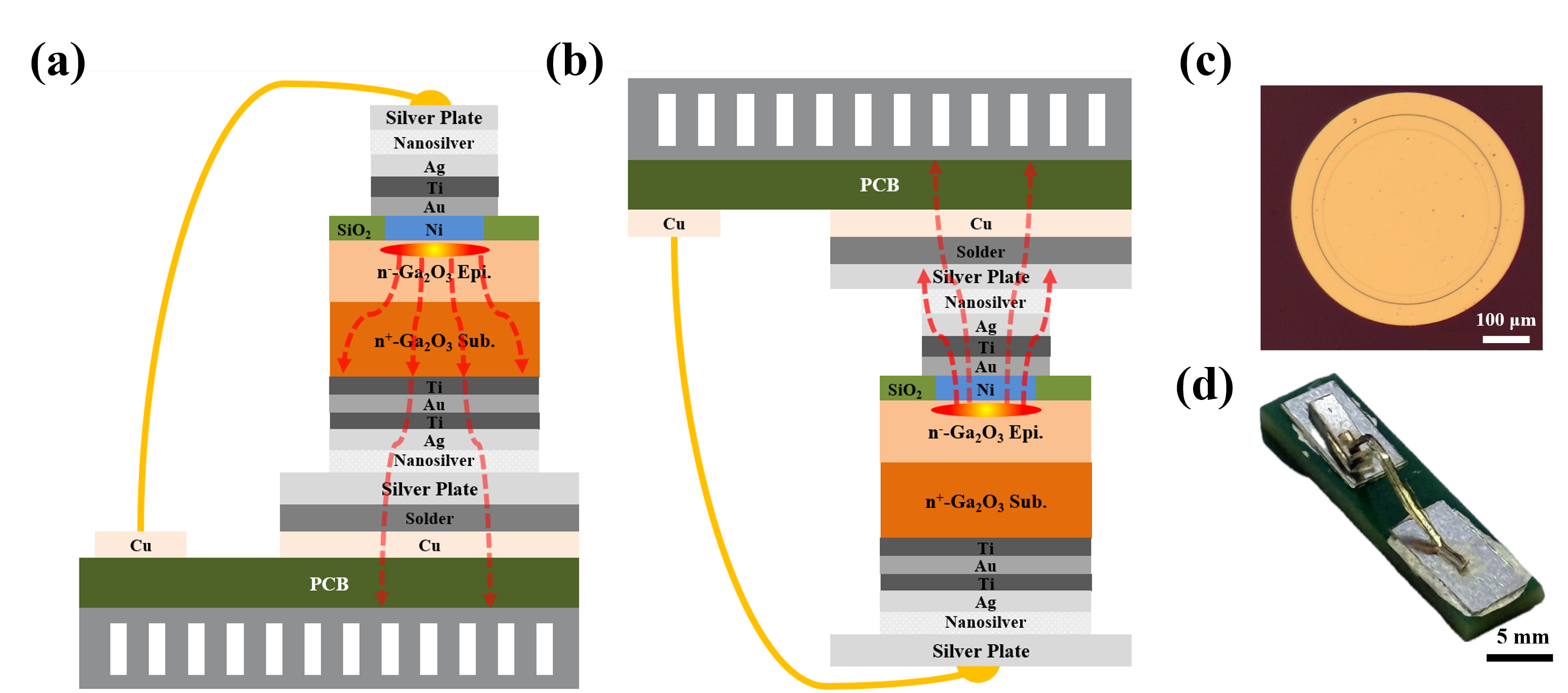
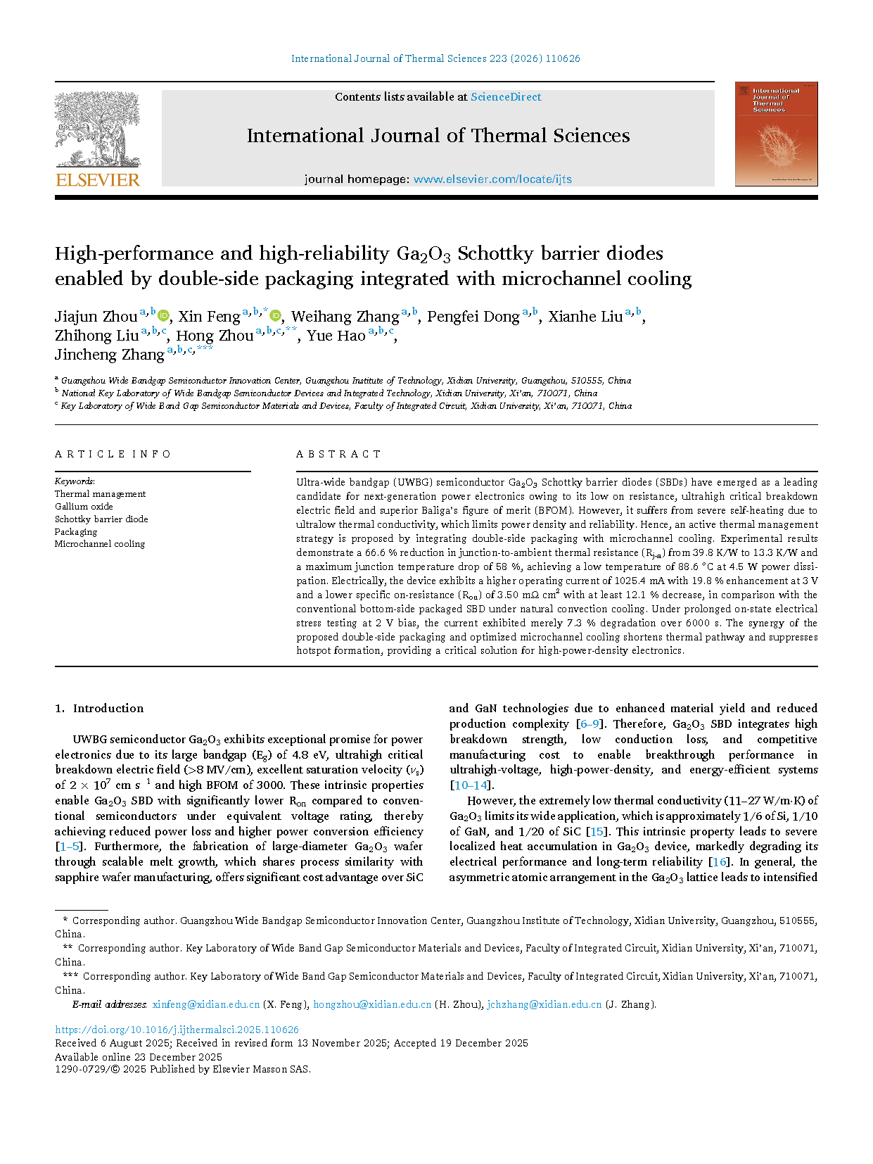
Fig. 1. Schematic of a vertical Ga2O3 SBD with integrated microchannel cooling, showing the configurations of (a) bottom-side and (b) double-side packaging. (c) Optical micrograph of the fabricated vertical Ga2O3 SBD. (d) Photograph of a double-side packaged vertical Ga2O3 SBD integrated with microchannel cooling.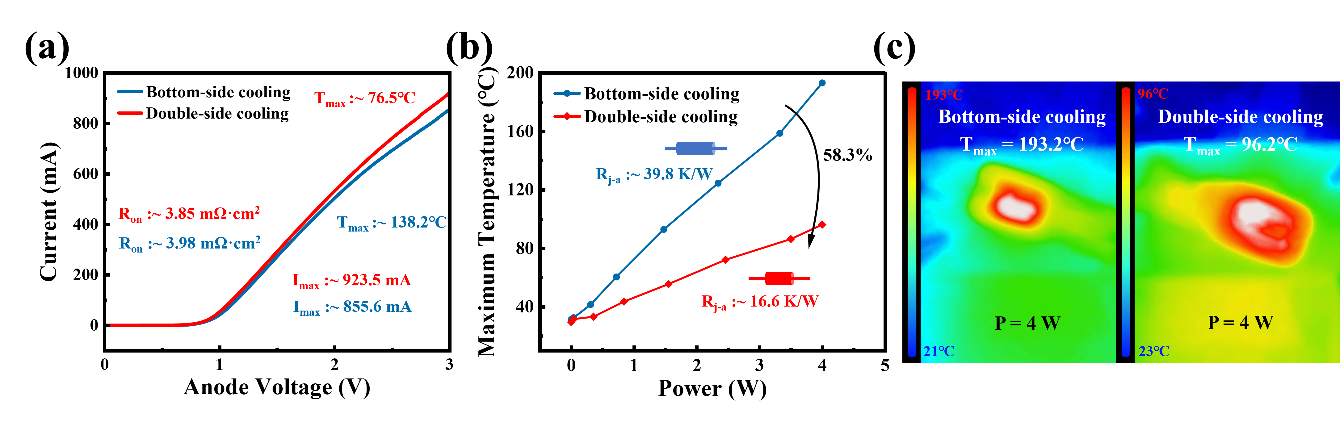
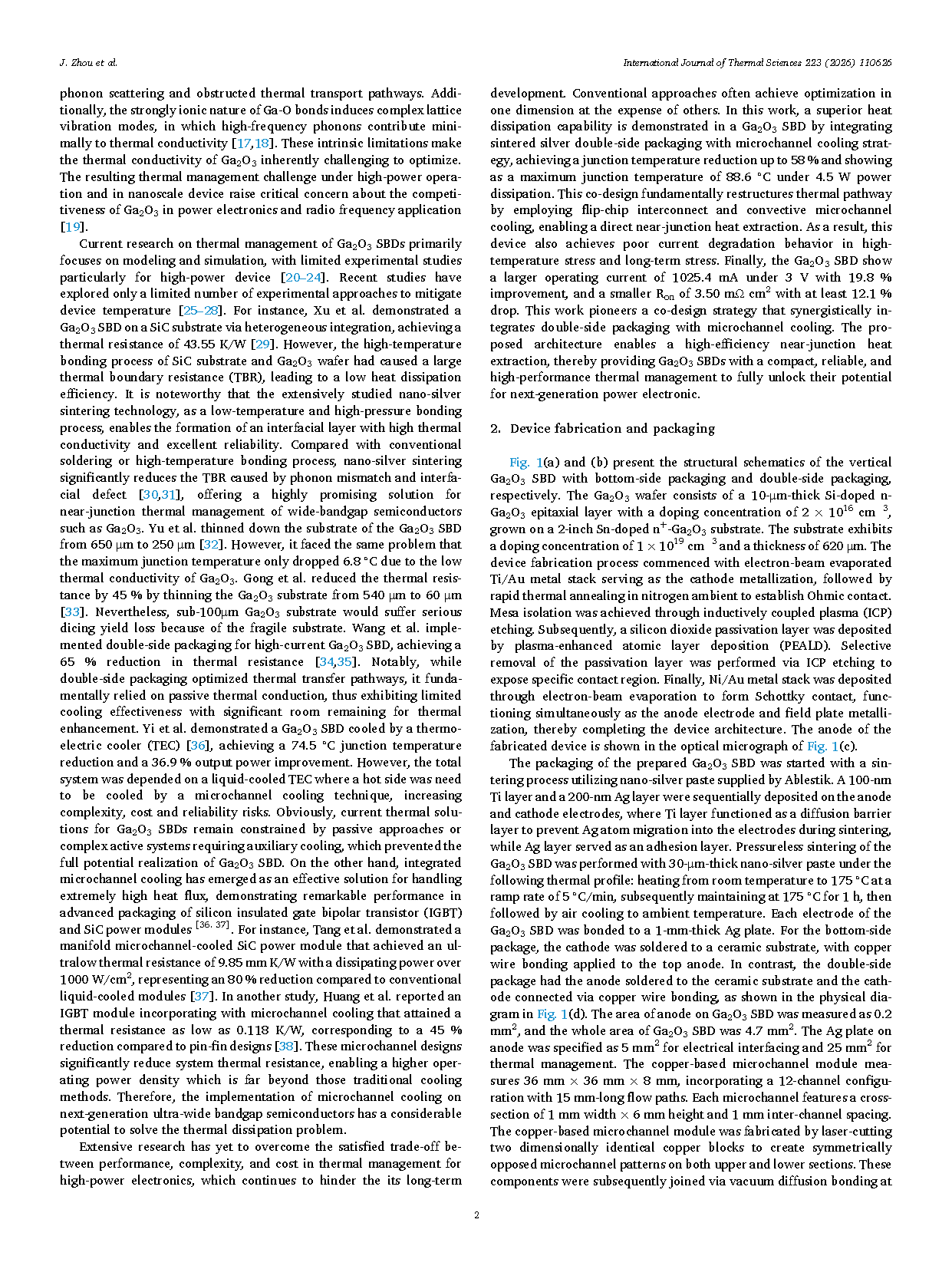
Fig. 2. (a) Forward I-V characteristics for double-side and bottom-side packaged devices. (b) Maximum surface temperature of two packaged devices versus power dissipation. (c) Infrared thermal images of device surfaces under 4 W power dissipation, bottom-side packaged device (left) and double-side packaged device (right).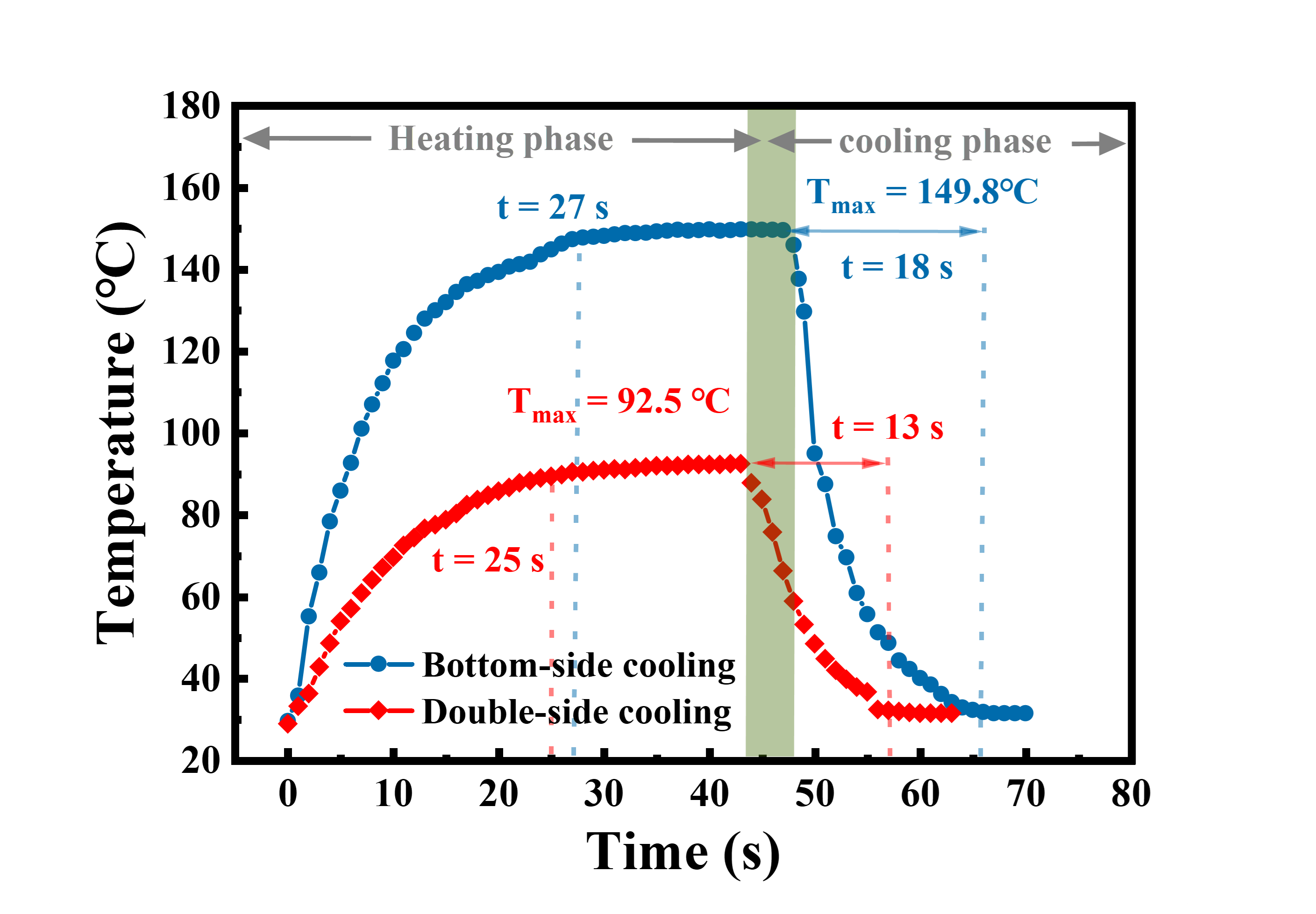
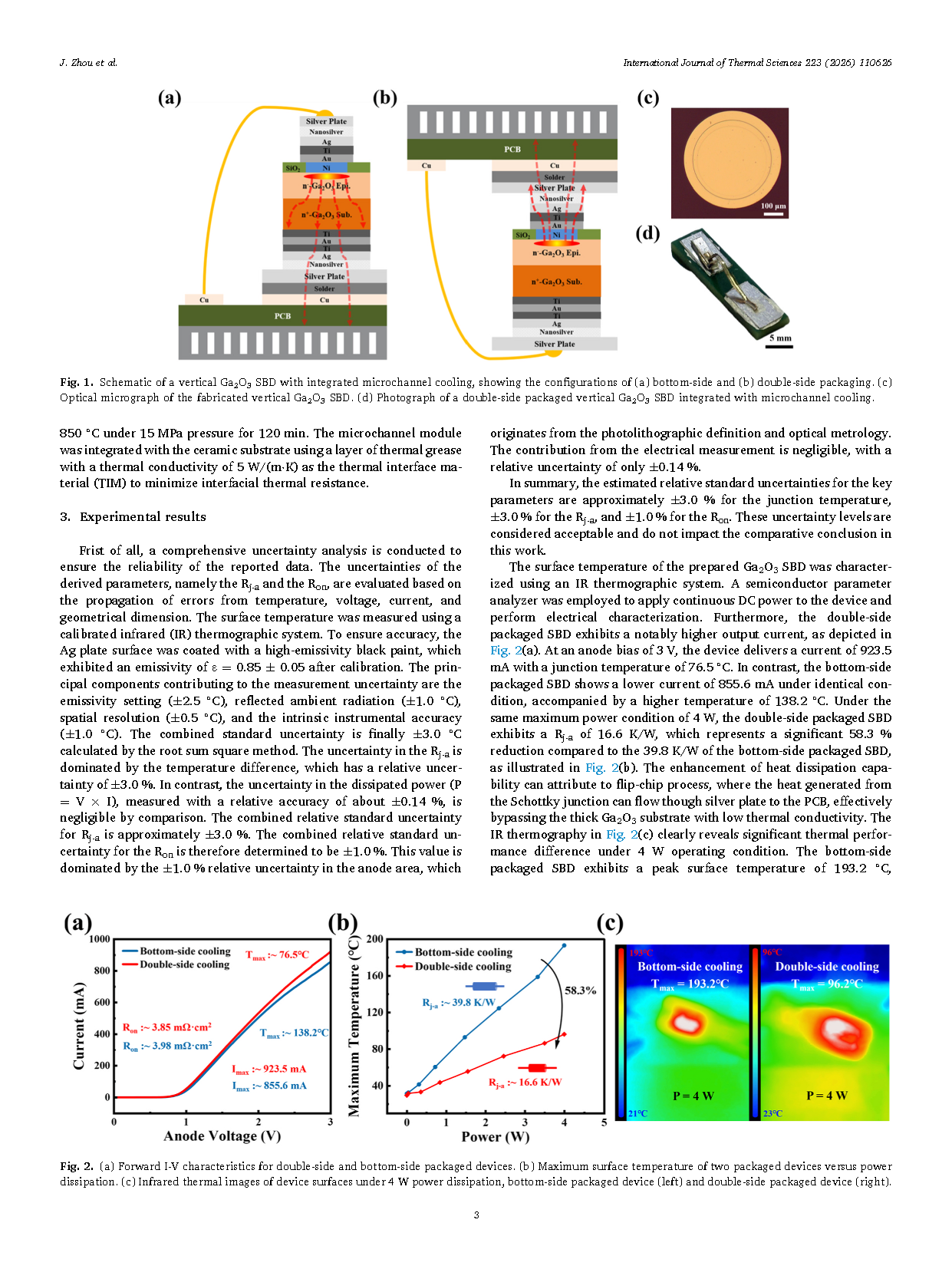
Fig. 3. Transient thermal response of devices under two packaged configurations: bottom-side packaged device at 2.8 W and double-side packaged device at 3.3 W.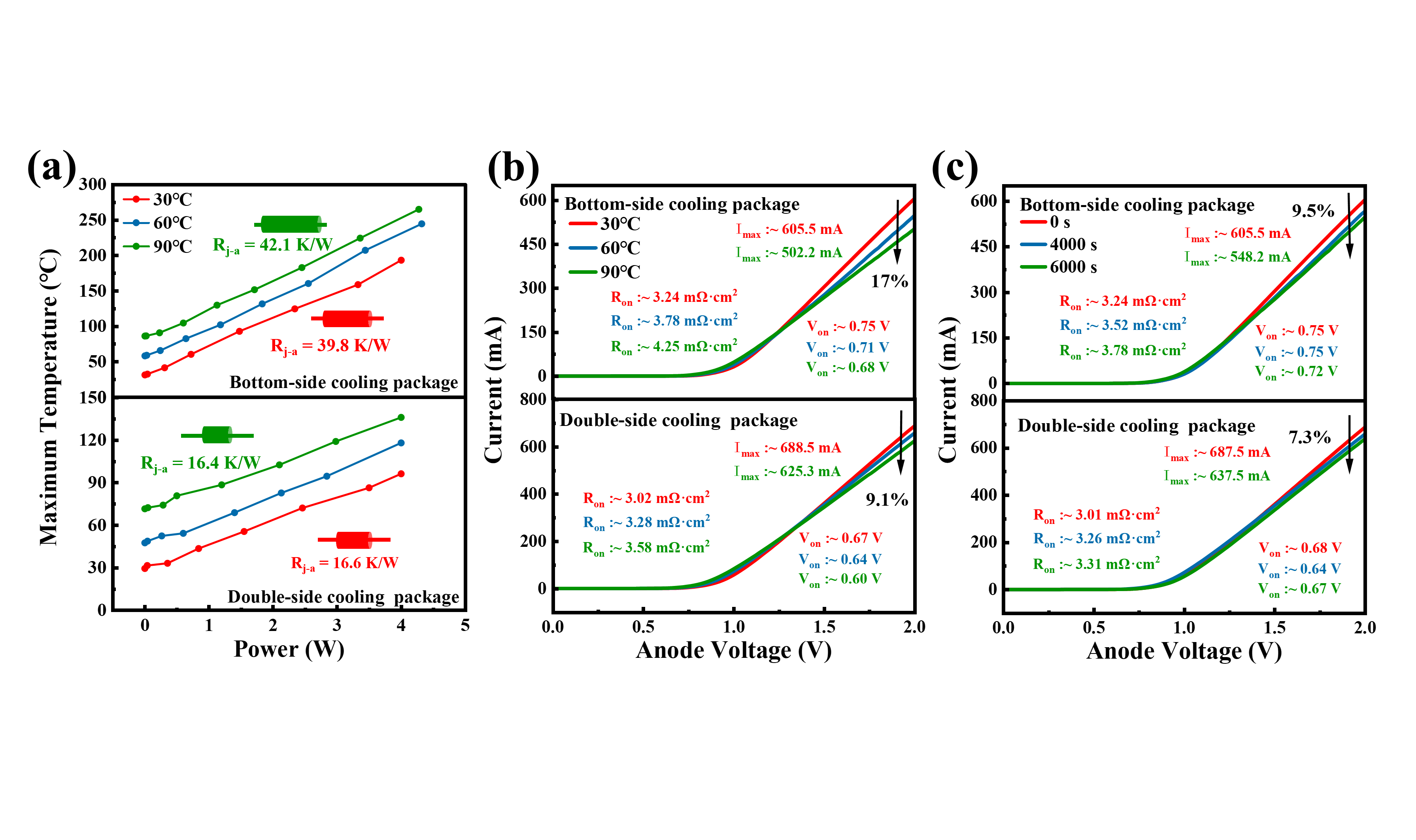
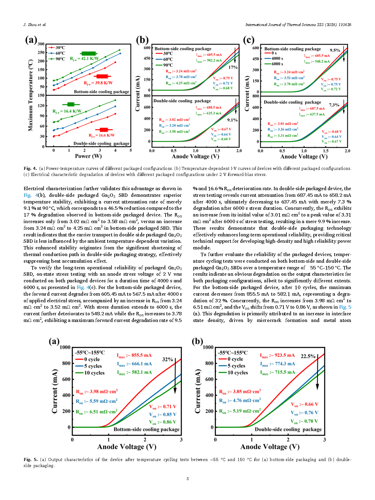
Fig. 4. (a) Power-temperature curves of different packaged configurations. (b) Temperature-dependent I-V curves of devices with different packaged configurations. (c) Electrical characteristic degradation of devices with different packaged configurations under 2 V forward-bias stress.
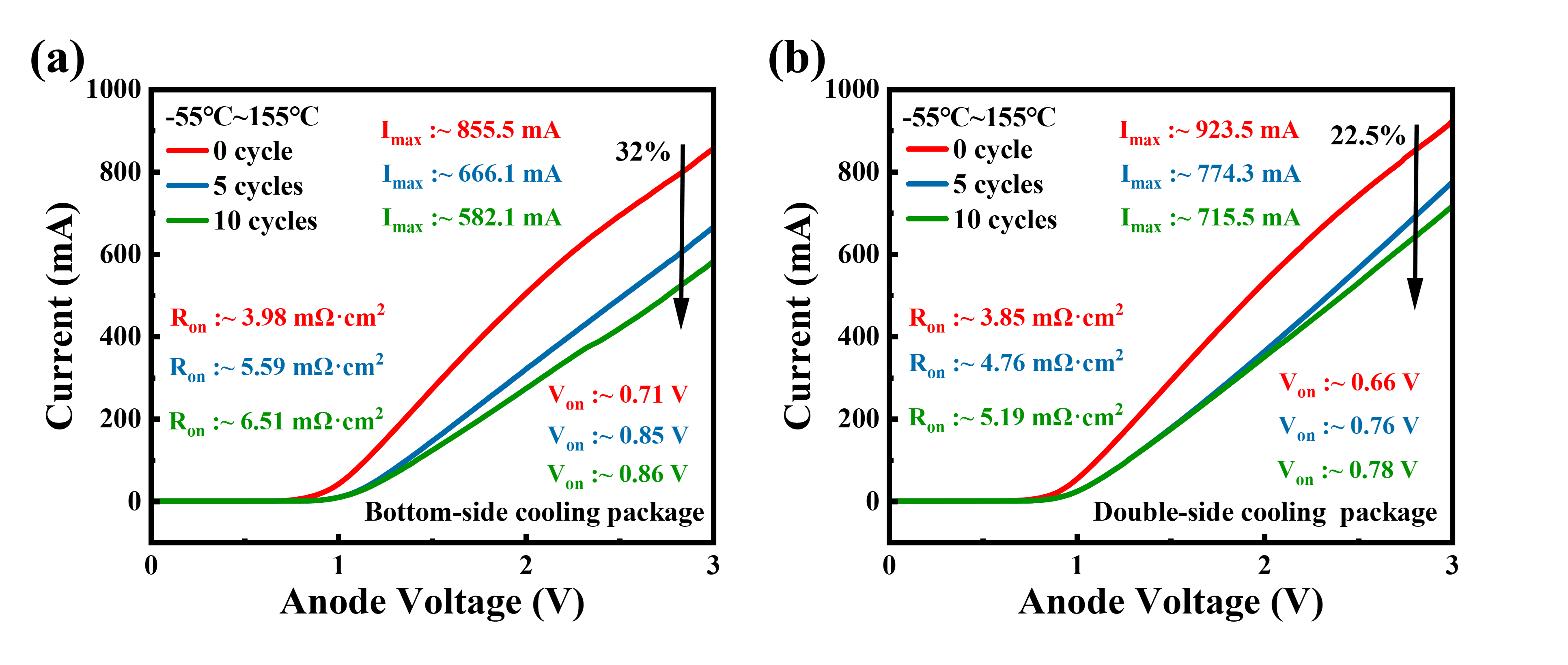
Fig. 5. (a) Output characteristics of the device after temperature cycling tests between − 55 °C and 150 °C for (a) bottom-side packaging and (b) double-side packaging.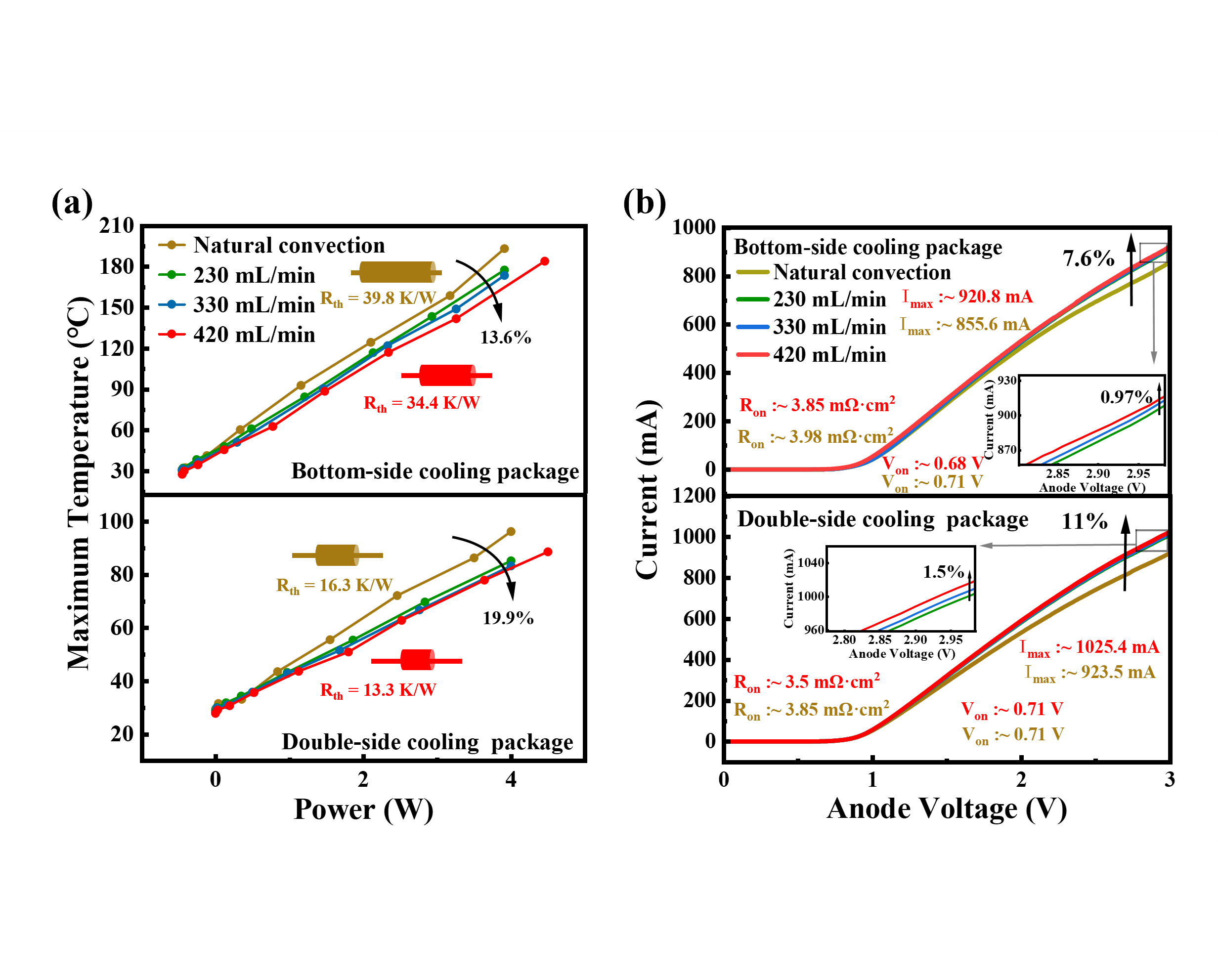
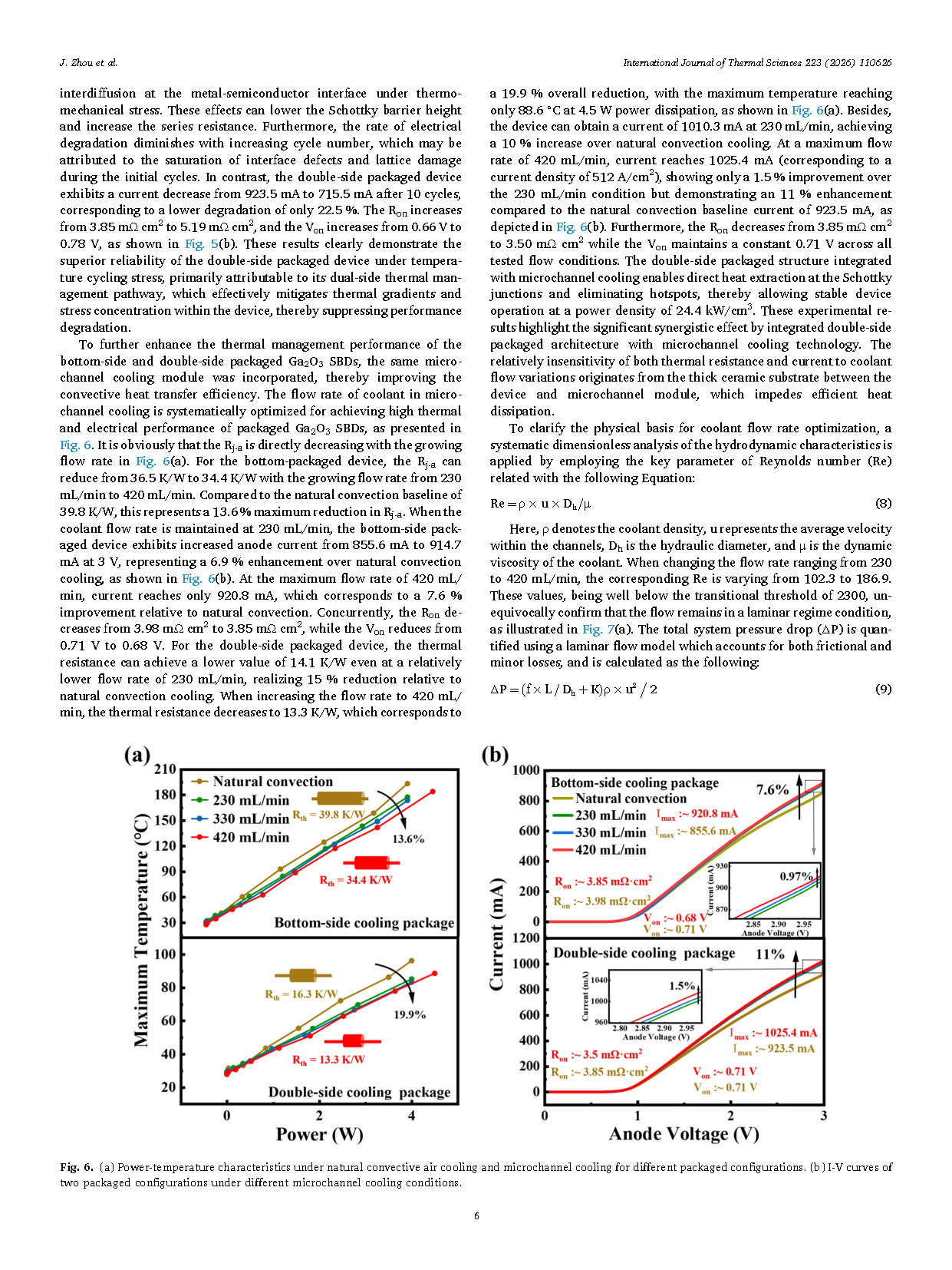
Fig. 6. (a) Power-temperature characteristics under natural convective air cooling and microchannel cooling for different packaged configurations. (b) I-V curves of two packaged configurations under different microchannel cooling conditions.
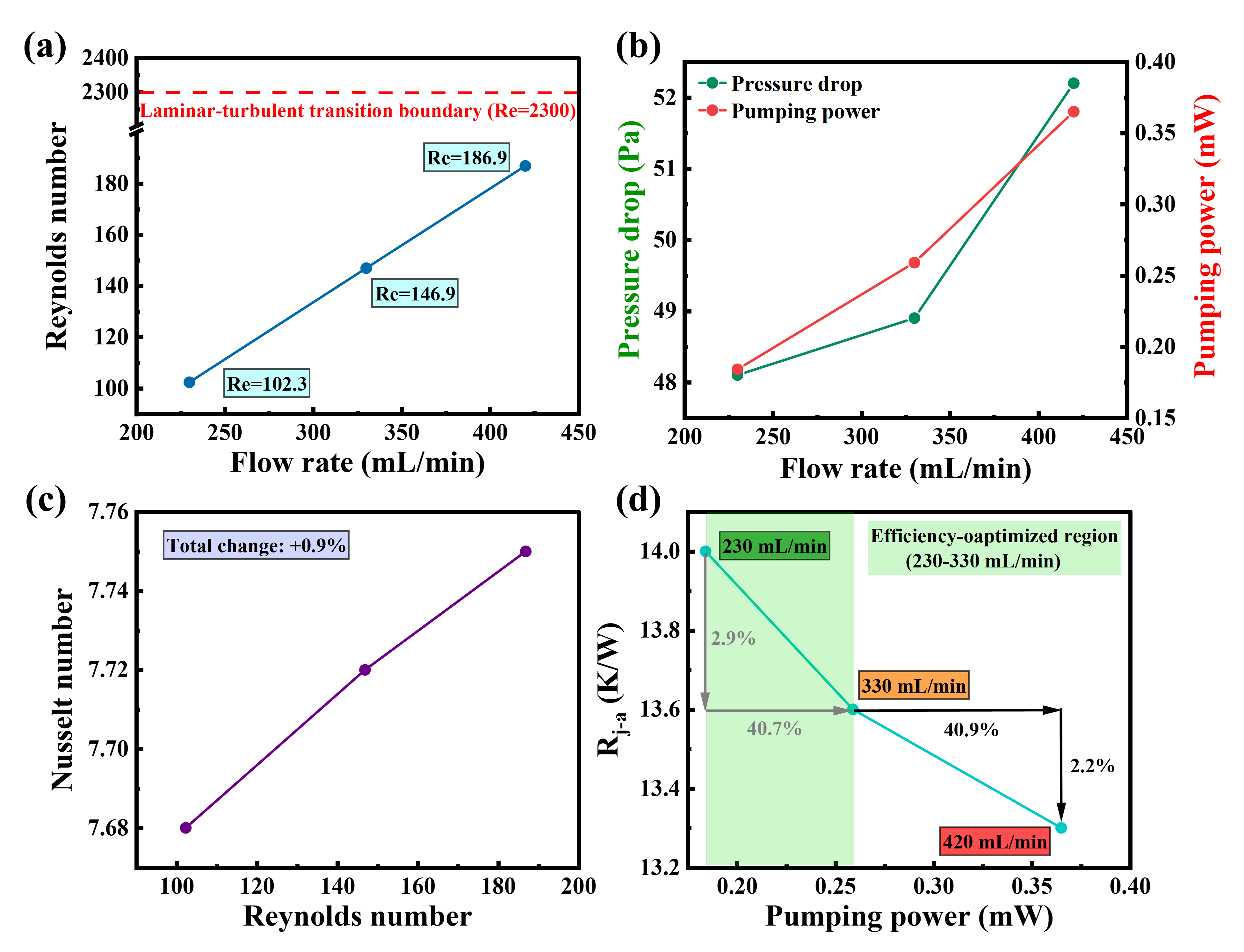
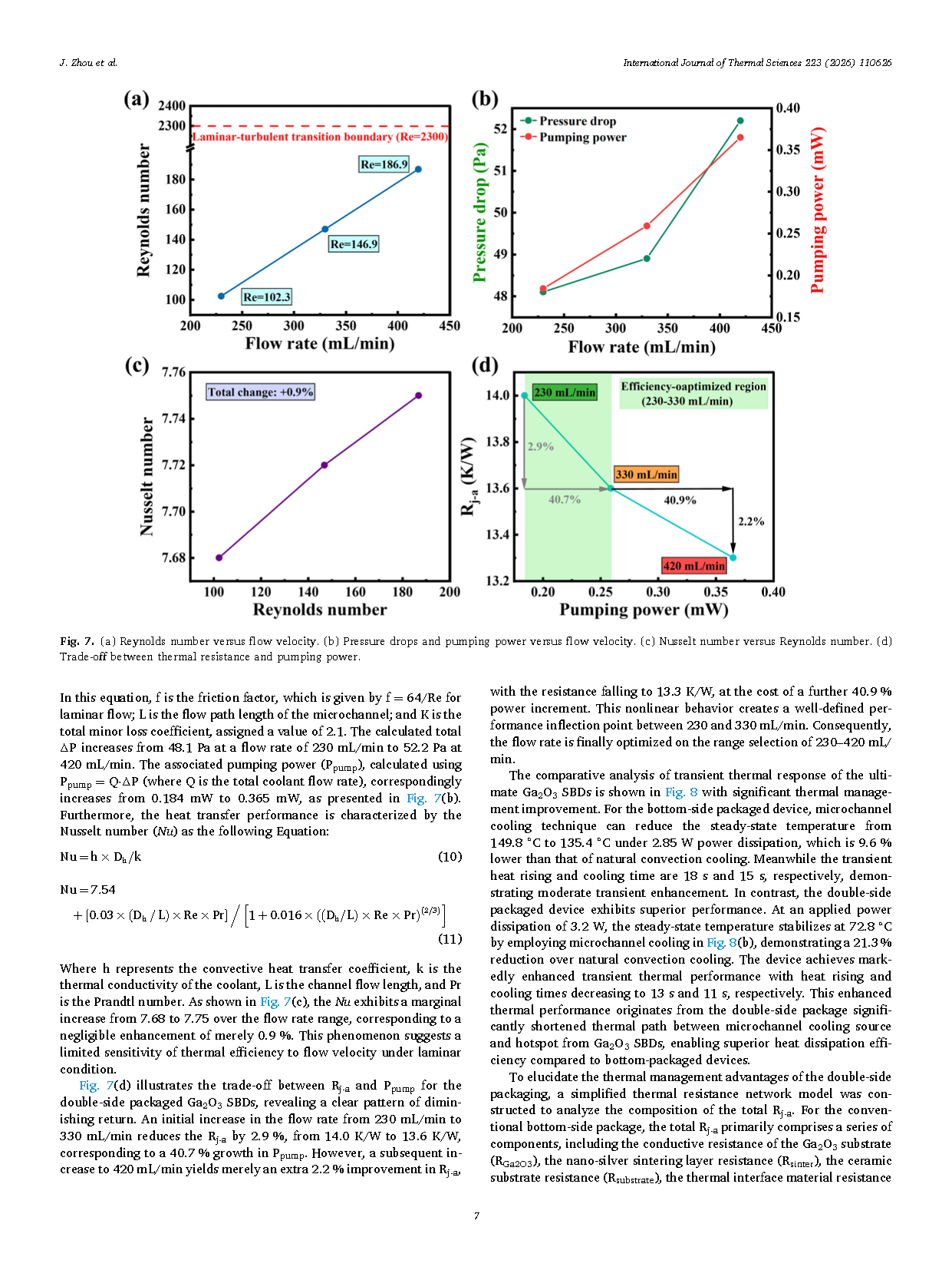
Fig. 7. (a) Reynolds number versus flow velocity. (b) Pressure drops and pumping power versus flow velocity. (c) Nusselt number versus Reynolds number. (d) Trade-off between thermal resistance and pumping power.
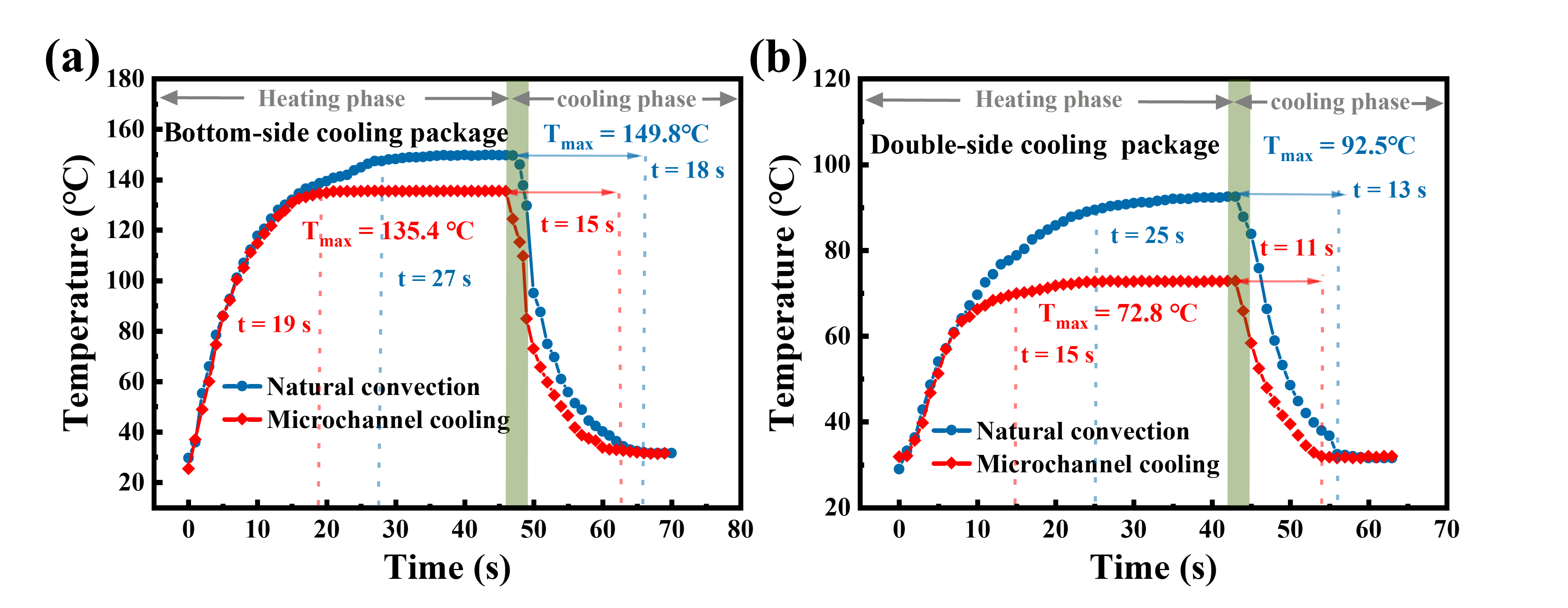
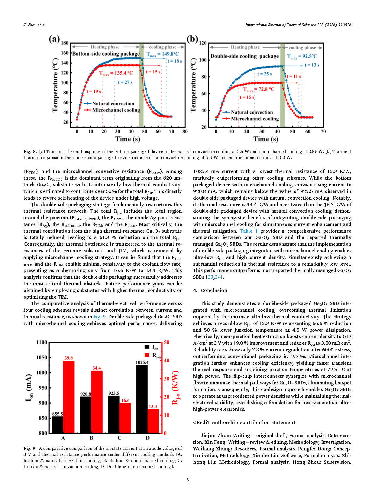
Fig. 8. (a) Transient thermal response of the bottom-packaged device under natural convection cooling at 2.8 W and microchannel cooling at 2.85 W. (b) Transient thermal response of the double-side packaged device under natural convection cooling at 3.3 W and microchannel cooling at 3.2 W.
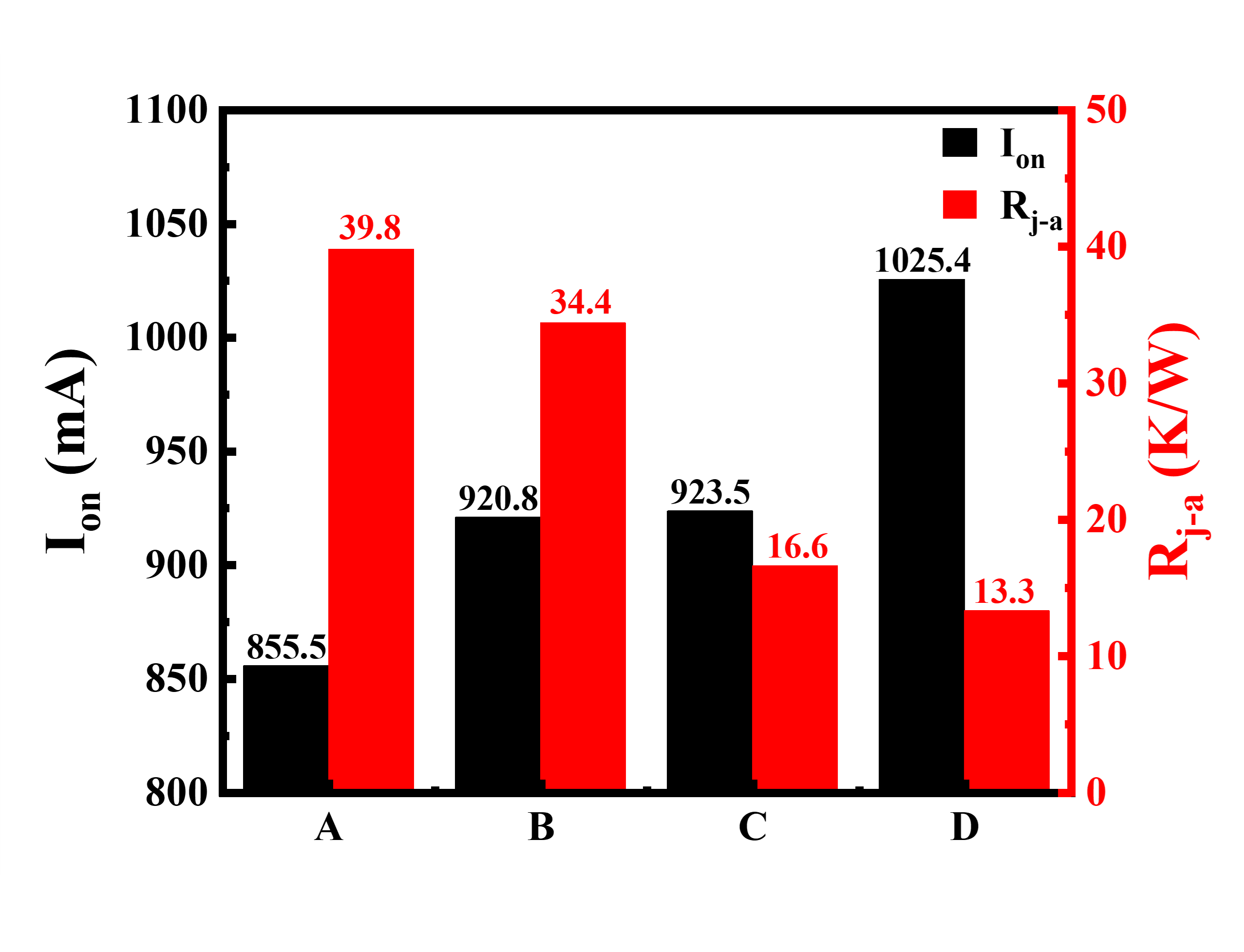
Fig. 9. A comparative comparison of the on-state current at an anode voltage of 3 V and thermal resistance performance under different cooling methods (A: Bottom & natural convection cooling; B: Bottom & microchannel cooling; C: Double & natural convection cooling; D: Double & microchannel cooling).
DOI:
doi.org/10.1016/j.ijthermalsci.2025.110626