Paper Sharing
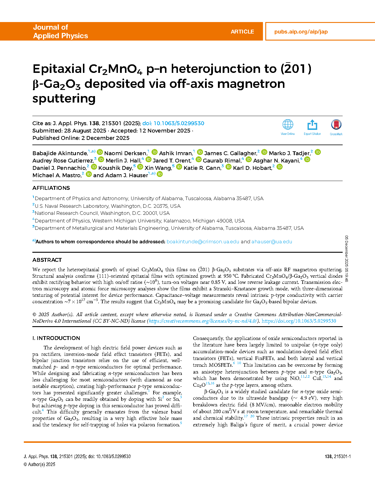
【International Papers】Epitaxial Cr₂MnO₄ p–n heterojunction to (-201) β-Ga₂O₃ deposited via off-axis magnetron sputtering
日期:2026-01-05阅读:409
Researchers from the Journal of Applied Physics have published a dissertation titled "Epitaxial Cr2MnO4 p–n heterojunction to (-201) β-Ga2O3 deposited via off-axis magnetron sputtering" in Journal of Applied Physics.
Background
The development of high electric field power devices such as pn rectifiers, inversion-mode field effect transistors (FETs), and bipolar junction transistors relies on the use of efficient, well-matched p- and n-type semiconductors for optimal performance. While designing and fabricating n-type semiconductors has been less challenging for most semiconductors (with diamond as one notable exception), creating high-performance p-type semiconductors has presented significantly greater challenges. For example, n-type Ga2O3 can be readily obtained by doping with Si or Sn, but achieving p-type doping in this semiconductor has proved difficult. This difficulty generally emanates from the valence band properties of Ga2O3, resulting in a very high effective hole mass and the tendency for self-trapping of holes via polaron formation. Consequently, the applications of oxide semiconductors reported in the literature have been largely limited to unipolar (n-type only) accumulation-mode devices such as modulation-doped field effect transistors (FETs), vertical FinFETs, and both lateral and vertical trench MOSFETs. This limitation can be overcome by forming an anisotype heterojunction between p-type and n-type Ga2O3, which has been demonstrated by using NiO, CuI, and Cu2O as the p-type layers, among others.
Abstract
We report the heteroepitaxial growth of spinel Cr2MnO4 thin films on (-201) β-Ga2O3 substrates via off-axis RF magnetron sputtering. Structural analysis confirms (111)-oriented epitaxial films with optimized growth at 950 °C. Fabricated Cr2MnO4/β-Ga2O3 vertical diodes exhibit rectifying behavior with high on/off ratios (∼108), turn-on voltages near 0.85 V, and low reverse leakage current. Transmission electron microscopy and atomic force microscopy analyses show the films exhibit a Stranski–Krastanov growth mode, with three-dimensional texturing of potential interest for device performance. Capacitance–voltage measurements reveal intrinsic p-type conductivity with carrier concentration ∼7 × 1017 cm−3. The results suggest that Cr2MnO4 may be a promising candidate for Ga2O3-based bipolar devices.
Conclusion
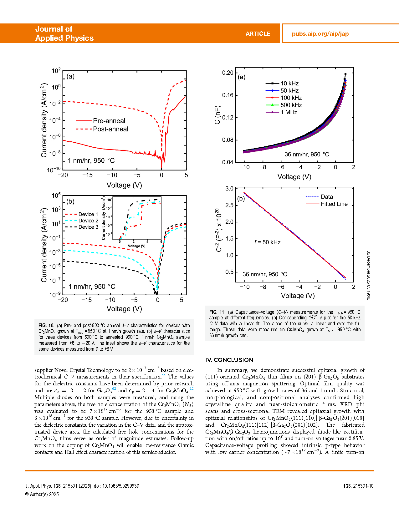
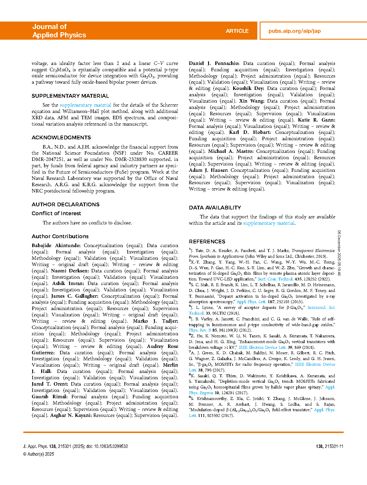
In summary, we demonstrate successful epitaxial growth of (111)-oriented Cr2MnO4 thin films on (-201) β-Ga2O3 substrates using off-axis magnetron sputtering. Optimal film quality was achieved at 950 °C with growth rates of 36 and 1 nm/h. Structural, morphological, and compositional analyses confirmed high crystalline quality and near-stoichiometric films. XRD phi scans and cross-sectional TEM revealed epitaxial growth with epitaxial relationships of Cr2MnO4 (111) [1-10] || β-Ga2O3 (-201) [010] and Cr2MnO4 (111) [-1-12] || β-Ga2O3 (-201) [102]. The fabricated Cr2MnO4/β-Ga2O3 heterojunctions displayed diode-like rectification with on/off ratios up to 108 and turn-on voltages near 0.85 V. Capacitance–voltage profiling showed intrinsic p-type behavior with low carrier concentration (∼7 × 1017 cm−3). A finite turn-on voltage, an ideality factor less than 2 and a linear C–V curve suggest Cr2MnO4 is epitaxially compatible and a potential p-type oxide semiconductor for device integration with Ga2O3, providing a pathway toward fully oxide-based bipolar power devices.
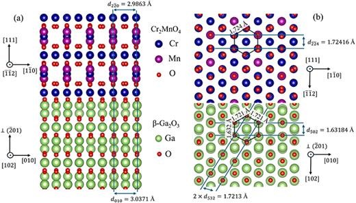
FIG. 1. Schematic diagrams showing (a) cross-sectional views of the proposed epitaxial alignment between the (111) plane of spinel Cr2MnO4 and the (-201) plane of β-Ga2O3, and (b) top views of the Cr2MnO4 (111) and β-Ga2O3 (-201) planes. Hexagonal arrangements of O atoms are observed in the Cr2MnO4 (111) plane, with a side length of 1.724 Å, and in the β-Ga2O3 (-201) plane, with side lengths ranging from 1.632 to 1.721Å. The crystal structure models were generated using the Crystallographic Information Files (CIFs) obtained from the Inorganic Crystal Structure Database (ICSD).
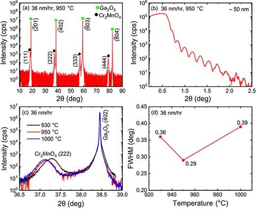
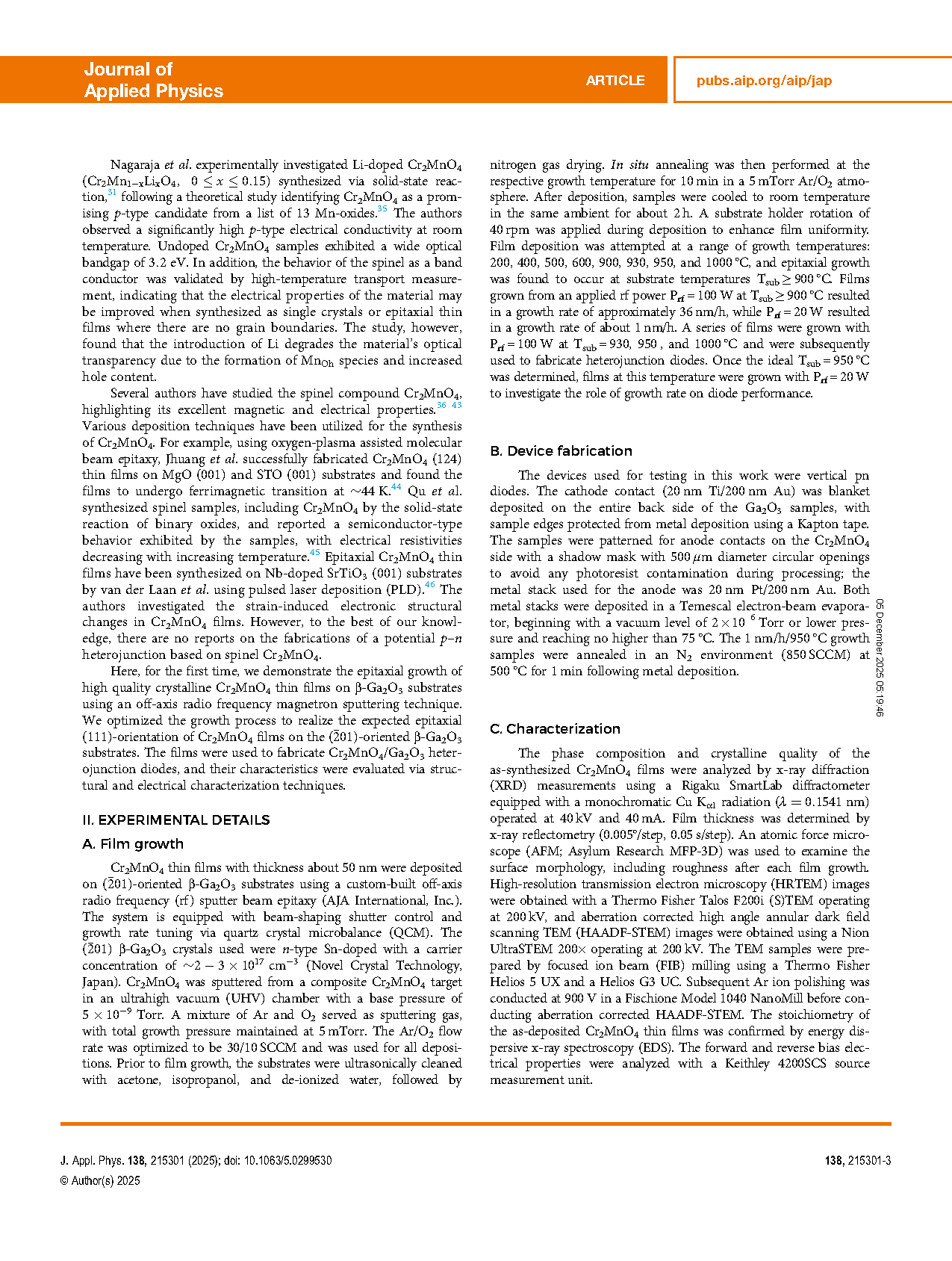
FIG. 2. (a) Typical 2θ–ω XRD pattern of the film grown at 36 nm/h and 950 °C. Black circles denote the peaks corresponding to Cr2MnO4, while green squares denote the peaks corresponding to the β-Ga2O3 substrate. (b) 2θ–ω XRR scan of the sample. Film thickness was calculated to be about 50 nm. (c) Expanded views of (222) diffraction peaks of films grown at different temperatures with 36 nm/h. (d) FWHM values of the Cr2MnO4 (222) diffraction peak as a function of growth temperature.
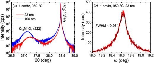
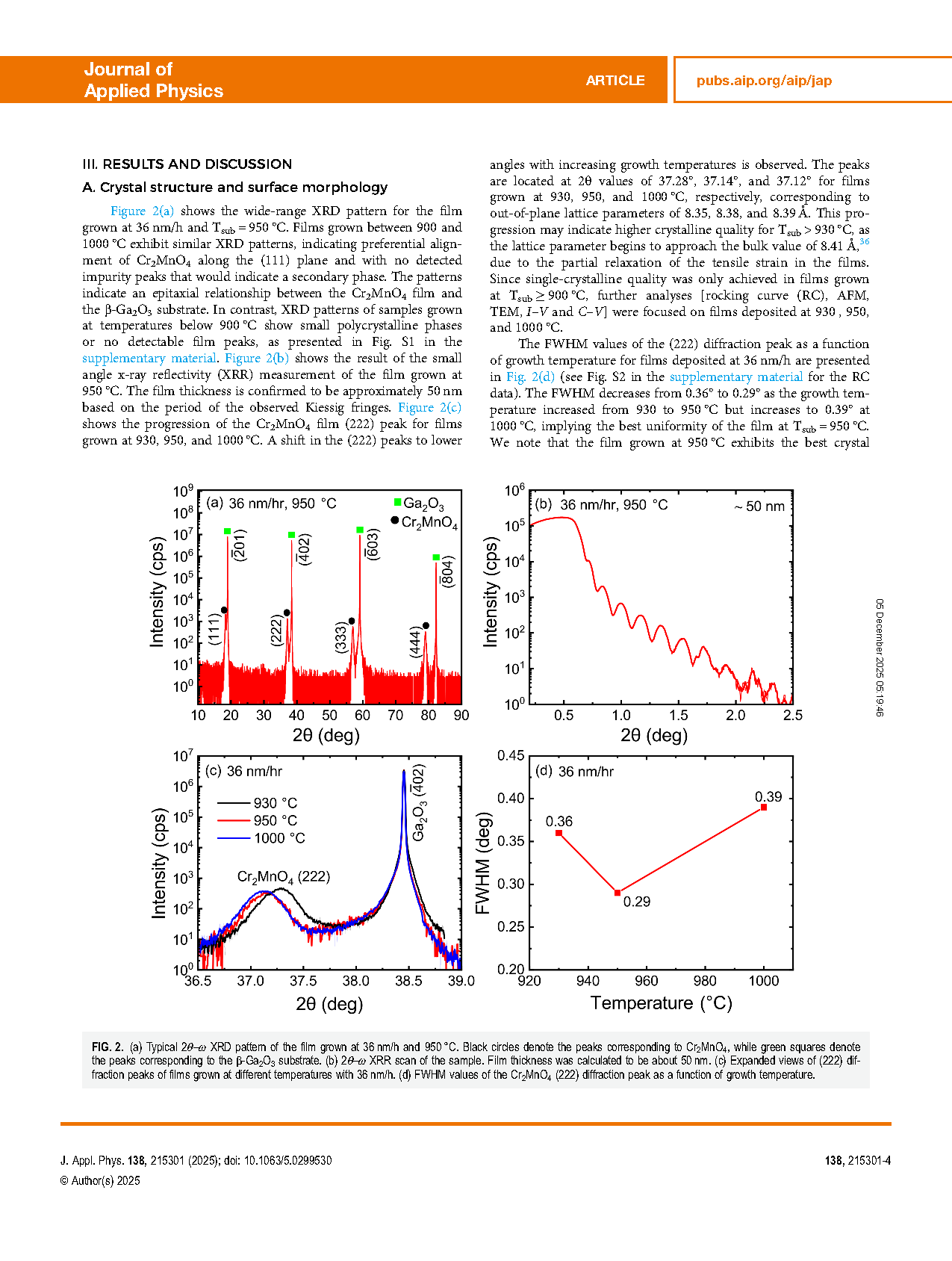
FIG. 3. (a) Expanded views of (222) diffraction peaks of films grown at 950 °C with 1 nm/h. (b) Rocking curve for the (222) Bragg peak of the 23 nm film. The corresponding fit is presented in black color with FWHM determined to be ∼0.26°.
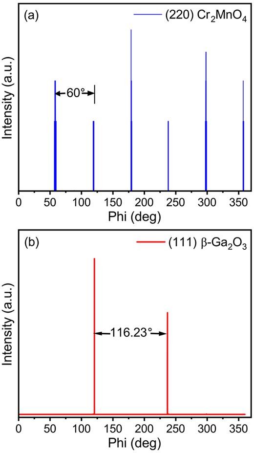
FIG. 4. In-plane phi scans of (a) (220) plane of the Cr2MnO4 film (1000 °C) and (b) (111) plane of the β-Ga2O3 substrate.
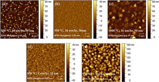
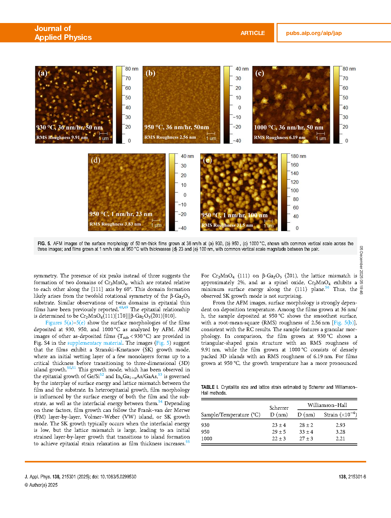
FIG. 5. AFM images of the surface morphology of 50 nm-thick films grown at 36 nm/h at (a) 930, (b) 950 , (c) 1000 °C, shown with common vertical scale across the three images; and films grown at 1 nm/h rate at 950 °C with thicknesses (d) 23 and (e) 100 nm, with common vertical scale magnitude between the pair.
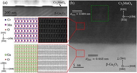
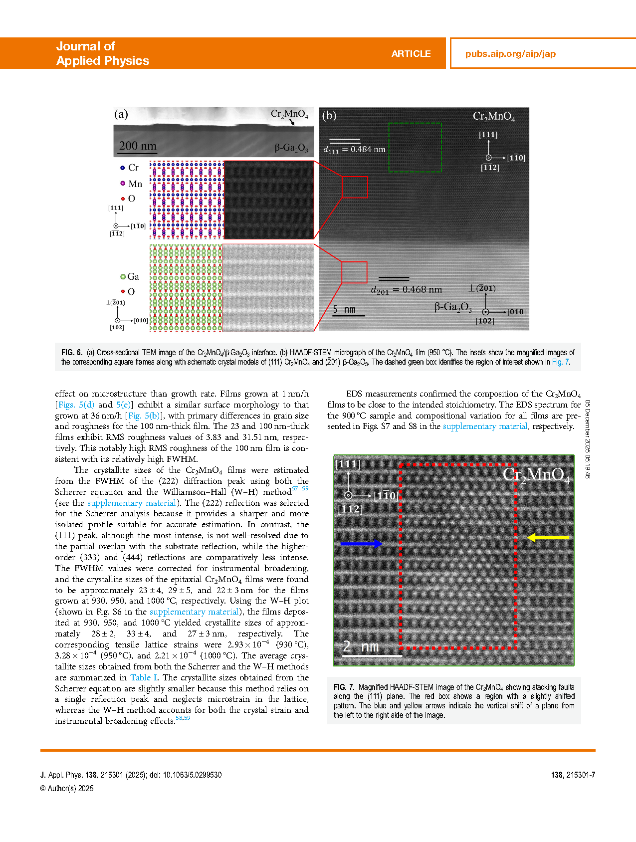
FIG. 6. (a) Cross-sectional TEM image of the Cr2MnO4/β-Ga2O3 interface. (b) HAADF-STEM micrograph of the Cr2MnO4 film (950 °C). The insets show the magnified images of the corresponding square frames along with schematic crystal models of (111) Cr2MnO4 and (-201) β-Ga2O3.
DOI:
doi.org/10.1063/5.0299530