Paper Sharing
【Domestic Papers】Influence of the number of growth cycles on the solar-blind photoresponse of amorphous and crystalline Ga₂O₃ films by atomic layer deposition
日期:2026-01-06阅读:420
Researchers from the Xi'an University of Posts & Telecommunications have published a dissertation titled "Influence of the number of growth cycles on the solar-blind photoresponse of amorphous and crystalline Ga2O3 films by atomic layer deposition" in Materials Science and Engineering: B.
Project Support
This work was supported by the National Natural Science Foundation of China (Grant No. 62304178) and Natural Science Basic Research Program of Shaanxi Province (Grant No. 2022JQ-684).
Background
Solar-blind photodetectors, which are specifically sensitive to the 200–280 nm ultraviolet band, have attracted significant interest for applications including missile plume detection, corona discharge monitoring, and flame sensing, owing to their inherent solar blindness and reliable operation under strong background illumination. Among wide-bandgap semiconductors, gallium oxide (Ga2O3) has emerged as a highly promising material for solar-blind photodetectors, thanks to its tunable ultra-wide bandgap (4.4–5.3 eV) [4], which aligns naturally with the solar-blind window without requiring complex bandgap engineering. It also possesses advantages such as high-temperature resistance, UV radiation resistance, high voltage resistance, and good chemical stability, making it gradually become a research hotspot in the field of solar-blind UV detection.
In this work, amorphous and crystalline Ga2O3 films of varying thicknesses were deposited on sapphire substrates via atomic layer deposition to fabricate metal-semiconductor-metal (MSM) solar-blind photodetectors. A key finding is the observed saturation of photocurrent/responsivity in amorphous Ga2O3 PDs beyond a critical thickness, in stark contrast to the monotonic increase exhibited in crystalline Ga2O3 within the studied range. Also, our work provides a direct parallel comparison of amorphous and crystalline Ga₂O₃ PDs with the same thickness. These findings provide valuable guidance for engineering Ga₂O₃-based photodetectors, highlighting the significant role of material phases and film thickness in influencing device performance.
Abstract
This study investigates the photodetection performance of amorphous Ga2O3 and crystalline films grown by atomic layer deposition with varying growth cycles (1000–7000 cycles). The fundamental difference in structural order – long-range in crystalline versus short-range in amorphous - governs their distinct optoelectronic behaviors. For amorphous Ga2O3 devices, photocurrent/responsivity nealrly saturates beyond a certain thickness. This limitation comes from low carrier mobility and short diffusion length due to abundant trap states. In contrast, crystalline Ga2O3 photodetectors show a monotonic increase in responsivity with film thickness, benefiting from its long-range order which contributes to a longer carrier diffusion length and superior charge collection efficiency. Consequently, for thinner films, the high photoconductive gain from carrier trapping in amorphous films leads to higher responsivity for amorphous Ga2O3 photodetecors. However, for thicker films, the photoresponsivity and response speed of crystalline Ga2O3 photodetectors are both superior to those of amorphous Ga2O3 photodetectors. These advantages can be attributed to the greater absorption depth and longer carrier diffusion length. This work establishes how the material phase (amorphous vs. crystalline) and film thickness jointly influence the performance of Ga2O3 photodetectors. The obtained results provide valuable insights for the design of Ga2O3 photodetectors.
Highlights
● Saturation of the photoresponsivity in amorphous Ga2O3 is observed for the first time as the film thickness increases.
● The photoresponsivity of crystalline Ga2O3 PDs increases monotonically as a function of the number of growth cycles.
● A parallel comparison of amorphous and crystalline Ga2O3 PDs is provided across a wide range of ALD cycles.
Conclusions
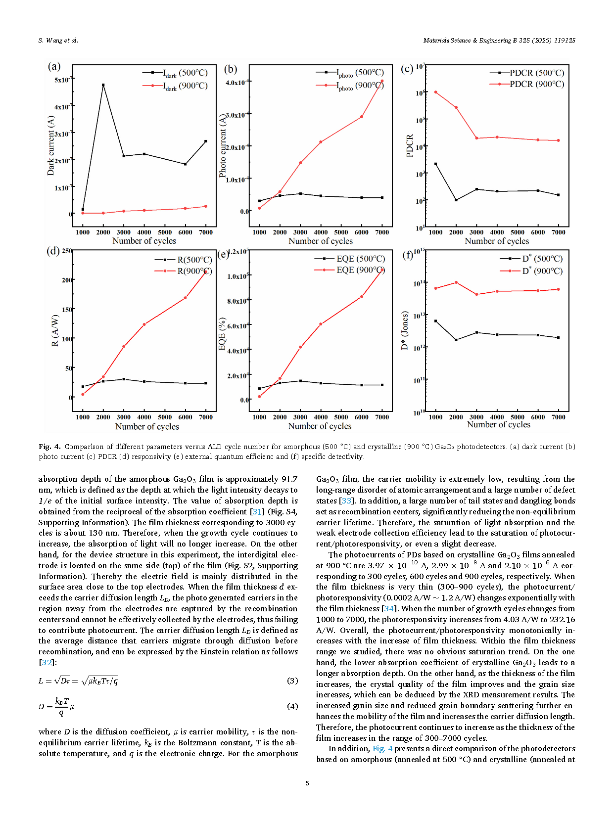
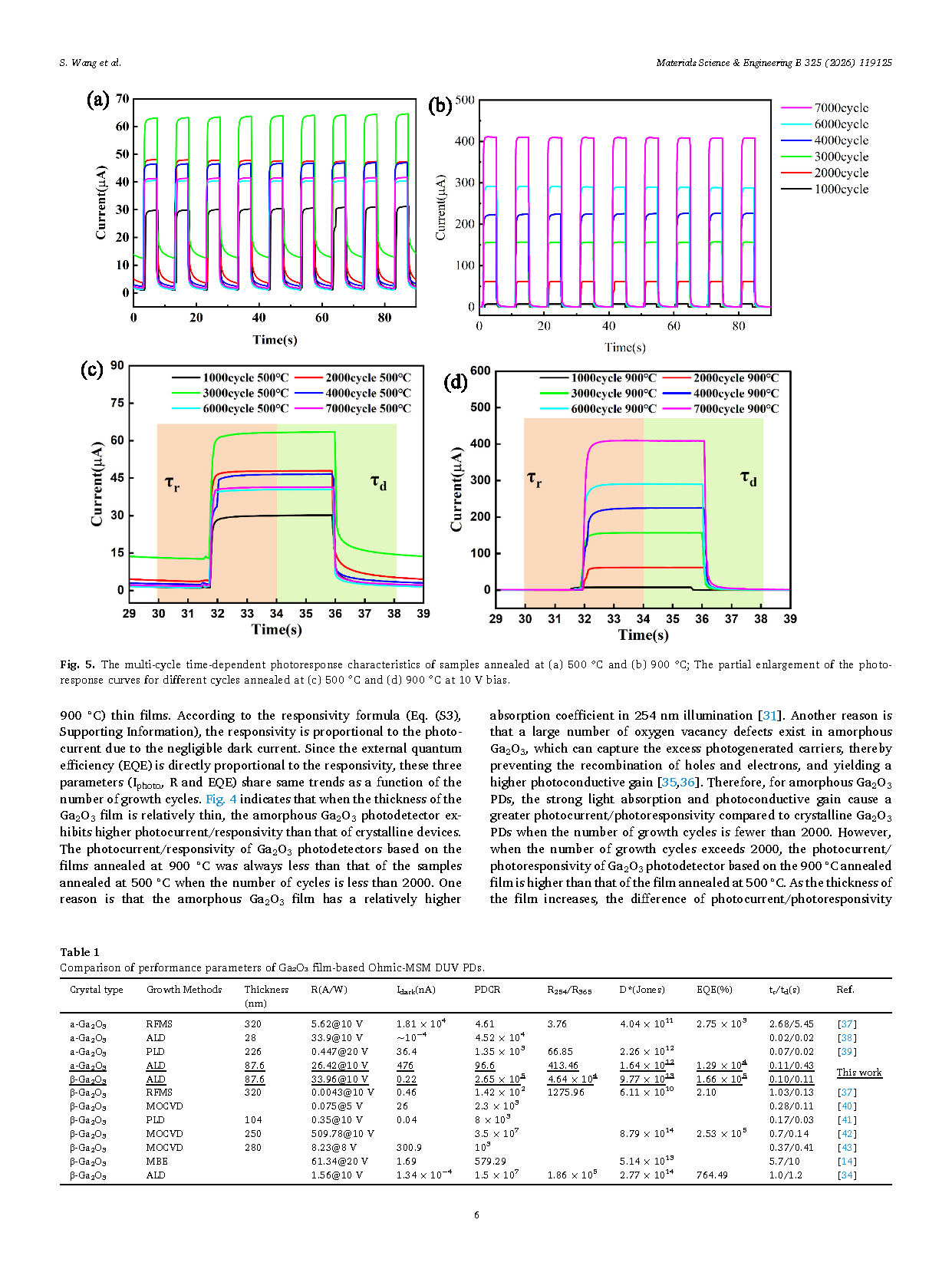
In conclusion, this work systematically elucidates the distinct thickness-dependent photoresponse of amorphous and crystalline Ga2O3 photodetectors prepared by atomic layer deposition. The primary finding is a fundamental divergence in behavior: the photocurrent/responsivity of amorphous Ga2O3 saturates beyond a critical thickness (∼130 nm), whereas the photocurrent/responsivity of crystalline Ga2O3 PDs increases monotonically across the studied range (up to ∼300 nm). This contrast is governed by the inherent structural disorder of the amorphous phase. The low mobility and short carrier diffusion length in a-Ga2O3, induced by abundant trap states limits the charge collection efficiency by the electrodes, leading to the saturation of the photocurrent/responsivity. Conversely, the long-range order in crystalline Ga2O3 facilitates a higher mobility, a longer carrier diffusion length and superior charge collection efficiency, enabling sustained performance improvement with increasing thickness. This study also provides a parallel comparison of amorphous and crystalline Ga2O3 PDs with the same film thickness. When the film thickness is relatively thin, due to the significant difference of absorption coefficients and photoconductive gain between amorphous and crystalline state, the photoresponsivity after 500 ◦C annealing is greater than that after 900 ◦C annealing. However, when the film is relatively thick, the photoresponsivity and response speed of crystalline Ga2O3 photodetector are both superior to those of amorphous Ga2O3 photodetector. These insights deliver a crucial design rule: amorphous Ga2O3 is suited for cost-effective, low-speed applications in thin-film form, while crystalline Ga2O3 is optimal for high-responsivity and high-speed devices, underscoring the critical role of material phase in device engineering.
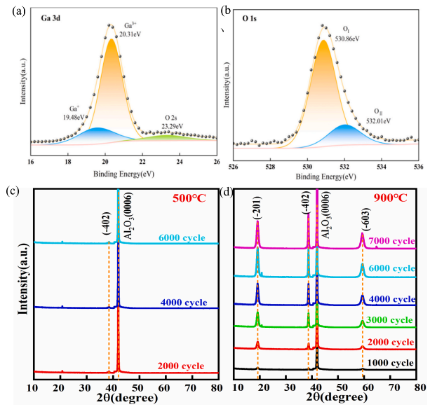
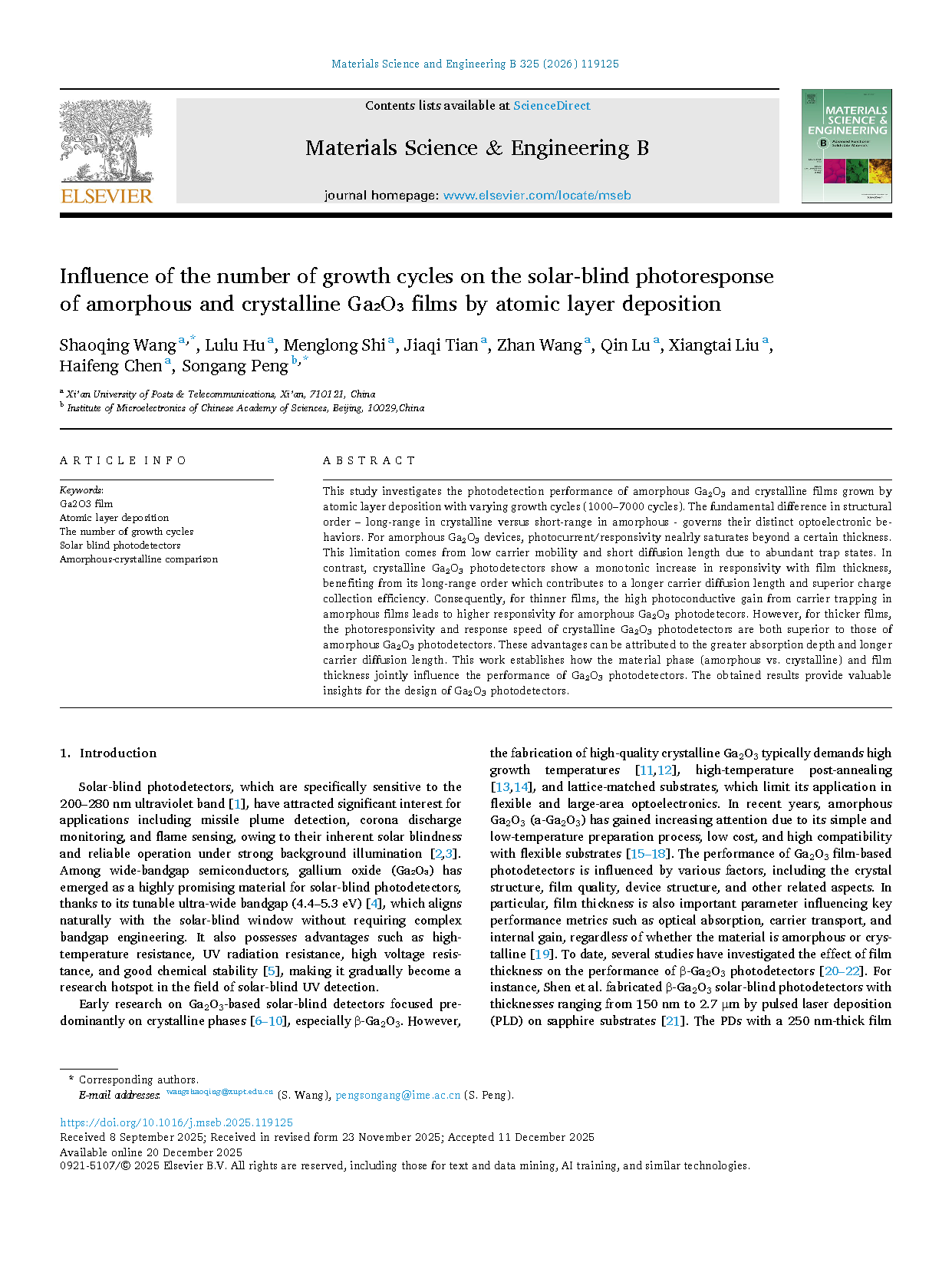
Fig. 1. XPS spectra of as-grown Ga2O3 films on sapphire substrate: (a) Ga 3d and (b) O 1s. XRD patterns of Ga2O3 films (a) annealed at 500 ◦C and (b) annealed at 900 ◦C.
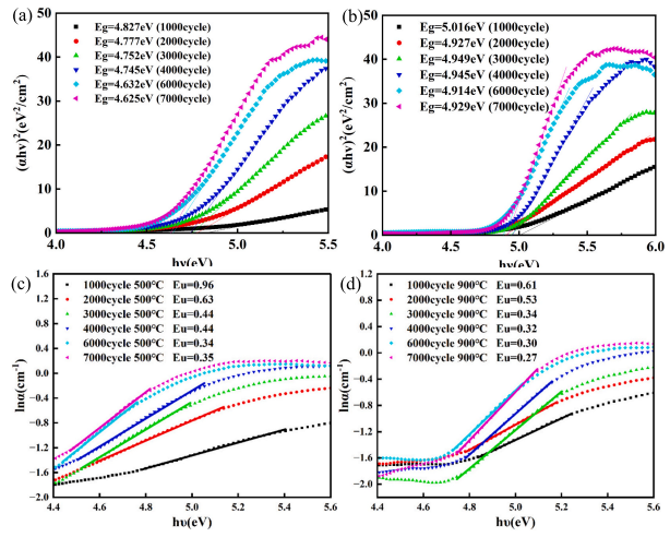
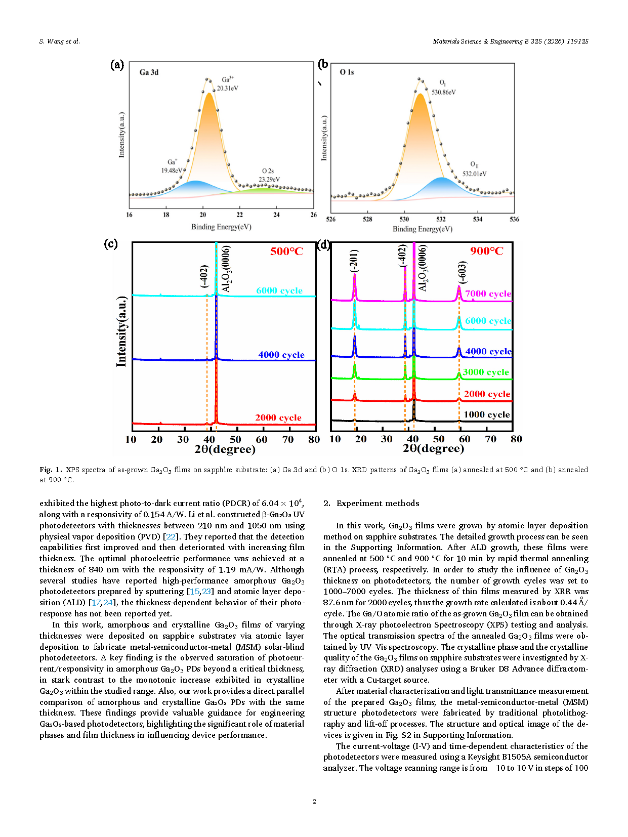
Fig. 2. The (αhν)2 versus hν spectrum of Ga2O3 films with different thickness annealed at (a) 500 ◦C (b) 900 ◦C; Extracted Urbach energy Eu of Ga2O3 films annealed at (c) 500 ◦C (d) 900 ◦C.
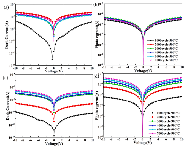
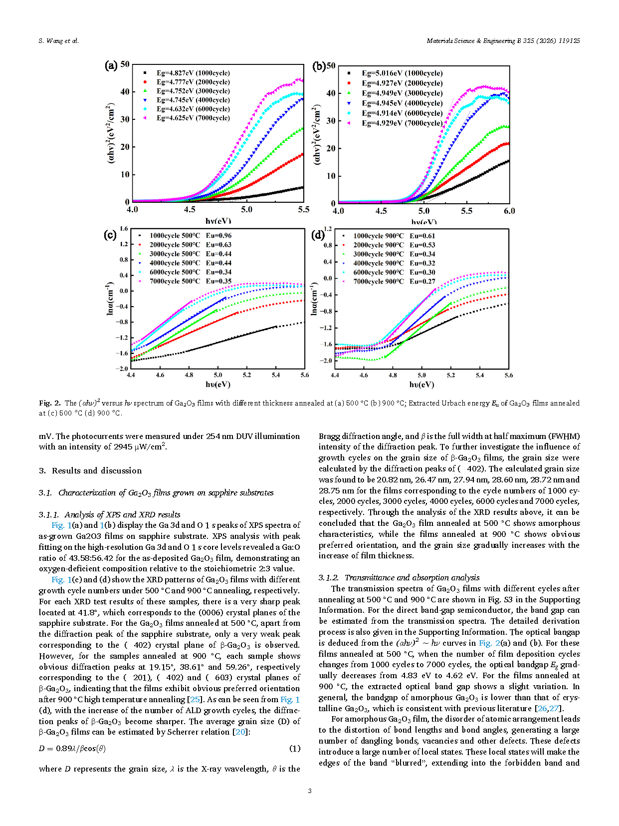
Fig. 3. The I–V curves of amorphous Ga2O3 PDs for different cycles (a) in the dark and (b) under 254 nm illumination; The I–V curves of crystalline Ga2O3 PDs for different cycles (c) in the dark and (d) under 254 nm illumination.
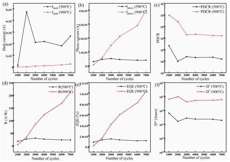
Fig. 4. Comparison of different parameters versus ALD cycle number for amorphous (500 ◦C) and crystalline (900 ◦C) Ga2O3 photodetectors. (a) dark current (b) photo current (c) PDCR (d) responsivity (e) external quantum efficienc and (f) specific detectivity.
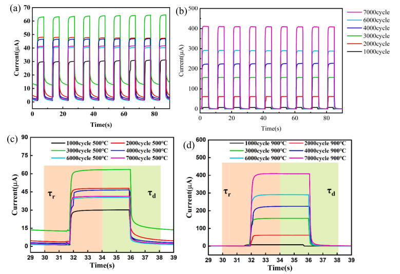
Fig. 5. The multi-cycle time-dependent photoresponse characteristics of samples annealed at (a) 500 ◦C and (b) 900 ◦C; The partial enlargement of the photoresponse curves for different cycles annealed at (c) 500 ◦C and (d) 900 ◦C at 10 V bias.
DOI:
doi.org/10.1016/j.mseb.2025.119125