Paper Sharing
【Member Papers】Research on β-Ga₂O₃ Photoconductive Assisted Switch
日期:2026-01-06阅读:503
Researchers from the JFS Laboratory, Beijing Huairou Laboratory and Huazhong University of Science and Technology have published a dissertation titled "Research on β-Ga2O3 Photoconductive Assisted Switch" in 2025 22nd China International Forum on Solid State Lighting & 2025 11th International Forum on Wide Bandgap Semiconductors (SSLCHINA: IFWS).
Background
Gallium Oxide (Ga2O3) has been given great attention for future power electronic systems in recent years due to its 4.8 eV bandgap induced ∼ 8MV/cm critical field, decent simulated intrinsic electron mobility of 250 cm2 /Vs, high simulated saturation velocity of 2.0 × 107 cm/s, as well as the controllable n-type doping concentration. In addition to these outstanding material properties, and its bulk single crystals can be fabricated by several cost-effective methods with high-quality and large diameter. This makes the βGa2O3 to be very attractive for future commercialization.
One of the main challenges that hinder the development of Ga2O3 device technology is the p-type issue. And the absence of p-type β-Ga2O3 has been limiting the design of β-Ga2O3-based bipolar devices, which possesses low leakage current, high thermal stability, and good surge handling capability. Due to the lack of p-type doping, the academic community has been gradually focusing on the research of unipolar devices such as Schottky barrier diodes (SBDs) and metal oxide semiconductor field effect transistors (MOSFETs). Although a large number of studies have been demonstrated that the use of β-Ga2O3 heterojunctions can make up for the absence of p-type doping, it is still unable to completely replace p-type gallium oxide in bipolar device design due to the problem of heterojunction interface, which will result in the excellent material properties of Ga2O3 could not be fully shown. So, what structure can play the excellent characteristics of Ga2O3 without the need for p-type gallium oxide? a new concept of photoconductive assisted switch (PCAS) based on β-Ga2O3 is proposed, which is different from the traditional photoconductive semiconductor switch (PCCS).
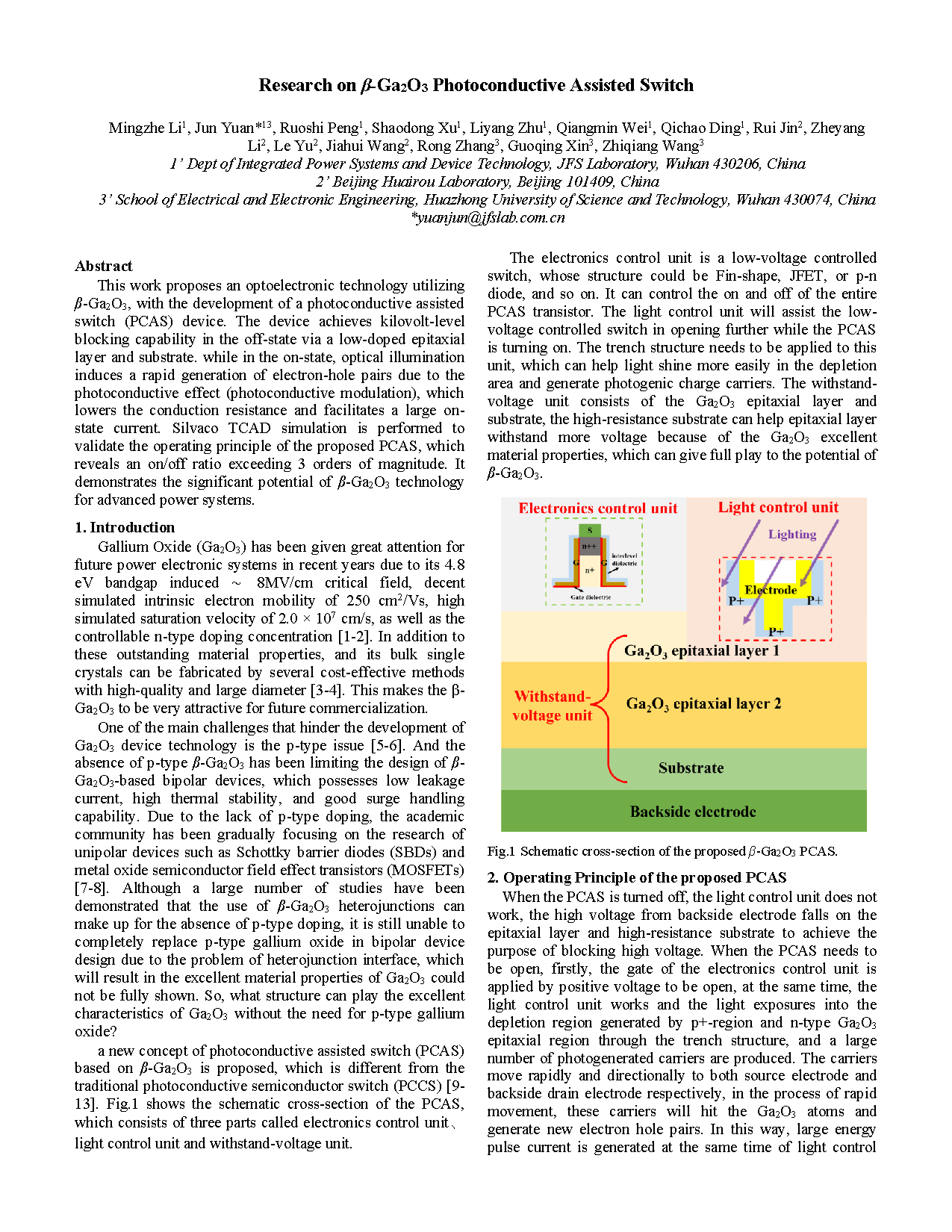
The electronics control unit is a low-voltage controlled switch, whose structure could be Fin-shape, JFET, or p-n diode, and so on. It can control the on and off of the entire PCAS transistor. The light control unit will assist the low-voltage controlled switch in opening further while the PCAS is turning on. The trench structure needs to be applied to this unit, which can help light shine more easily in the depletion area and generate photogenic charge carriers. The withstand-voltage unit consists of the Ga2O3 epitaxial layer and substrate, the high-resistance substrate can help epitaxial layer withstand more voltage because of the Ga2O3 excellent material properties, which can give full play to the potential of β-Ga2O3.
Abstract
This work proposes an optoelectronic technology utilizing β-Ga2O3, with the development of a photoconductive assisted switch (PCAS) device. The device achieves kilovolt-level blocking capability in the off-state via a low-doped epitaxial layer and substrate. while in the on-state, optical illumination induces a rapid generation of electron-hole pairs due to the photoconductive effect (photoconductive modulation), which lowers the conduction resistance and facilitates a large onstate current. Silvaco TCAD simulation is performed to validate the operating principle of the proposed PCAS, which reveals an on/off ratio exceeding 3 orders of magnitude. It demonstrates the significant potential of β-Ga2O3 technology for advanced power systems.
Conclusion
In summary, this work proposes an optoelectronic integration technology utilizing β-Ga2O3, with the development of a photoconductive assisted switch (PCAS) device. The device achieves kilovolt-level blocking capability in the off-state via a low-doped epitaxial layer and substrate; while in the on-state, optical illumination induces a rapid generation of electron-hole pairs due to the photoconductive effect (photoconductive modulation), which lowers the conduction resistance and facilitates a large on-state current. Simulation results from Silvaco attest to the operational principle and feasibility of the proposed PCAS, which demonstrates the significant potential of β-Ga2O3 technology for advanced power systems.
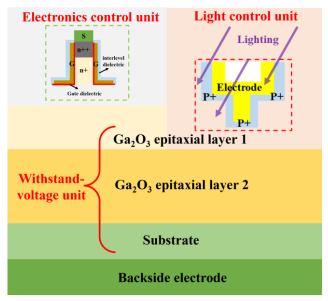
Fig.1 Schematic cross-section of the proposed β-Ga2O3 PCAS.

Fig.2 Equivalent schematic diagram of the proposed β-Ga2O3 PCAS.
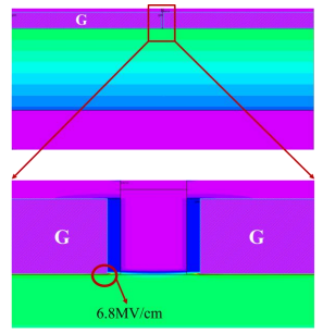
Fig.3 E-field distribution at 650V of the FinFET in the off-state.
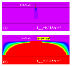
Fig.4 Silvaco TCAD simulation of the PCAS of the FinFET. (a) Off-current density in the dark. (b) On-current density with an illumination intensity of 1W/cm2.
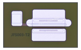
Fig.5 Optical image of the β-Ga2O3 MOSFET.
DOI:
doi.org/10.1109/SSLCHINAIFWS69008.2025.11315036