Paper Sharing
【International Papers】Exploiting Mg-Interdiffusion-Driven Work-Function Reduction in Ti/Mg/Ti Multilayers to Achieve Low-Resistivity Ohmic Contacts to (001) β-Ga₂O₃
日期:2026-01-07阅读:493
Researchers from the Sejong University have published a dissertation titled " Exploiting Mg-Interdiffusion-Driven Work-Function Reduction in Ti/Mg/Ti Multilayers to Achieve Low-Resistivity Ohmic Contacts to (001) β-Ga2O3" in ACS Nano.
Background
β-Gallium oxide (β-Ga2O3) is an ultrawide bandgap semiconductor with a bandgap of ∼4.8 eV, which is greater than that of silicon (Si), silicon carbide (SiC), and gallium nitride (GaN). A merit of this ultrawide bandgap is the high critical electric field for breakdown, which is theoretically estimated to be 8 MV/cm in β-Ga2O3. This allows for a superior Baliga’s figure-of-merit of β-Ga2O3-based power device, i.e., they potentially can achieve a smaller on-resistance as compared to the Si, SiC, and GaN-based power devices with the identical breakdown voltage. Furthermore, the possibility of large-diameter wafers with low cost also makes β-Ga2O3 a promising candidate for next-generation power semiconductors.
Abstract
Low-resistivity Ohmic contact formation in β-gallium oxide (β-Ga2O3) is crucial for high-efficiency power electronics and deep-ultraviolet (DUV) optoelectronic devices. In this study, we successfully developed a Ti/Mg/Ti multilayered metal stack (20 nm/50 nm/20 nm) as an Ohmic contact to (001) β-Ga2O3. The Mg interlayer, with its low work function relative to Ti and the electron affinity of β-Ga2O3, effectively reduces the Schottky barrier, enabling low contact resistivity. The Ti layers on both sides of the Mg layer act as protective caps, preventing Mg oxidation and improving chemical stability. Ultraviolet photoelectron spectroscopy (UPS) analysis showed that the Ti/Mg/Ti metal stack achieved a stabilized work function of ∼3.94 eV after 400 °C annealing, close to β-Ga2O3’s electron affinity, facilitating efficient electron injection. X-ray photoelectron spectroscopy (XPS) confirmed interfacial stability, indicating that the stack protects the reactive Mg layer while compensating for the higher work function of Ti. Moreover, cross-sectional transmission electron microscopy and elemental mapping analysis reveal that the in situ formed interfacial TiOx layer on (001) β-Ga2O3 is relatively thin (2.5 nm) and homogeneous. Importantly, Mg diffusion into Ti layers highly affects the reduction of the effective work function. Transmission electron microscopy and elemental analysis further confirm that Mg diffuses into the Ti layers, leading to the formation of a Ti–Mg alloy. This alloying effect significantly reduces the effective work function of the contact, thereby facilitating electron injection and lowering the contact resistance. Transmission line model (TLM) measurements revealed a contact resistivity of 6.25 × 10⁻⁴ Ω·cm2 for the 400 °C annealed Ti/Mg/Ti metal stack, which is significantly lower than that of Ti or Mg alone. Moreover, TLM measurements performed under cryogenic temperatures revealed that the Ti/Mg/Ti contact stack annealed at 400 °C in an argon (Ar) atmosphere exhibits minimal temperature dependence, indicating that carrier transport is predominantly governed by tunneling. A similar tunneling-dominated behavior was also observed for samples annealed in vacuum and nitrogen (N2) atmospheres. In contrast, contacts annealed in air showed a strong temperature dependence, confirming that thermionic emission is the dominant transport mechanism in this case. These electrical observations are fully supported by XPS analysis, which shows significant oxidation of both Mg and Ti for the air-annealed samples, reduced oxidation for N2 and vacuum annealing, and the lowest oxidation level for Ar annealing. The reduced oxidation in inert and oxygen-free environments enhances tunneling, whereas the high oxide formation in air suppresses tunneling and strengthens thermionic emission. Overall, the combined TLM and XPS results clearly demonstrate that the annealing atmosphere plays a critical role in defining the contact transport mechanism, with Ar providing the most stable and tunneling-favorable interface. Finally, the proposed metal stack-based Ohmic contact (Ti/Mg/Ti contact stack annealed at 400 °C in an Ar atmosphere) was incorporated into β-Ga2O3-based metal–semiconductor–metal (MSM) photodetectors to assess device performance. Under 2 μW of 255 nm DUV illumination, the devices exhibited a high responsivity of 14,240.7 A/W. These findings demonstrate that the Ti/Mg/Ti multilayer approach effectively combines low work function engineering with oxidation protection to achieve low-resistance, chemically stable Ohmic contacts. This strategy offers a promising route for enhancing β-Ga2O3-based high-power and DUV optoelectronic devices.
Conclusions
In this study, we proposed and demonstrated a novel Ti/Mg/Ti multilayered metal stack to significantly enhance the not only Ohmic behavior but also optoelectronic performance of β-Ga2O3-based devices. Through a combination of UPS, XPS, and TLM analyses, the Ti/Mg/Ti multilayered metal stack was shown to effectively address the two key challenges associated with conventional metal contacts: the high work function of Ti compared to the electron affinity of β-Ga2O3 and the extreme surface reactivity of Mg. First, UPS analysis confirmed that the Ti/Mg/Ti multilayered metal stack annealed at 400 °C exhibited a low effective work function of ∼3.94 eV closely matching the electron affinity of β-Ga2O3 thus promoting near zero or even negative SBH. Moreover, this result was supported by the theoretical model of thickness-weighted averaging of work functions in stacked metals. Second, XPS analysis revealed that the multilayered stack suppresses excessive surface oxidation of Mg by encapsulating it with Ti layers, which form a passivating TiOx layer and maintain interfacial integrity. Furthermore, depth profile analyses confirmed limited interdiffusion and formation of beneficial interfacial compounds such as Ti−Ga and Ti−Mg, which may further enhance electrical connectivity. TEM analysis confirmed Mg diffusion and the formation of an interfacial layer. Mg was observed to diffuse on both sides of the Ti layers, with a higher concentration in the top layer. This difference is attributed to the structural contrast between the polycrystalline top layer deposited on Mg and the monocrystalline (001) β-Ga2O3 substrate beneath the bottom layer. Moreover, TLM measurements showed that the Ti/Mg/Ti multilayered metal stack annealed at 400 °C exhibited a remarkably low specific ρc of 6.25 × 10⁻⁴ Ω·cm2, outperforming conventional approaches. It is noted that, annealing at temperatures exceeding 400 °C (i.e., 600−800 °C) resulted in degradation in electrical performance due to increased oxidation and interfacial disorder. This result emphasizes the importance of carefully optimizing annealing conditions to balance work function reduction and thermal stability. TLM measurements conducted at cryogenic temperatures clearly show that the Ohmic contacts Ti/Mg/Ti multilayered metal stack annealed at 400 °C in an Ar atmosphere exhibit the weakest temperature dependence, indicating a tunneling-dominated transport mechanism. Similar behavior is observed for contacts annealed in vacuum and N2 atmospheres. In contrast, air-annealed contacts display a strong temperature dependence, confirming that thermionic emission dominates under oxidizing conditions. These electrical findings are fully supported by XPS analysis, which reveals severe oxidation of Mg and Ti in air-annealed samples, reduced oxidation in N2 and vacuum conditions, and minimal oxidation in Ar condition. Reduced interfacial oxidation in inert atmospheres promotes tunneling, whereas oxide formation in air suppresses tunneling and enhances thermionic emission. Finally, in order to validate the practical advantages of this proposed approach, the Ti/Mg/Ti multilayered metal stack was employed to Ohmic contacts of β-Ga2O3 MSM photodetectors. As a result, under 255 nm illumination and − 10 V bias, the MSM photodetectors demonstrated exceptional optoelectronic performance, including Iph exceeding 51 mA and R reaching up to 14,240.7 A/W at 2 μW of incident power. D* also reached as high as 1.67 × 10¹¹ Jones. These outstanding figures of merit confirm the critical role of optimized Ohmic contact in enhancing photodetector performance by minimizing voltage drops, enabling high internal gain, and reducing power consumption. Overall, this work firmly establishes the Ti/Mg/ Ti multilayered metal stack as a promising candidate for achieving low-resistance, thermally stable, and chemically robust Ohmic contacts to β-Ga2O3-based devices. In other words, this approach offers a practical and scalable solution for realizing high-performance DUV optoelectronic devices suited for demanding applications such as flame detection, environmental monitoring, DUV imaging, and space-based DUV sensing systems. As part of our future work, we intend to further investigate the applicability of the Ti/Mg/Ti multilayered metal stack in advanced device architectures. In particular, we aim to demonstrate its effectiveness in β-Ga2O3 metal-oxide-semiconductor field-effect transistors (MOSFETs) to evaluate contact resistance and thermal stability, as well as in fin fieldeffect transistor (FinFET) structures to assess scalability and interface uniformity. This study will help validate the versatility of the proposed Ohmic contact design across various β-Ga2O3 based device platforms.
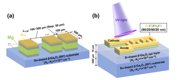
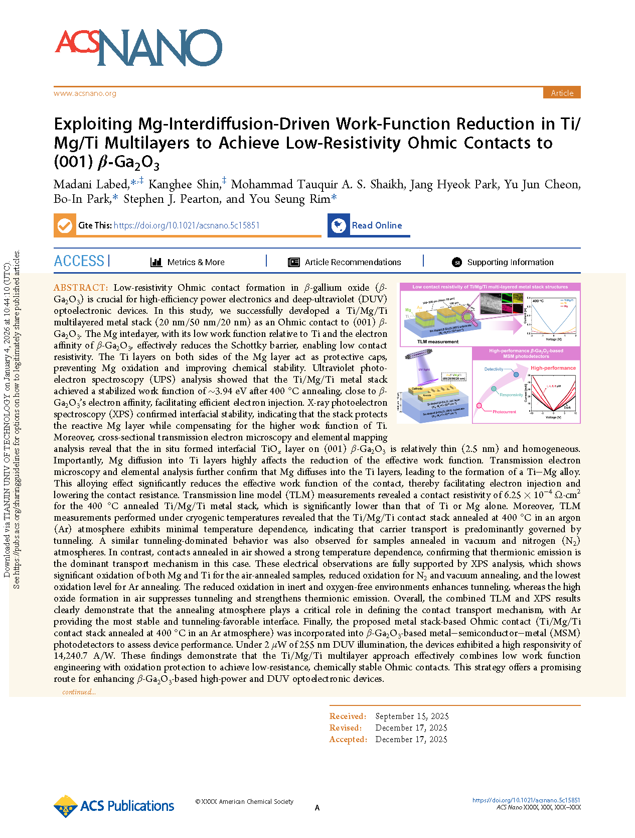
Figure 1. 3D schematic of (a) pattern for TLM measurement and (b) β-Ga2O3-based MSM photodetector utilizing Ti/Mg/Ti multilayered metal stack.
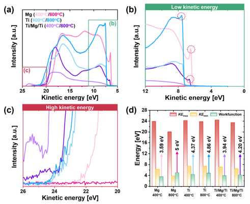
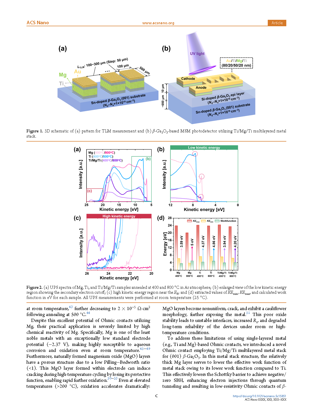
Figure 2. (a) UPS spectra of Mg, Ti, and Ti/Mg/Ti samples annealed at 400 and 800 °C in Ar atmosphere; (b) enlarged view of the low kinetic energy region showing the secondary electron cutoff; (c) high kinetic energy region near the EF; and (d) extracted values of KEmin, KEmax, and calculated work function in eV for each sample. All UPS measurements were performed at room temperature (25 °C).
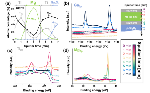
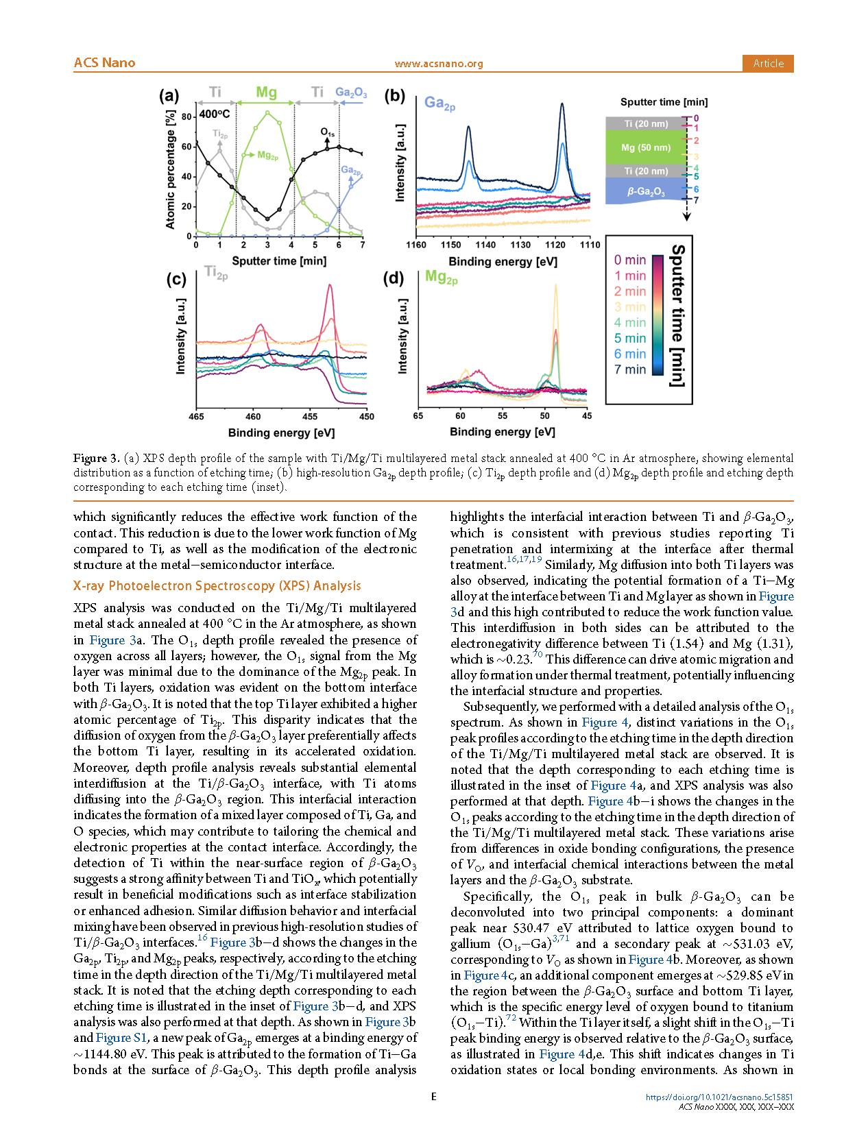
Figure 3. (a) XPS depth profile of the sample with Ti/Mg/Ti multilayered metal stack annealed at 400 °C in Ar atmosphere, showing elemental distribution as a function of etching time; (b) high-resolution Ga2p depth profile; (c) Ti2p depth profile and (d) Mg2p depth profile and etching depth corresponding to each etching time (inset).
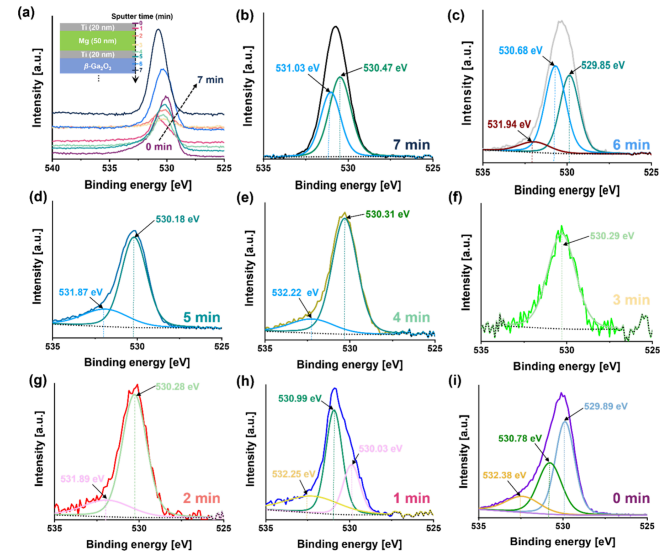
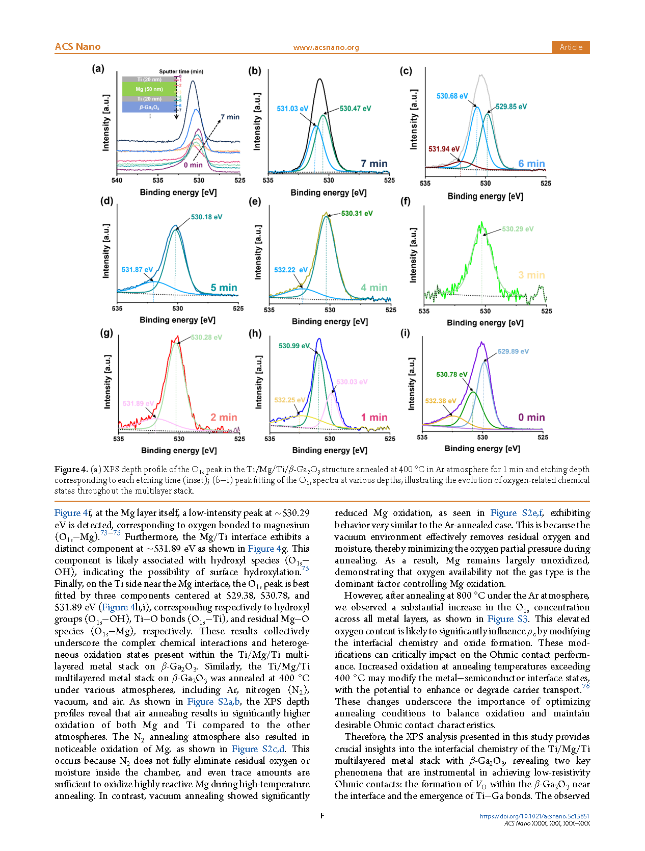
Figure 4. (a) XPS depth profile of the O1s peak in the Ti/Mg/Ti/β-Ga2O3 structure annealed at 400 °C in Ar atmosphere for 1 min and etching depth corresponding to each etching time (inset); (b−i) peak fitting of the O1s spectra at various depths, illustrating the evolution of oxygen-related chemical states throughout the multilayer stack.
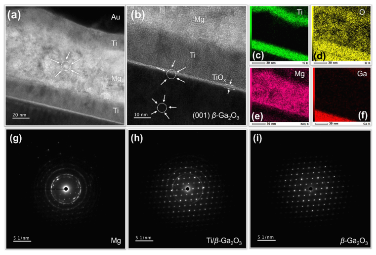
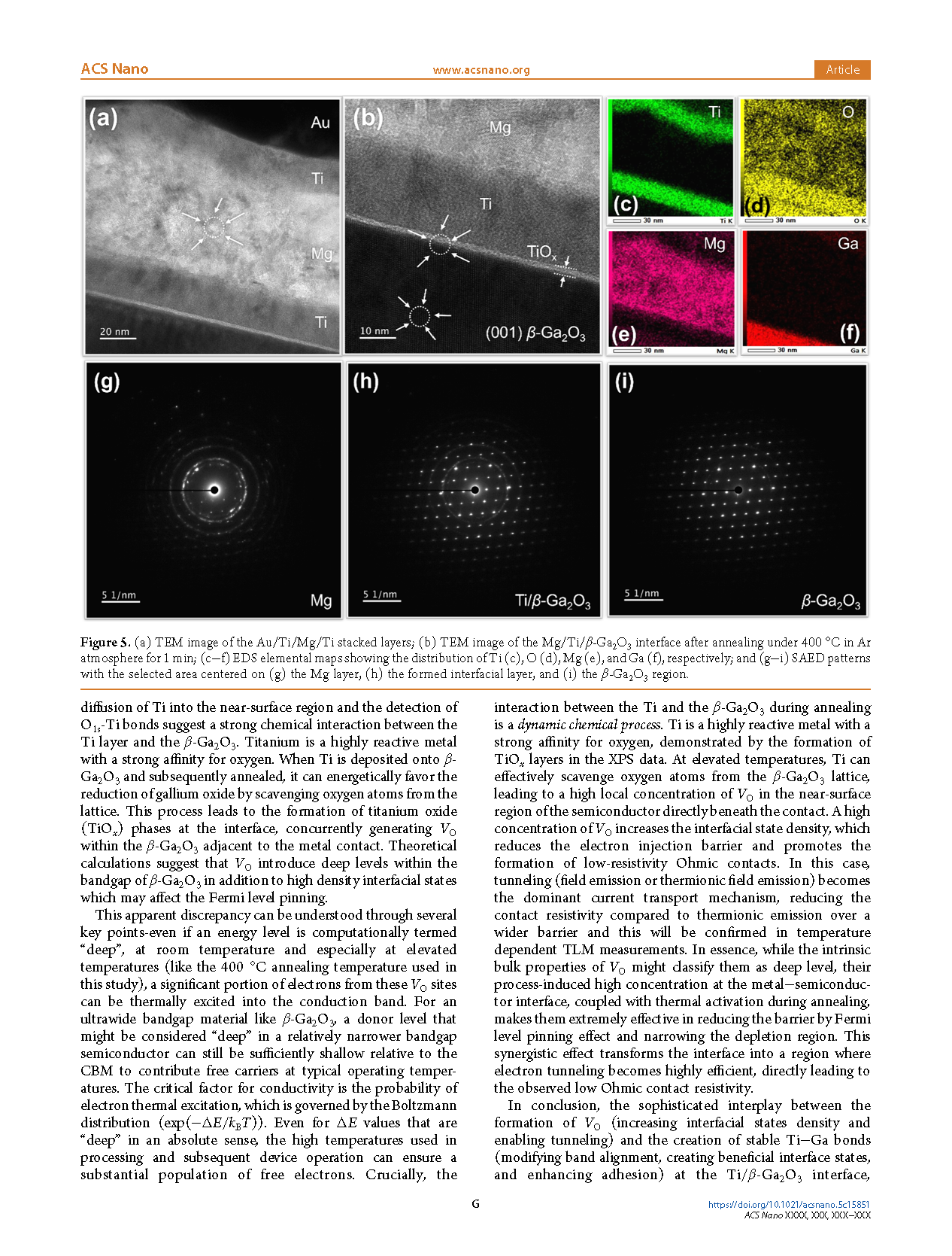
Figure 5. (a) TEM image of the Au/Ti/Mg/Ti stacked layers; (b) TEM image of the Mg/Ti/β-Ga2O3 interface after annealing under 400 °C in Ar atmosphere for 1 min; (c−f) EDS elemental maps showing the distribution of Ti (c), O (d), Mg (e), and Ga (f), respectively; and (g−i) SAED patterns with the selected area centered on (g) the Mg layer, (h) the formed interfacial layer, and (i) the β-Ga2O3 region.
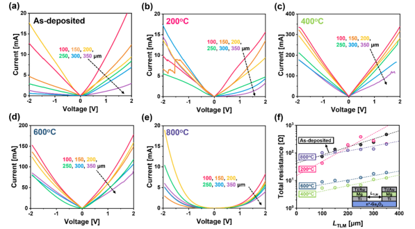
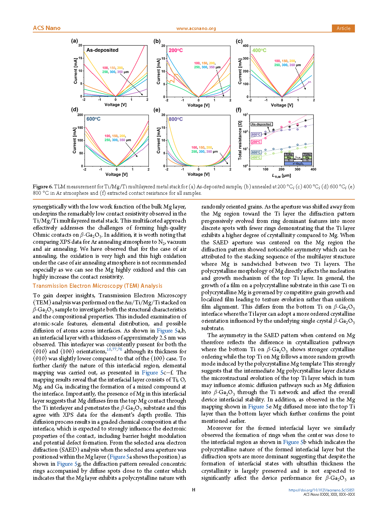
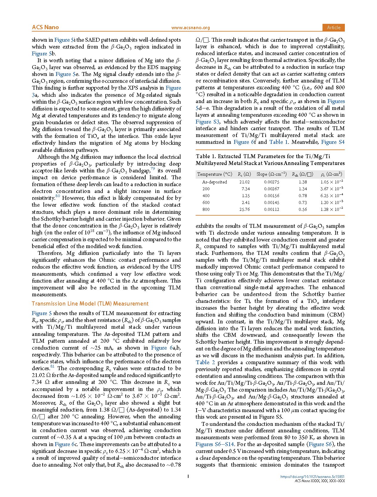
Figure 6. TLM measurement for Ti/Mg/Ti multilayered metalstack for (a) As-deposited sample; (b) annealed at 200 °C; (c) 400 °C; (d) 600 °C; (e) 800 °C in Ar atmosphere and (f) extracted contact resistance for all samples.
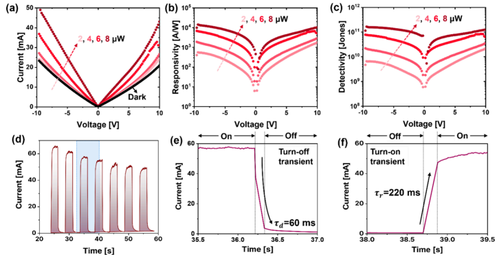
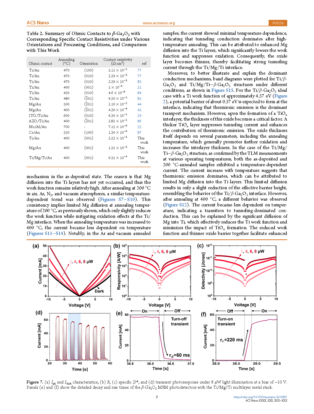
Figure 7. (a) Iph and Idark characteristics, (b) R, (c) specific D*, and (d) transient photoresponse under 8 μW light illumination at a bias of −10 V. Panels (e) and (f) show the detailed decay and rise times of the β-Ga2O3 MSM photodetectors with the Ti/Mg/Ti multilayer metal stack.
DOI:
doi.org/10.1021/acsnano.5c15851