Paper Sharing
【Domestic Papers】a-SnOₓ/β-Ga₂O₃ Junction Field-effect Phototransistor with High Responsivity and Fast Response Speed
日期:2026-01-07阅读:406
Researchers from the University of Science and Technology of China have published a dissertation titled "a-SnOx/β-Ga2O3 Junction Field-effect Phototransistor with High Responsivity and Fast Response Speed" in 2025 22nd China International Forum on Solid State Lighting & 2025 11th International Forum on Wide Bandgap Semiconductors (SSLCHINA: IFWS).
Project Support
This work was supported in part by the National Key Research and Development Program of China under Grant 2024YFA1208800 and Grant 2023YFB3610200, in part by the National Natural Science Foundation of China under Grant 62304215 and Grant 62171426, in part by the University of Science and Technology of China (USTC) under Grant WK2100000056, and in part by the Center for Micro and Nanoscale Research and Fabrication of USTC.
Background
In recent years, wide-bandgap semiconductor materials are considered ideal candidates for high-performance solar-blind UV photodetectors (SBPDs) due to their outstanding radiation resistance, excellent thermal and chemical stability, and strong absorption in the deep UV region. Among the various wide-bandgap semiconductors, β-Ga2O3 stands out with an intrinsic bandgap of approximately 4.9 eV. This wide bandgap corresponds to an absorption cutoff wavelength below 280 nm, thereby nearly covering the entire solar-blind UV spectrum. In addition to its spectral advantages, β-Ga2O3 exhibits remarkable thermal stability and is recognized as the most thermodynamically stable phase among its polymorphs. Moreover, its naturally cleavable (100) crystal plane offers favorable conditions for the fabrication of low-dimensional nanostructures. The β-Ga2O3 has demonstrated enhanced photoresponse characteristics through its integration into various types of photoelectronic devices, including two-terminal devices (such as Schottky and PN diodes and three-terminal devices (such as metal-oxide-semiconductor field-effect transistors and junction field-effect transistors). However, two-terminal devices generally suffer from limited photoconductive gain, insufficient noise suppression, and restricted response speed, and they lack the ability to dynamically modulate the channel current via gate control, which constrains their application in high-performance UV detection.
Abstract
Gallium oxide (Ga2O3) is known for its exceptional properties, making it an ideal material for solar-blind photodetectors. This study demonstrates a high-performance solar-blind UV phototransistor based on amorphous (a-) SnOx(1<x<2)/β−Ga2O3 nanosheet heterojunction field-effect transistor. It exhibits excellent optoelectronic properties under 254 nm illumination, with ultra-high responsivity (1.16×10⁴ A/W) at weak light intensity. With increasing UV illumination, the device demonstrates an ultrafast response, achieving rise times as low as 487 μs. The excellent performance originates from the strong interfacial built-in field enabling efficient carrier separation and suppressed recombination, photogating from trapped charges in SnOx, and transistor transconductance amplification. The device provides a promising approach for solar-blind photodetection.
Conclusions
In summary, by employing a a-SnOx/β-Ga2O3 JFEPT structure and optimizing the SnOx layer via N2 annealing, we achieve a high-performance SBPD. This device delivers an outstanding responsivity of 1.16 × 10⁴ A/Wunder UV illumination (1.766 µW/cm2), along with a high PDCR of 1.03 × 10⁶. With increasing UV illumination, it retains rapid rise time of 487 µs. Overall, this work provides a promising strategy for designing and optimizing next- generation Ga2O3-based SBPDs.
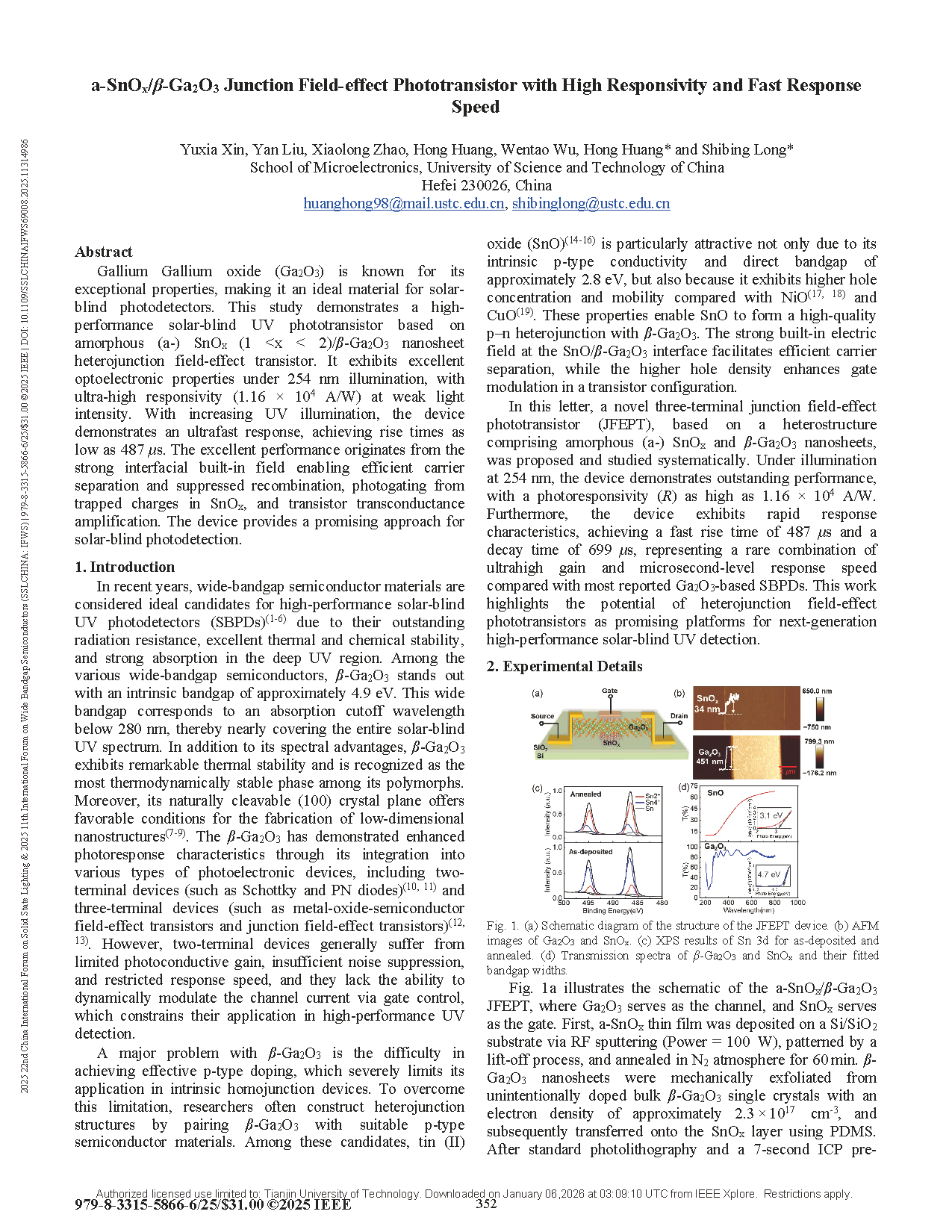
Fig. 1. (a) Schematic diagram of the structure of the JFEPT device. (b) AFM images of Ga2O3 and SnOx. (c) XPS results of Sn 3d for as-deposited and annealed. (d) Transmission spectra of β-Ga2O3 and SnOx and their fitted bandgap widths.
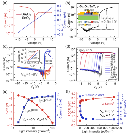
Fig. 2. (a) I-V curve of Ga2O3 nanosheets (red curve) and Ohmic characteristics of SnOx with Ni/Au electrodes (Blue curve). (b) Rectifying I– V curve of the SnOx/Ga2O3 PN junction. (c) Transfer curves (Vds from 1 V to 9 V) of the a-SnOx/β-Ga2O3 JFEPT in the dark. The inset shows the double- sweep transfer curve. (d) Transfer curves of the a-SnOx/β-Ga2O3 JFEPT under dark and 254 nm light illumination with different intensities. (e) Threshold voltage shift (ΔVth) with light intensity and the relationship between the photocurrent and light intensity at Vg = − 3V. (f) PDCR and R of the JFEPT as a function of light intensity.
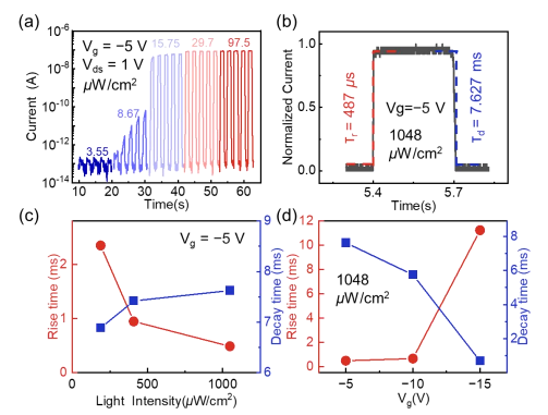
Fig. 3. (a) I-t curves of the a-SnOx/β-Ga2O3 JFEPT under different light intensities (Vg = −5 V, Vds = 1 V). (b) A magnified image of the I–t curve of the JFEPT device at Vg = −5 V and 1048 μW/cm2 illumination (captured by an oscilloscope). (c) Response time of the device as a function of light intensities. (d) Response time of the device as a function of gate voltages.
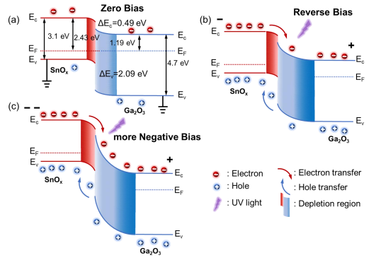
Fig. 4. (a) Schematic of the energy band diagrams of Ga2O3/SnOx heterojunction. (b) Schematics of the carrier transport mechanism under UV illumination with a negative gate bias applied. (c) Energy band diagram under UV illumination with a more negative gate bias applied.
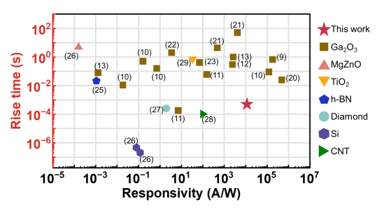
Fig. 5. Comparison of the responsivity and response speed of the a-SnOx/β-Ga2O3 JFEPT with other reported photodetectors.
DOI:
doi.org/10.1109/SSLCHINAIFWS69008.2025.11314986