Paper Sharing
【Member Papers】Recent Advances in Ohmic Contact with β-Ga₂O₃: A Review
日期:2026-01-09阅读:456
Researchers from the Fudan University have published a dissertation titled "Recent Advances in Ohmic Contact with β-Ga2O3: A Review" in 2025 22nd China International Forum on Solid State Lighting & 2025 11th International Forum on Wide Bandgap Semiconductors (SSLCHINA: IFWS).
Project Support
This work is supported by the National Key R&D Program of China (2023YFB4606300), the National Natural Science Foundation of China (62474049), the Science and Technology Innovation Plan of Shanghai Science and Technology Commission (No.21DZ110080,23ZR1405300) and the Joint Research Plan of sci-tech innovation communityin Yangtze River Delta (No. 2023CSJG0600).
Background
β-Ga₂O₃ (gallium oxide) is regarded as a promising material for next-generation high-power electronic devices and solar-blind ultraviolet photodetectors. With an ultra-wide bandgap of approximately 4.8 eV, a theoretical breakdown electric field as high as 8 MV/cm, and a Baliga figure of merit (BFOM) of 3334, β-Ga₂O₃ offers outstanding intrinsic advantages. At the same breakdown voltage, its on-state conduction loss is theoretically one order of magnitude lower than that of silicon carbide (SiC) and gallium nitride (GaN) devices, and it also benefits from relatively mature and controllable n-type doping technologies.
However, the formation of low-resistance ohmic contacts remains a critical bottleneck preventing β-Ga₂O₃ devices from achieving their expected performance. Owing to its extremely wide bandgap and the presence of a high density of intrinsic and extrinsic defects as well as surface states, severe Fermi-level pinning occurs at the surface of β-Ga₂O₃. As a result, contact with most metals leads to the formation of high Schottky barrier heights, making efficient current injection and low-resistance ohmic contacts particularly difficult to realize.
Abstract
β-Gallium Oxide (Ga2O3) is considered a potential material for next-generation high-power electronics and optoelectronic devices due to its ultra-wide bandgap (∼4.8eV) and high breakdown voltage (8MV/cm). It exhibits great promise for high-voltage, high-power, and low-loss power electronics devices. However, the performance of Ga2O3 based devices remains far from expectations, with a considerable gap existing before large-scale industrialization can be achieved. One of the key challenges hindering the development of β−Ga2O3 materials and devices is the formation of metal /β - Ga2O3 contacts. Compared to other semiconductors, the extremely wide bandgap of β−Ga2O3 makes it more challenging to achieve ohmic contacts. Therefore, an in-depth investigation into the physical mechanism underlying the metal /β−Ga2O3 contact interface is crucial for enhancing device performance and facilitating its practical application. One of the key criteria for the successful preparation of β−Ga2O3 power devices is the formation of ohmic contacts with low specific contact resistivity and high reliability. In this work, recent advances in ohmic contact with β−Ga2O3 have been reviewed. Initially, we provided a concise overview of prior research advancements concerning the ohmic contact formation of β−Ga2O3. This includes the utilization of conventional Ti/Au electrodes as well as the application of processes such as rapid thermal annealing (RTA) and reactive ion etching (RIE) to achieve ohmic contacts in β−Ga2O3. Subsequently, we present a detailed discussion of recent developments in ohmic contact with β-Ga2O3, focusing on β-Ga2O3 ohmic contact preparation from four perspectives: annealing technique, surface treatment method, multilayer electrode, and ion implantation strategy. This paper not only offers novel insights into the selection of ohmic contact electrode materials and fabrication processes for β-Ga2O3, but also elucidates the reaction mechanisms at the metal/β-Ga2O3 interface and the underlying physical principles involved in the formation of ohmic contacts. Furthermore, it contributes to a deeper understanding of the developmental trends in β-Ga2O3 ohmic contact strategies.
Conclusion
This review has systematically consolidated recent critical advances in overcoming the primary challenge of forming low ρc ohmic contacts to β-Ga2O3 by exploring four strategic pathways, innovative annealing techniques, advanced surface treatments, multilayer electrode design, and ion implantation. It is significant that achieving low ρc relies on the deliberate engineering of the metal/β-Ga2O3 interface. Beyond synthesizing these findings, this work provides a valuable framework for guiding both fundamental research and practical device fabrication. This comprehensive understanding marks a significant step toward the realization of high-performance β-Ga2O3-based power electronics.
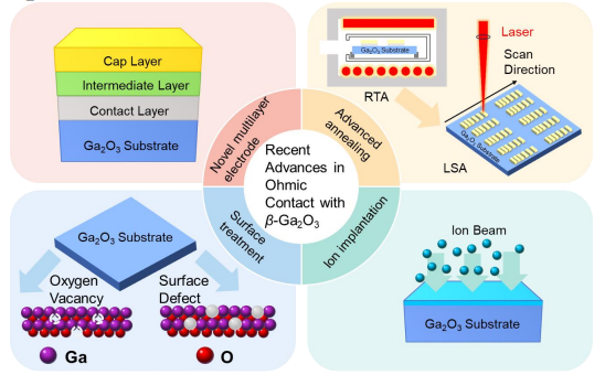
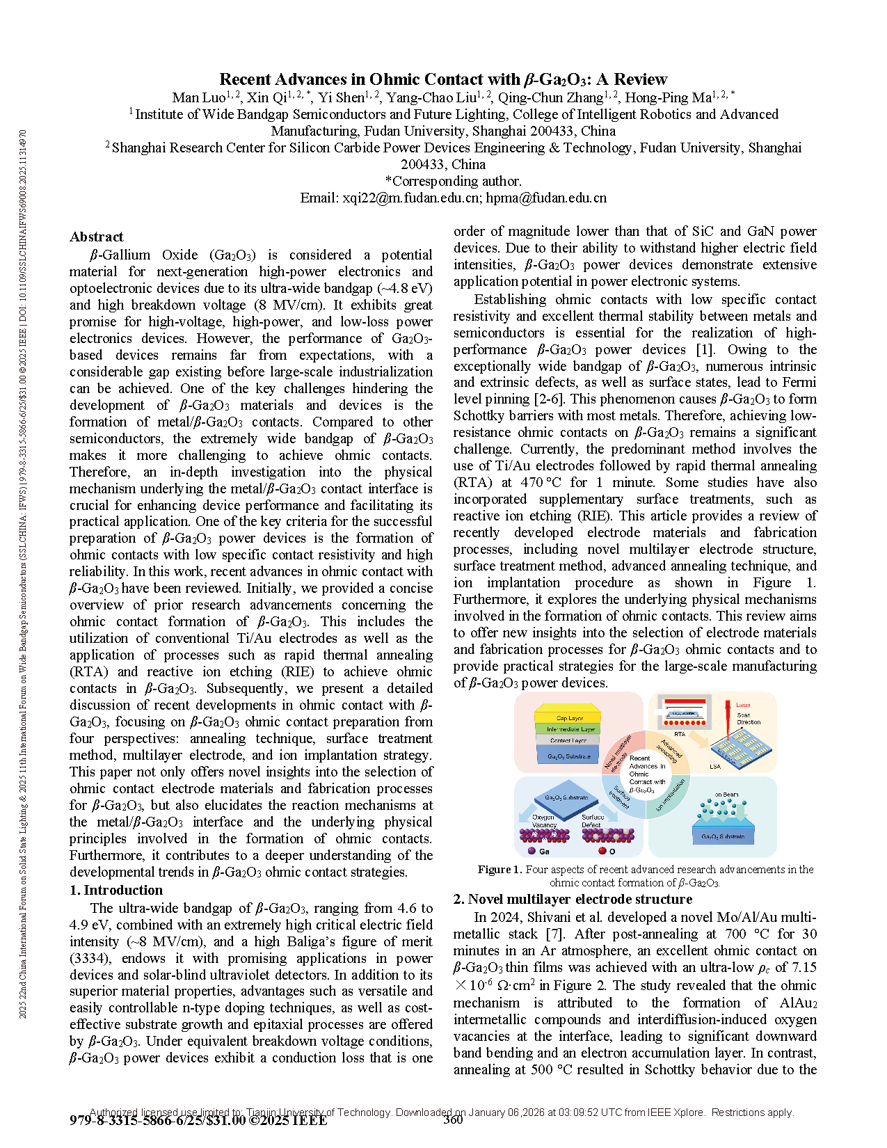
Figure 1. Four aspects of recent advanced research advancements in the ohmic contact formation of β-Ga2O3.
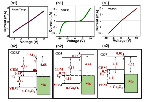
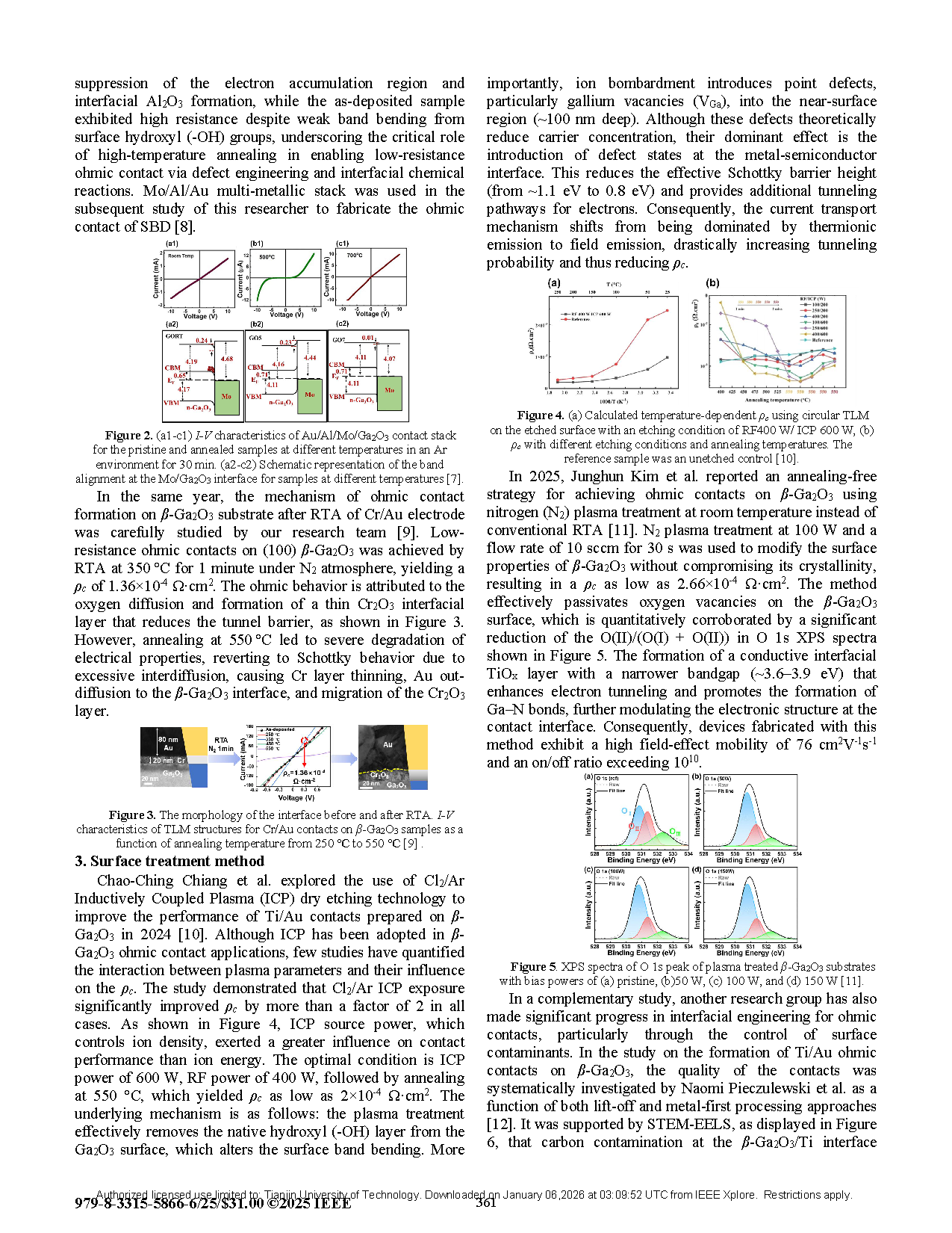
Figure 2. (a1-c1) I-V characteristics of Au/Al/Mo/Ga2O3 contact stack for the pristine and annealed samples at different temperatures in an Ar environment for 30 min. (a2-c2) Schematic representation of the band alignment at the Mo/Ga2O3 interface for samples at different temperatures [7].
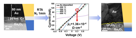
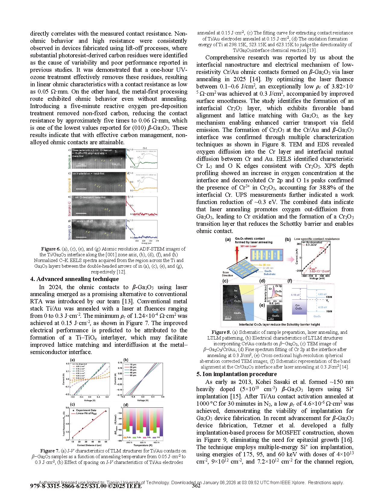
Figure 3. The morphology of the interface before and after RTA. I-V characteristics of TLM structures for Cr/Au contacts on β-Ga2O3 samples as a function of annealing temperature from 250 ℃ to 550 ℃ [9].
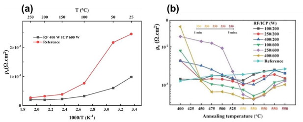
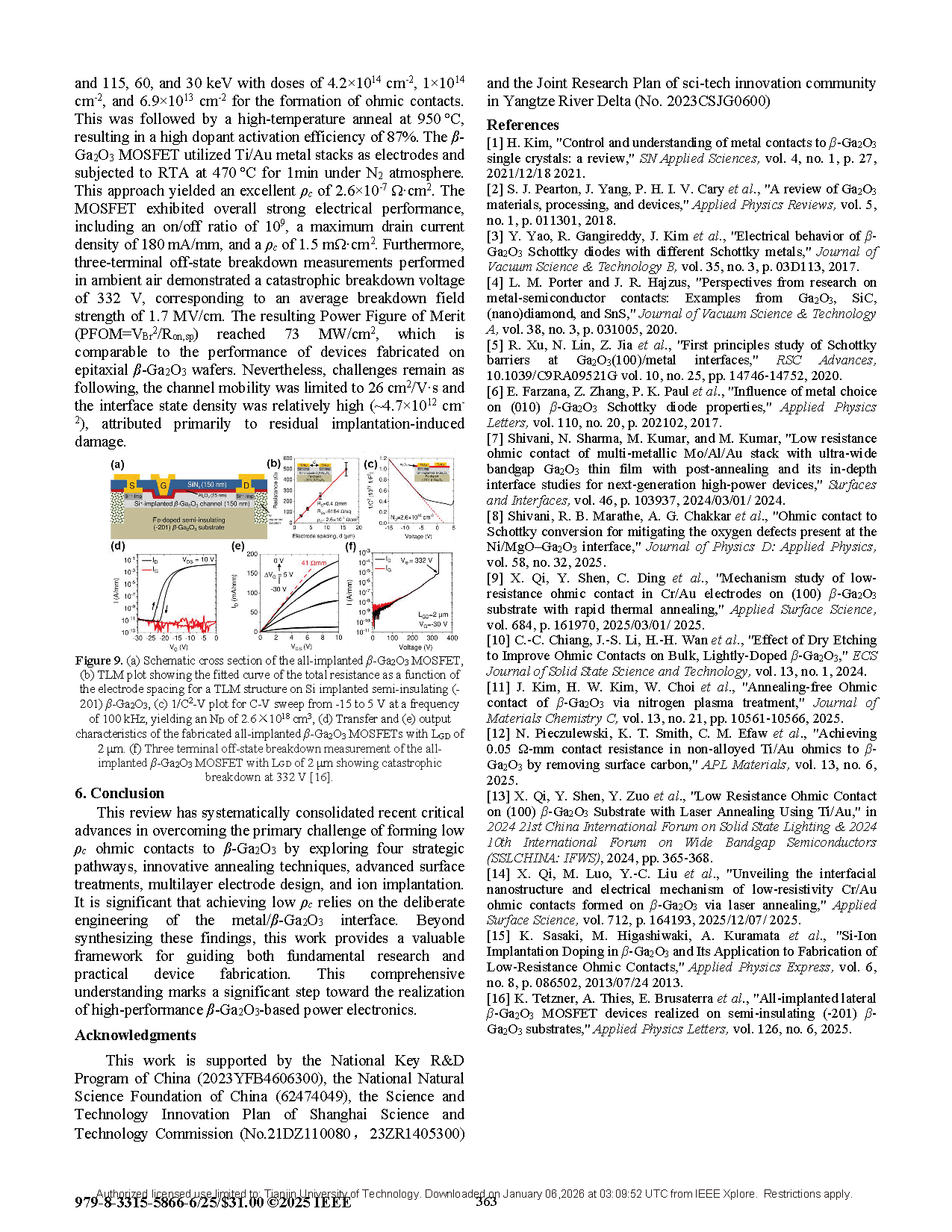
Figure 4. (a) Calculated temperature-dependent ρc using circular TLM on the etched surface with an etching condition of RF400 W/ICP 600W, (b)ρc with different etching conditions and annealing temperatures. The reference sample was an unetched control.
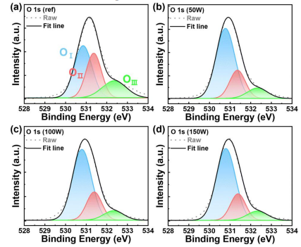
Figure 5. XPS spectra of O 1s peak of plasma treated β-Ga2O3 substrates with bias powers of (a) pristine, (b)50 W, (c) 100 W, and (d) 150 W[11].
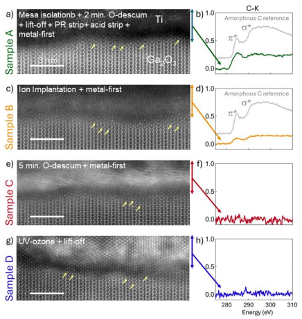
Figure 6. (a), (c), (e), and (g) Atomic resolution ADF-STEM images of the Ti/Ga2O3 interface along the [001] zone axis, (b), (d), (f), and (h) Normalized C–K EELS spectra acquired from the region across the Ti and Ga2O3 layers between the double-headed arrows of in (a), (c), (e), and (g), respectively [12].
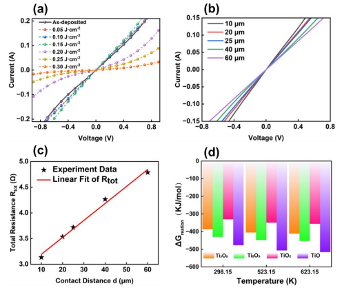
Figure 7. (a) I-V characteristics of TLM structures for Ti/Au contacts on β−Ga2O3 samples as a function of annealing temperature from 0.05 J·cm-2 to 0.3 J·cm-2, (b) Effect of spacing on I-V characteristics of Ti/Au electrodes Ti/Ga2O3 interface chemical reaction [13].
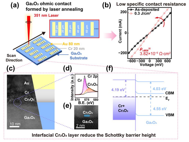
Figure 8. (a) Schematic of sample preparation, laser annealing, and LTLM patterning, (b) Electrical characteristics of LTLM structures incorporating Cr/Au contacts on β−Ga2O3, (c) TEM image of β−Ga2O3/Cr/Au, (d) Fine spectrum fitting of Cr 2p at the interface after annealing at 0.3 J/cm2 , (e) Cross-sectional high-resolution spherical aberration corrected TEM images, (f) Schematic representation of the band alignment at the Cr/Ga2O3 interface after laser annealing at 0.3 J/cm2 [14].
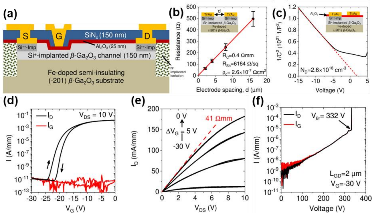
Figure 9. (a) Schematic cross section of the all-implanted β-Ga2O3 MOSFET, (b) TLM plot showing the fitted curve of the total resistance as a function of the electrode spacing for a TLM structure on Si implanted semi-insulating (-201) β-Ga2O3, (c) 1/C2-V plot for C-V sweep from -15 to 5 V at a frequency of 100 kHz, yielding an ND of 2.6×1018 cm3, (d) Transfer and (e) output characteristics of the fabricated all-implanted β-Ga2O3 MOSFETs with LGD of 2 μm. (f) Three terminal off-state breakdown measurement of the all-implanted β-Ga2O3 MOSFET with LGD of 2 μm showing catastrophic breakdown at 332 V [16].
DOI:
doi.org/10.1109/SSLCHINAIFWS69008.2025.11314970