Paper Sharing
【Member Papers】3-D Modeling for Electrical Optimization of Delta-Doped β-Ga₂O₃ MOSFETs With Anisotropic Electrothermal Properties
日期:2026-01-09阅读:444
Researchers from the Harbin Institute of Technology, Shenzhen have published a dissertation titled “3-D Modeling for Electrical Optimization of Delta-Doped β-Ga2O3 MOSFETs With Anisotropic Electrothermal Properties” in IEEE Transactions on Electron Devices. Dr. Yinfei Xie is the first author, and Prof. Huarui Sun is the corresponding author. This work presents a three-dimensional (3D) electrothermal coupling model to systematically investigate performance optimization pathways in β-Ga2O3 MOSFETs under electrothermal co-design frameworks, providing theoretical foundations and technical guidance for the design and fabrication of next-generation high-power gallium oxide devices.
Background
β-Ga2O3, an ultra-wide bandgap (UWBG) semiconductor, demonstrates exceptional potential for power electronics due to its high critical electric field (~8 MV/cm) and superior Baliga’s figure of merit (BFOM). However, its relatively low thermal conductivity significantly compromises device reliability and performance under high-power operation. Prior studies have predominantly focused on isolated electrical or thermal optimizations, lacking a systematic methodology for electro-thermal & structural co-design. Critically, the synergistic impacts of anisotropic mobility, thermal conductivity, channel orientation, and δ-doping process remain inadequately elucidated in existing literature.
Main content
Xie et al. developed a three-dimensional finite-element electrothermal coupling model using Silvaco TCAD to systematically analyze the impacts of temperature- and orientation-dependent electron mobility, thermal conductivity, channel orientation, and δ-doping on the electrical performance of β-Ga2O3 MOSFETs. Results show that thermal conductivity anisotropy exerts a more pronounced influence than mobility anisotropy, emerging as the dominant factor in device performance. A 45° (010)-oriented channe, exhibiting the highest in-plane thermal conductivity, demonstrates optimal electrical performance and heat dissipation. Optimal δ-doping charge density exists at 5×1013 cm⁻2, which broadens the depletion region and enhances breakdown voltage (Vbr), yet excessive doping induces localized breakdown risks. Proximity of δ-doping layers to the channel interface improves electric field uniformity and Vbr but introduces scattering centers when overly close, degrading reliability. Through synergistic optimization of channel orientation, δ-doping position, and charge density, the team achieved a β-Ga2O3 MOSFET with Vbr = 2284 V, power figure of merit (PFOM) = 369.5 MV/cm2, and specific on-resistance (RON,sp) = 14.1 mΩ·cm2, approaching the theoretical limits of β-Ga2O3 material.
Highlight
1、Modeling Innovation: A three-dimensional (3D) anisotropic electro-thermal & structural coupled simulation platform was established, enabling multiphysics co-design and performance prediction for β-Ga2O3 MOSFETs.
2、Mechanistic Insight: The dominant role of thermal conductivity anisotropy in determining electrical performance was clarified, leading to the proposal of a electro-thermal & structural optimization strategy.
3、Design Guidance: Through synergistic control of δ-doping and channel orientation, simultaneous optimization of breakdown voltage (Vbr) and specific on-resistance (RON,sp) was achieved, offering a feasible road-map for high-performance power MOSFET design.
Conclusion
This study systematically demonstrates the feasibility and methodological framework of performance optimization in β-Ga2O3 MOSFETs through electro-thermal & structural co-design. The findings reveal that strategic utilization of material anisotropy, combined with optimized channel orientation and δ-doping processes, substantially enhances device reliability and efficiency under high-power operating conditions. This work not only advances the theoretical development of gallium oxide power devices but also establishes a paradigm for multiphysics co-design in wide-bandgap semiconductor devices.
Project Support
This work was supported in part by the Guangdong Special Support Program (2021TQ06C953), the Shenzhen Science and Technology Program (JCYJ20190806142614541), and the Open Research Fund of State Key Laboratory of Materials for Integrated Circuits (SKLIC-K2024-04).
Team Introduction

Huarui Sun is a Professor, Doctoral Supervisor, and Associate Dean of the School of Science at Harbin Institute of Technology, Shenzhen. His research focuses on characterization of semiconductor materials and devices, with recent work advancing thermal analysis methods for wide-bandgap semiconductors, revealing the origins of thermal resistance, and establishing electro-thermal co-design strategies. He also clarified the physical origin and modulation mechanisms of Raman anisotropy in two-dimensional semiconductors.
He has published over 70 papers in high-impact journals such as Physical Review Letters, Laser & Photonics Reviews, and Nature-family journals, holds more than ten invention patents, and was awarded the Guangdong Provincial Young Top-notch Talent in Science and Technology Innovation. He serves as a Young Editorial Board Member of Journal of Synthetic Crystals and an Executive Committee Member of the Surface Analysis Division of the Guangdong Association of Analytical Testing.

Yinfei Xie is a Ph.D. candidate in Physics at Harbin Institute of Technology, Shenzhen, specializing in thermal reliability and electro-thermal co-optimization of ultra-wide bandgap semiconductor devices. He published over 10 SCI papers in prestigious international journals and conferences, including Cell Reports Physical Science, Nano Letters, Nano Research, ACS Applied Materials & Interfaces, Applied Physics Letters, IEEE Transactions on Electron Devices, and IEEE EDTM.
Dr. Xie holds ten Chinese national patents (filed or granted). He has received several honors and awards, such as the inaugural China Association for Science and Technology (CAST) Young Talent Support (Doctoral Candidate), National Scholarship for Doctoral Students, Outstanding Scientific and Technological Talent of Heilongjiang Provincial Association for Science and Technology, and Outstanding Graduate Student of Heilongjiang Province.
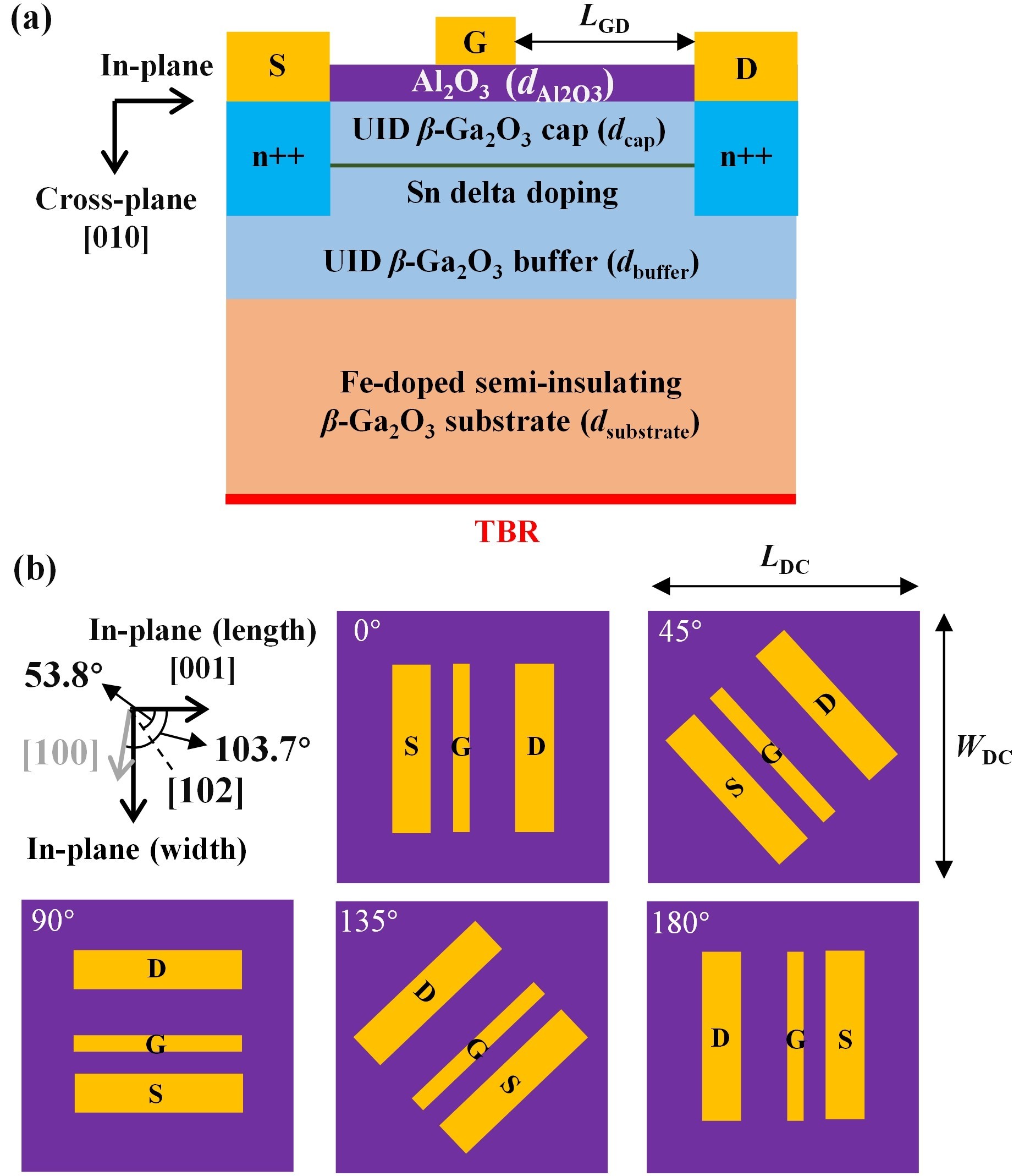
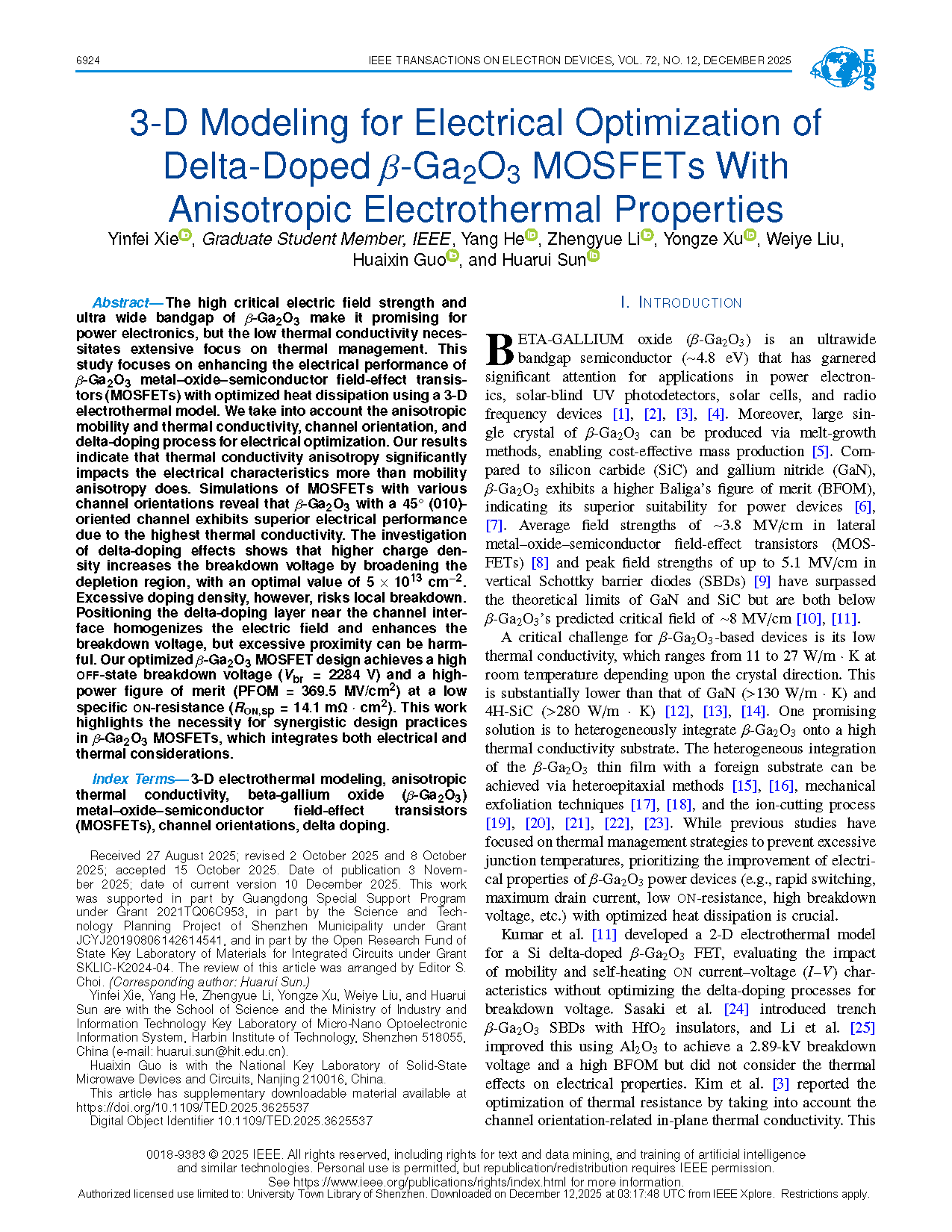
Fig. 1. Cross-sectional schematic of the β-Ga2O3 MOSFET (not drawn to scale). An effective TBR is added at the bottom of the substrate layer. (b) Top-view schematic diagrams of five representative channel directions rotated 0°, 45°, 90°, 135°, and 180° within the plane.
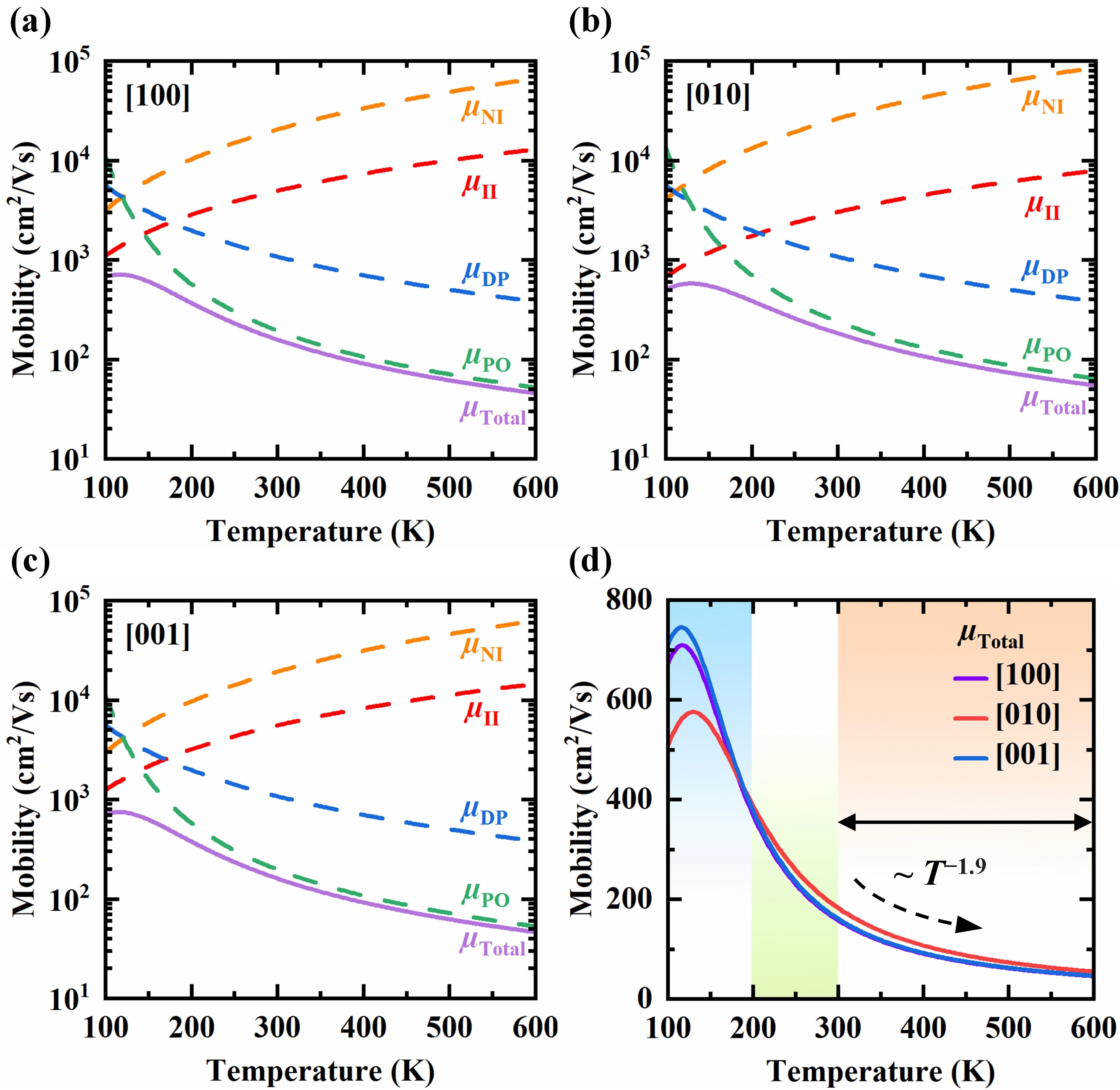
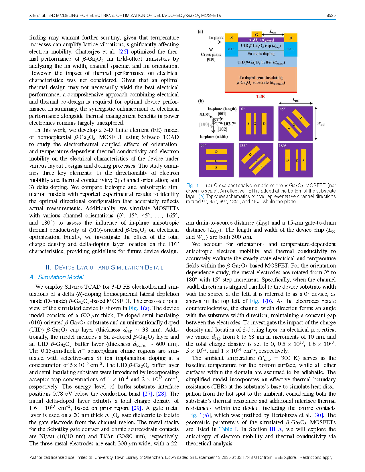
Fig. 2. Calculated temperature-dependent electron mobilities along the crystal orientations of (a) [100], (b) [010], (c) [001], and (d) a comparison of three total mobilities μTotal, respectively.
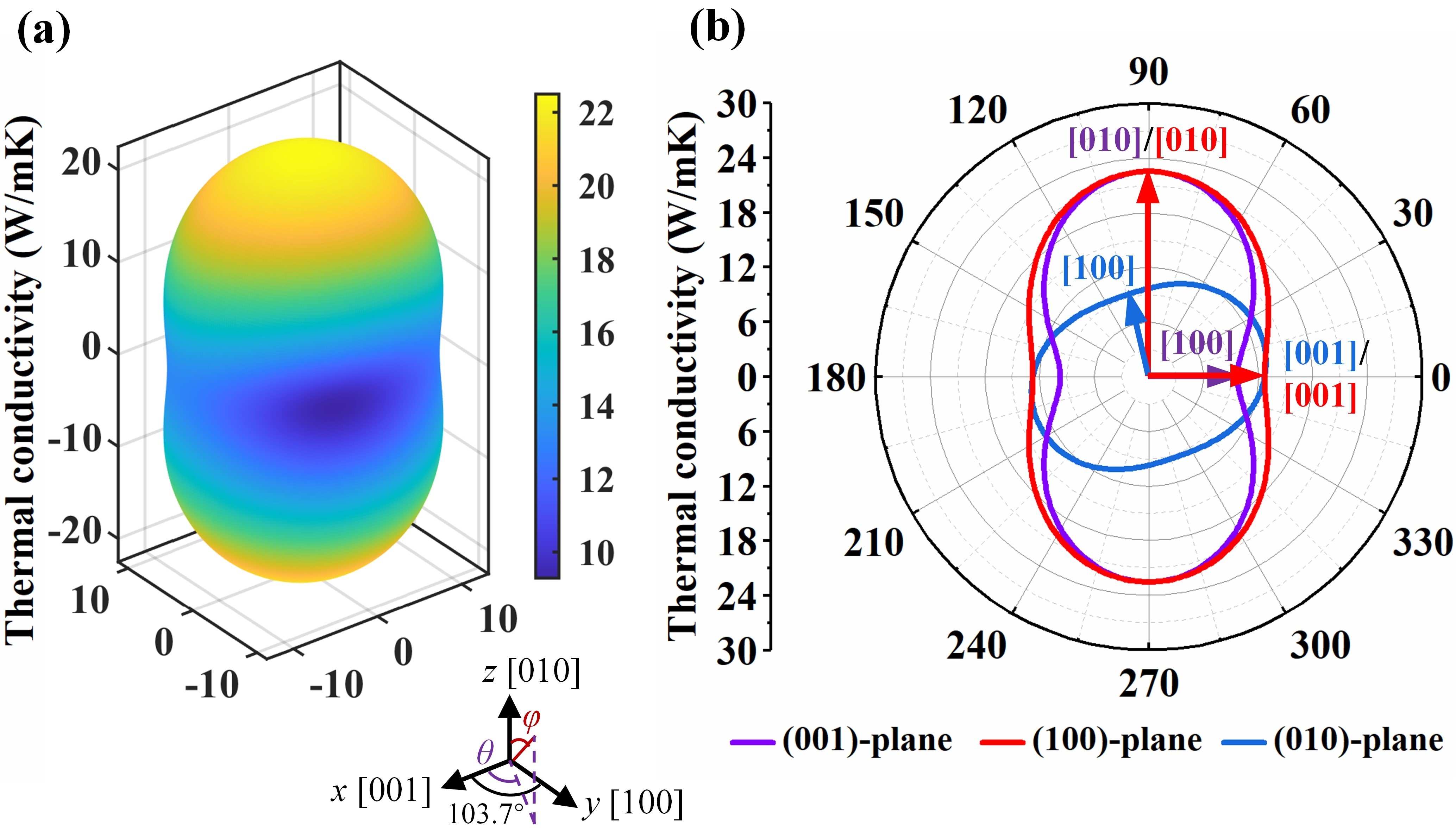
Fig. 3. (a) Calculated 3D directional thermal conductivity of β-Ga2O3 at room temperature. (b) Projection of 3D thermal conductivity tensor of β-Ga2O3 on (001)-, (100)-, and (010)-plane.
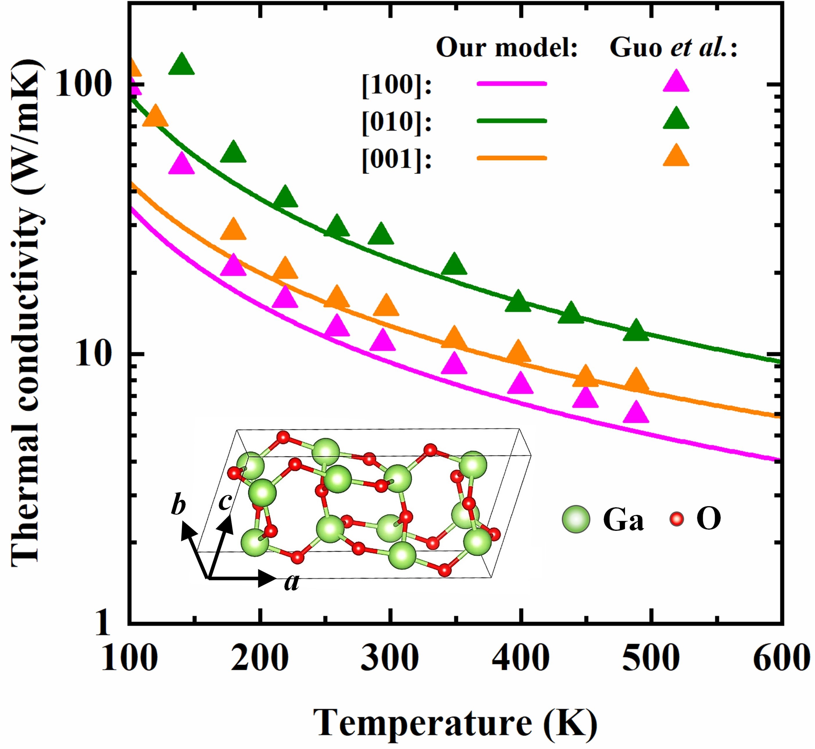
Fig. 4. Calculated temperature-dependent thermal conductivities along crystal orientations of [100], [010], and [001].
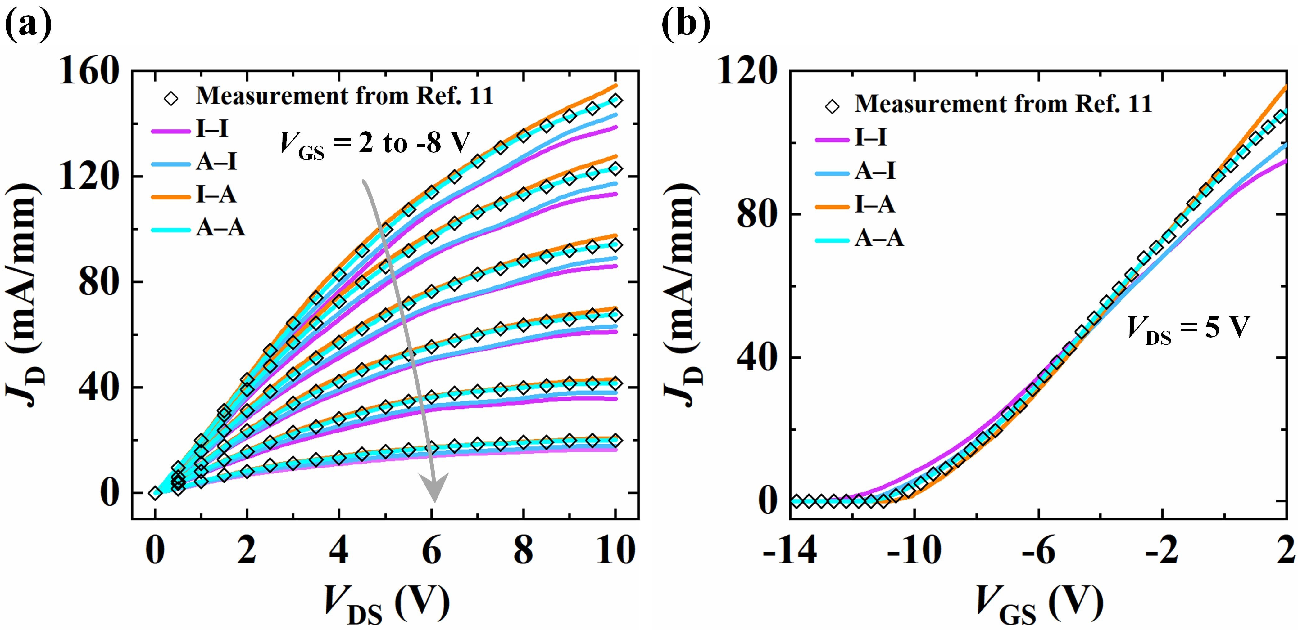
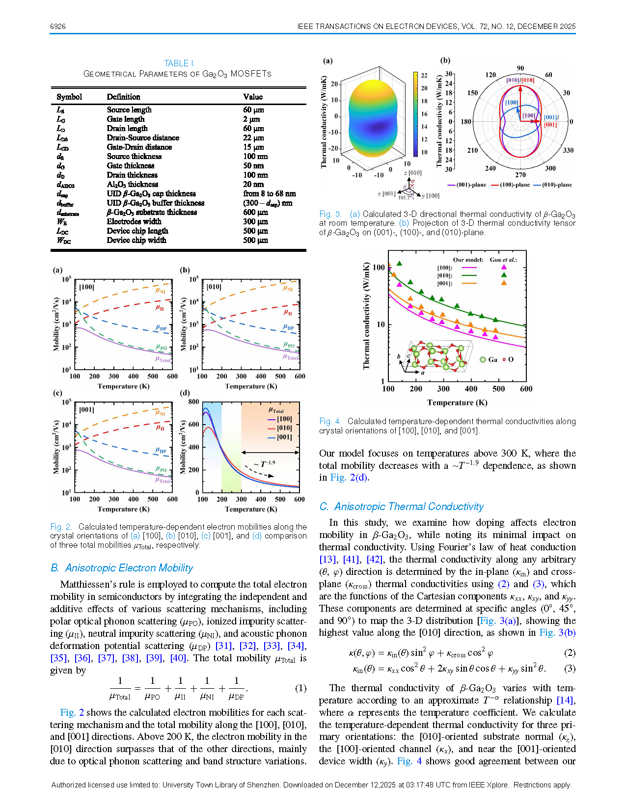
Fig. 5. Comparison between the experimentally measured [11] and our electrothermal simulated (a) output and (b) transfer characteristics for various configurations: isotropic–isotropic (I–I), anisotropic–isotropic (A–I), isotropic–anisotropic (I–A), and anisotropic–anisotropic (A–A).
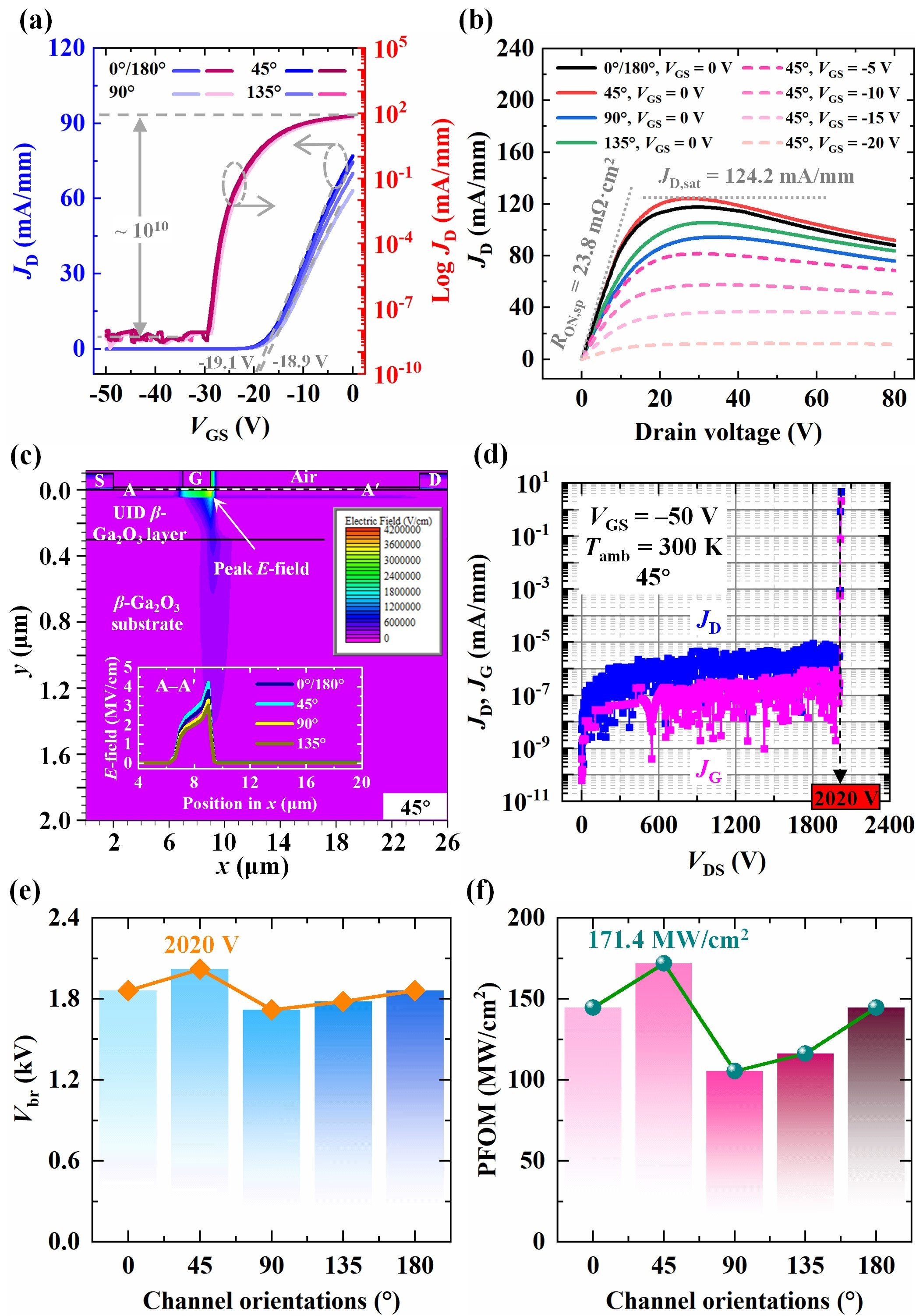
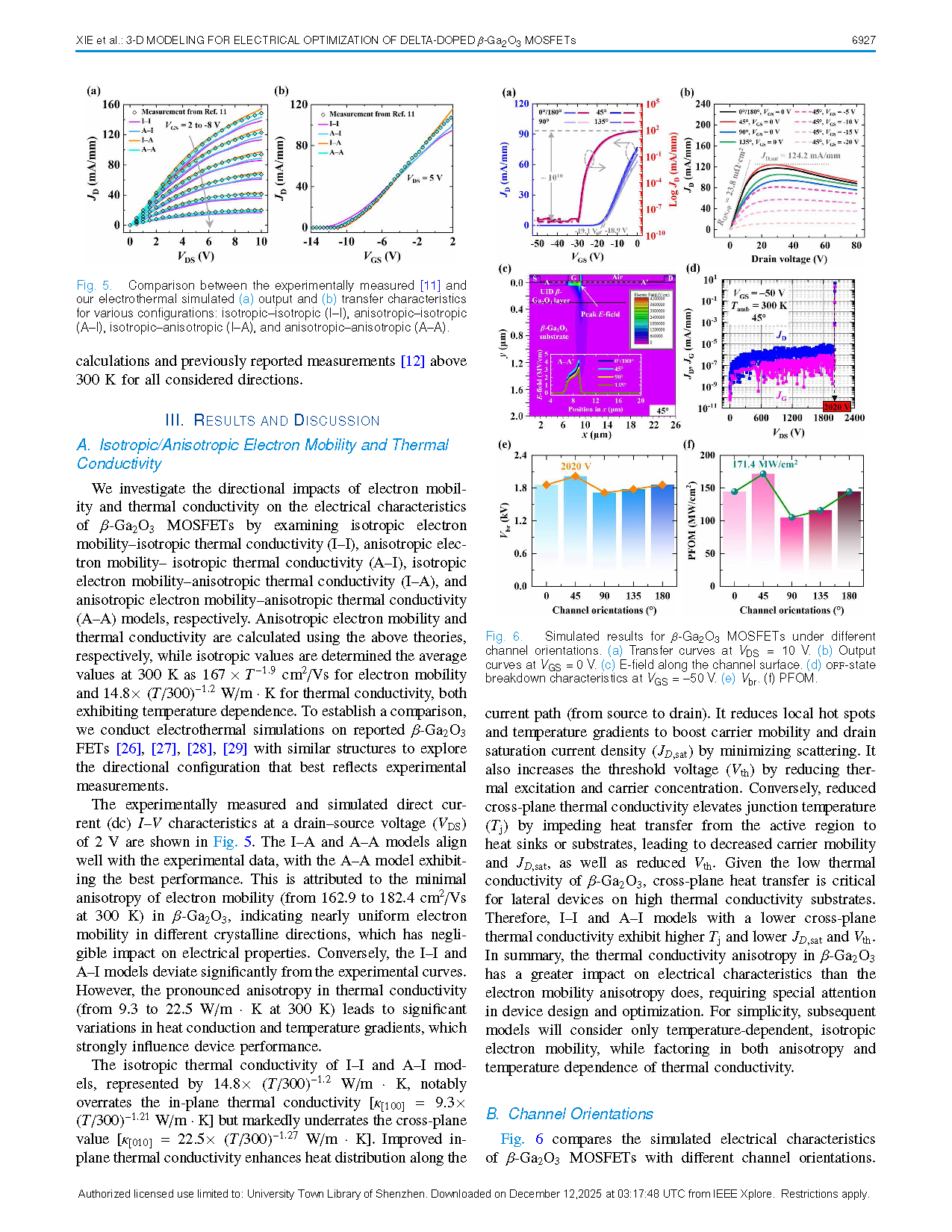
Fig. 6. Simulated results for β-Ga2O3 MOSFETs under different channel orientations: (a) transfer curves at VDS = 10 V, (b) output curves at VGS = 0 V, (c) E-field along the channel surface, (d) off-state breakdown characteristics at VGS = −50 V, (e) Vbr, and (f) PFOM.
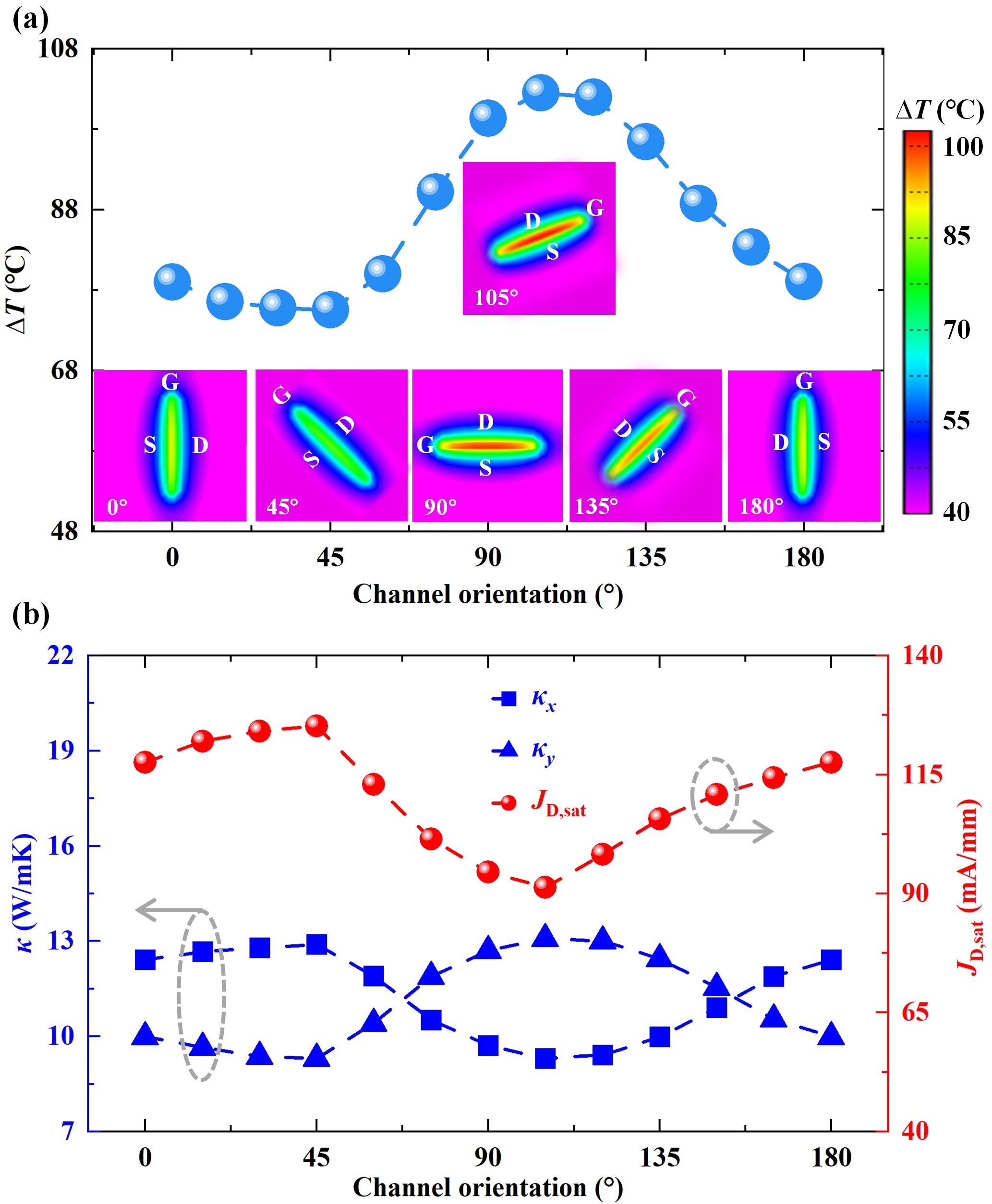
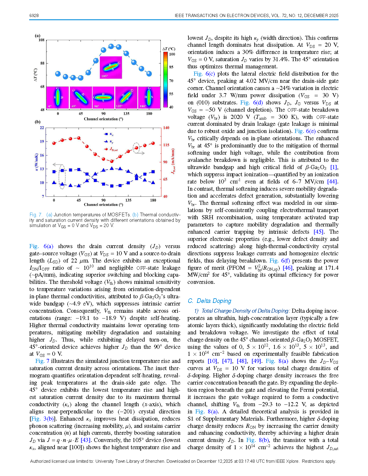
Fig. 7. (a) Junction temperatures of MOSFETs, and (b) thermal conductivity and saturation current density with different orientations obtained by simulation at VGS = 0 V and VDS = 20 V.
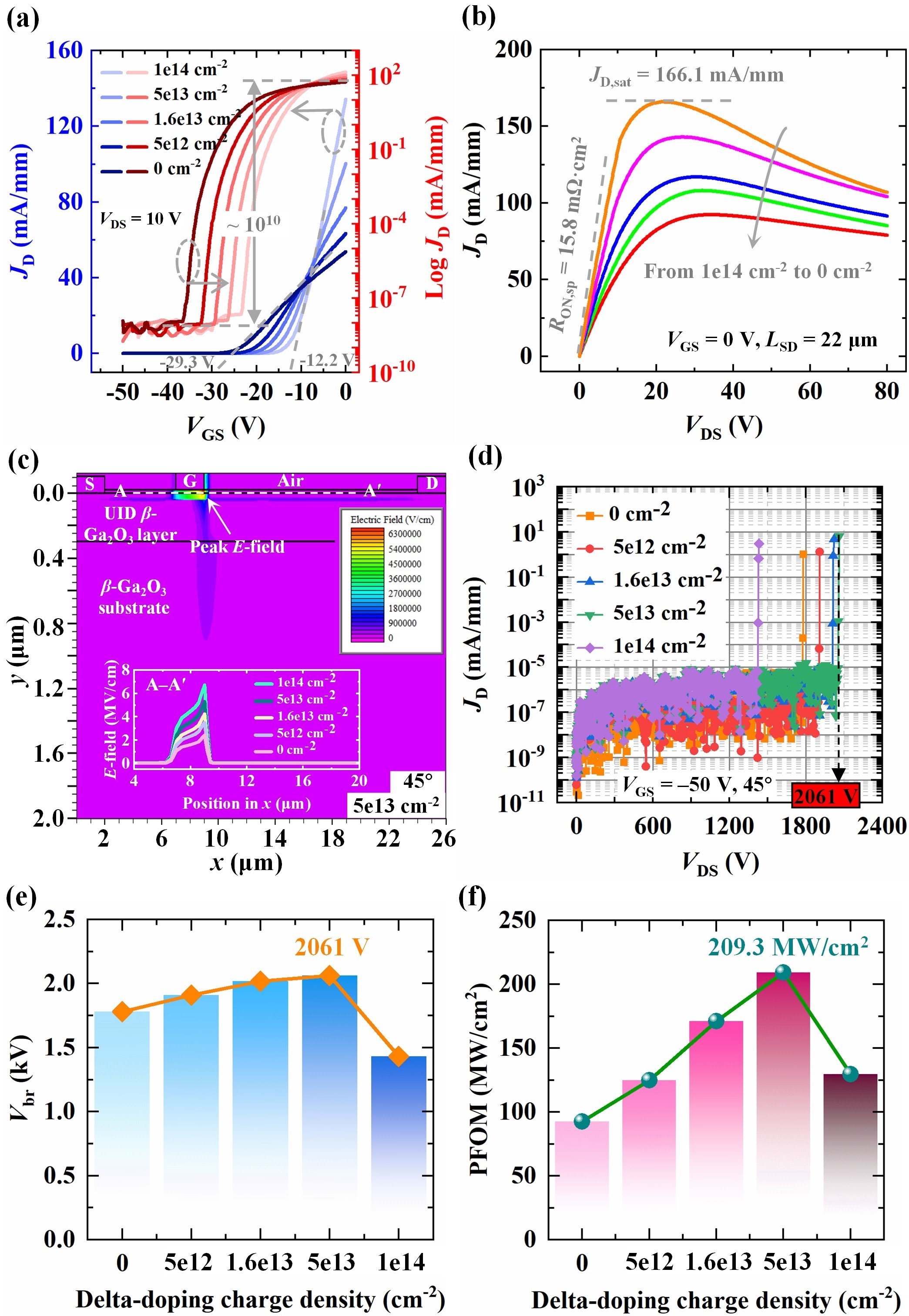
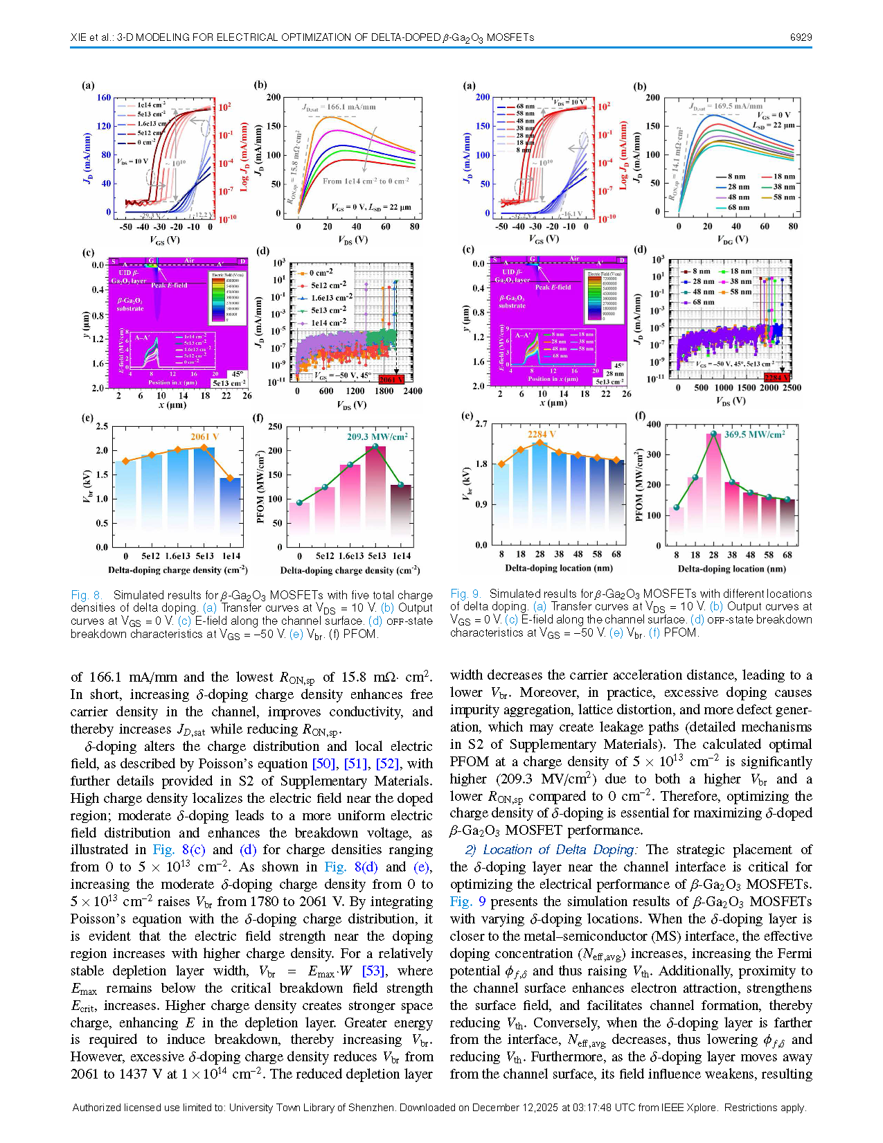
Fig. 8. Simulated results for β-Ga2O3 MOSFETs with five total charge densities of delta-doping: (a) transfer curves at VDS = 10 V, (b) output curves at VGS = 0 V, (c) E-field along the channel surface, (d) off-state breakdown characteristics at VGS = −50 V, (e) Vbr, and (f) PFOM.
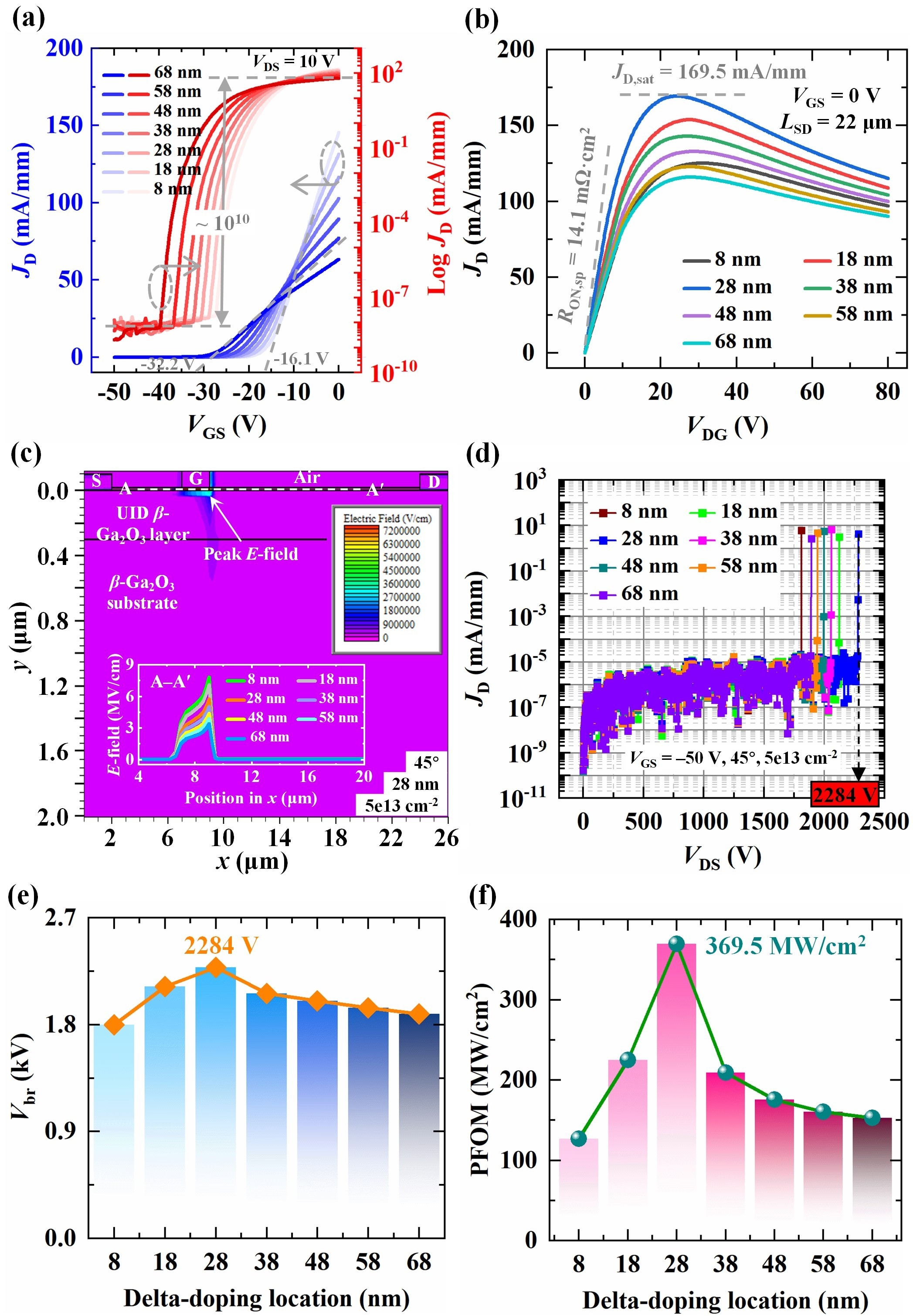
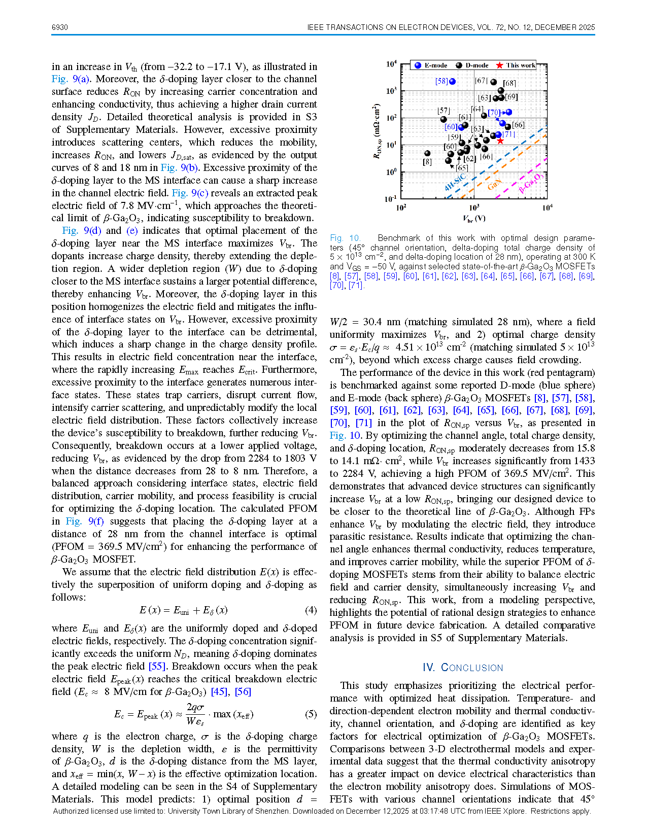
Fig. 9. Simulated results for β-Ga2O3 MOSFETs with different locations of delta-doping: (a) transfer curves at VDS = 10 V, (b) output curves at VGS = 0 V, (c) E-field along the channel surface, (d) off-state breakdown characteristics at VGS = −50 V, (e) Vbr, and (f) PFOM.
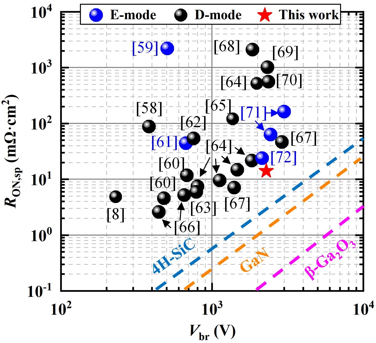
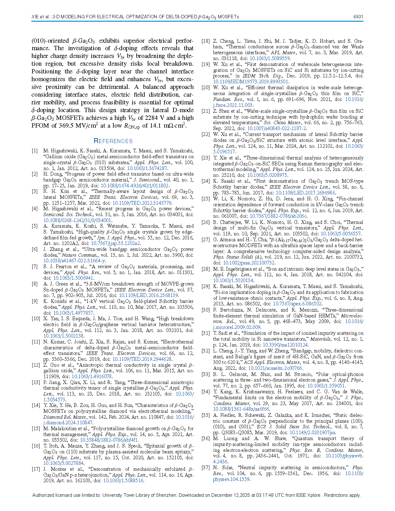
Fig. 10. Benchmark of this work with optimal design parameters (45° channel orientation, delta-doping total charge density of 5 × 1013 cm−2, and delta-doping location of 28 nm), operating at 300 K and VGS = −50 V, against selected state-of-the-art β-Ga2O3 MOSFETs [8], [58]-[72].
Paper Information:
Title: 3-D Modeling for Electrical Optimization of Delta-Doped β-Ga2O3 MOSFETs With Anisotropic Electrothermal Properties
Authors: Yinfei Xie, Yang He, Zhengyue Li, Yongze Xu, Weiye Liu, Huaxin Guo, Huarui Sun
Journal: IEEE Transactions on Electron Devices
DOI: 10.1109/TED.2025.3625537