Paper Sharing
【Domestic Papers】Quasi-2D gallium oxide X-ray detector
日期:2026-01-12阅读:404
Researchers from the State Key Laboratory of Cryogenic Science and Technology, Technical Institute of Physics and Chemistry, Chinese Academy of Sciences have published a dissertation titled "Quasi-2D gallium oxide X-ray detector" in Communications Materials.
Project Support
This work was partially supported by the NSFC Grant (No. 91748206).
Background
X-rays are electromagnetic waves with extremely short wavelengths and strong penetrating ability, which have been widely used in the fields of industrial nondestructive testing, medical imaging and radiation therapy, security systems and aerospace. The growing demand for X-ray detectors is putting forward higher performance requirements from the early days of film, calorimetry and other traditional detection methods, to the gradually developed pyroelectricity, glow exhaustion fluorescence, scintillator and other indirect detection technology and direct detection technology such as ionization chambers. The commonly used X-ray detectors can be roughly divided into three categories according to their different working mechanisms: gas detectors, scintillator detectors and semiconductor detectors.
Abstract
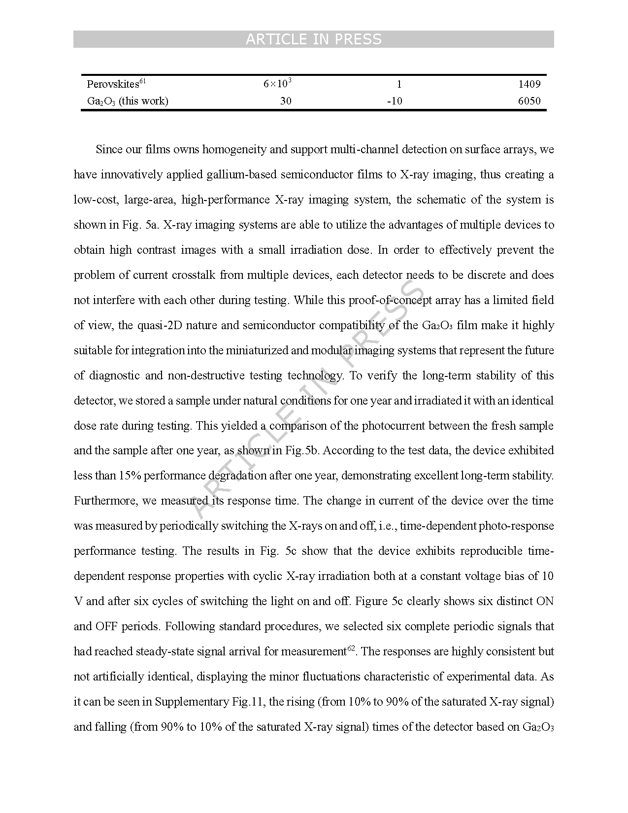
X-rays, characterized by their short wavelength and high penetrating power, are indispensable across numerous fields. Current X-ray detection relies heavily on amorphous selenium (a-Se) and medium bandgap semiconductors (e.g., Si, CdTe, CZT), which often face limitations including complex large-scale fabrication, high cost, and stability issues under intense irradiation. While alternative wide-bandgap materials like diamond offer excellent performance, challenges related to scalable fabrication and cost often remain. Here, we report a high-performance X-ray detector based on solution-processed quasi-two-dimensional (2D) gallium oxide (Ga₂O₃) films fabricated via a novel liquid metal nano-printing technique. Leveraging the ultra-wide bandgap and high quality of the printed Ga₂O₃, the device achieves an ultra-high sensitivity of 6050 μC/Gy/cm². We further demonstrate the practical utility of these detectors by integrating them into a functional X-ray imaging system. This work establishes liquid metal nano-printing as a vital pathway for the rapid fabrication of ultrathin, high-performance, low-power-consumption X-ray detectors. Additionally, this work enables low-dose, high-resolution X-ray imaging for medical diagnostics and non-destructive testing, demonstrating a cost-effective pathway toward portable radiation detection systems.
Conclusion
In summary, we demonstrate a novel low-cost printing process for quasi-2D Ga2O3 and X-ray detectors. This straightforward and efficient method enables rapid large-area fabrication of quasi2D Ga2O3 with uniform film quality and thickness control, providing a critical foundation for achieving high spatial resolution in pixelated arrays. Simultaneously, the wide bandgap (~ 4.26 eV) and low dark current of quasi-2D Ga2O3 inherently favor potential-resolution detection by suppressing noise sources that degrade energy resolution in narrow-gap materials. Meanwhile, the wide bandgap (∼4 eV) and low dark current of quasi-2D Ga₂O₃ create inherent advantages for potential energy-resolved detection by suppressing noise sources that degrade energy discrimination in narrow-gap materials. We systematically study the detection performance of the detector, showing good spatial resolution and energy resolution, large differences in the responsivity to different intensities of X-rays (slope), and the logarithm responsivity and the X-ray intensity with a good linear relationship (R-squared), in terms of spatial resolution, the tiny detector element (element linearity) to ensure that the device can be in the mm precision detection of the intensity distribution of spatial X-rays. The device exhibits a falling-edge response time of less than 45 ms, which proves that the device has a good transient response to X-rays, and this also lays a solid foundation for new CT imaging. We have also constructed an 8×8 X-ray detection imaging array system based on amorphous quasi-2D Ga2O3 using liquid metal nanoimprinting technology for the first time. This work provides a simple, efficient and low-cost new strategy for large-area, high-quality and controllable preparation of next-generation high-performance X-ray detectors and imaging systems, which is of great significance and value for the development of sensitive, fast and stable X-ray imaging detectors and even CT core detection components. While this study focuses on foundational sensitivity and low-voltage operation metrics, quantitative spatial/energy resolution measurements require pixelated array integration and spectroscopic characterization – important next steps for practical implementation.
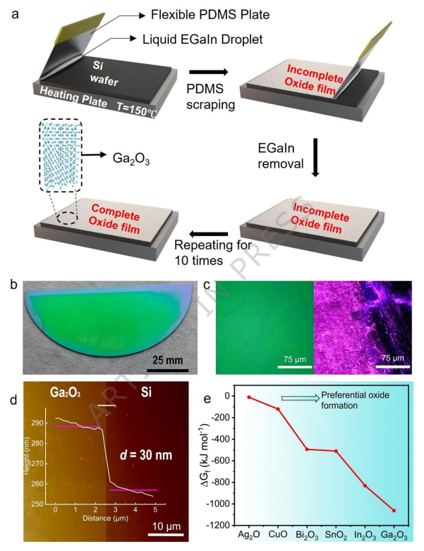
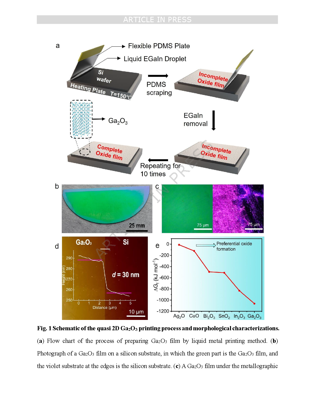
Fig. 1 Schematic of the quasi 2D Ga2O3 printing process and morphological characterizations. (a) Flow chart of the process of preparing Ga2O3 film by liquid metal printing method. (b) Photograph of a Ga2O3 film on a silicon substrate, in which the green part is the Ga2O3 film, and the violet substrate at the edges is the silicon substrate. (c) A Ga2O3 film under the metallographic microscope. The left image is the bright field, observing its surface uniformity and flatness, and the right image is the dark field, observing whether there are noise and defects on its surface. (d) AFM image at the step of the Ga2O3 film, showing its thickness of about 30 nm. (e) Schematic of standard formation Gibbs free energy change for common metals in liquid metal systems. The line between the formation energies indicates a guideline to the eye.
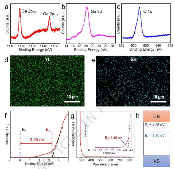
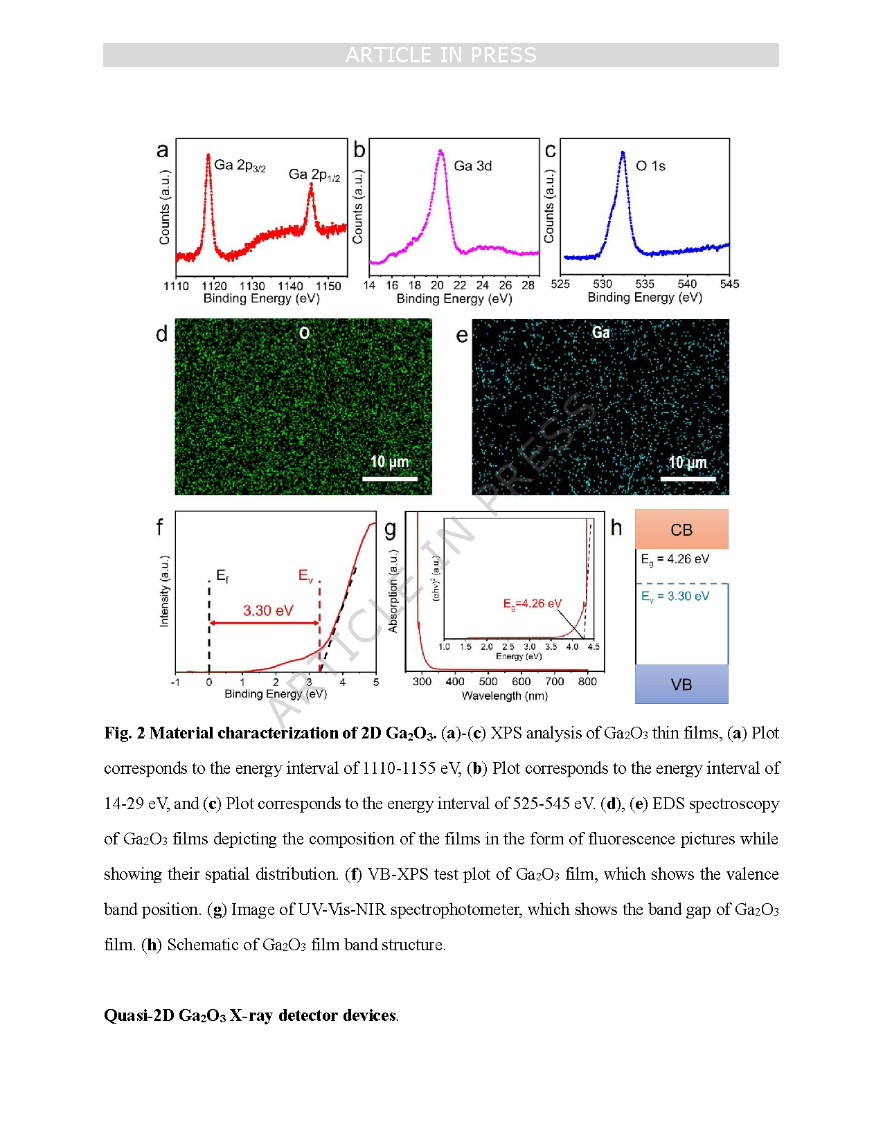
Fig. 2 Material characterization of 2D Ga2O3. (a)-(c) XPS analysis of Ga2O3 thin films, (a) Plot corresponds to the energy interval of 1110-1155 eV, (b) Plot corresponds to the energy interval of 14-29 eV, and (c) Plot corresponds to the energy interval of 525-545 eV. (d), (e) EDS spectroscopy of Ga2O3 films depicting the composition of the films in the form of fluorescence pictures while showing their spatial distribution. (f) VB-XPS test plot of Ga2O3 film, which shows the valence band position. (g) Image of UV-Vis-NIR spectrophotometer, which shows the band gap of Ga2O3 film. (h) Schematic of Ga2O3 film band structure.
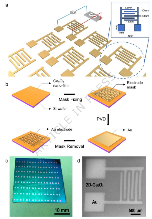
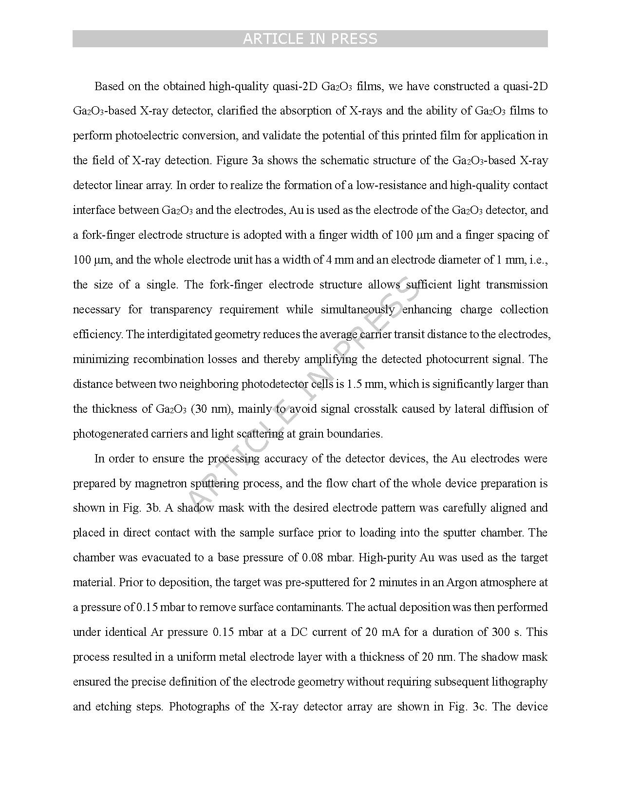
Fig. 3 Printing of Ga2O3-based X-ray detector arrays. (a) Design diagram of the interdigitated electrode, the upper figure shows the detailed parameters of a single interdigitated electrode, and the lower figure shows the layout of the interdigitated electrode array, with the array size of 8×8. (b) Flow chart of electrode evaporation, firstly, the mask is fixed on the prepared Ga2O3 thin film, and then after fixing it completely, PVD evaporation is carried out, and then after the evaporation is completed, the mask is removed and the electrode array is obtained. (c) Photographs of electrode array, it can be seen that the evaporation electrode layout is very even and clear. (d) Individual electrodes under SEM, under this scale, the electrodes still maintain a very clear contour as well as a homogeneous surface, and the inserted teeth are not distorted and fuzzy, and other defects appear.
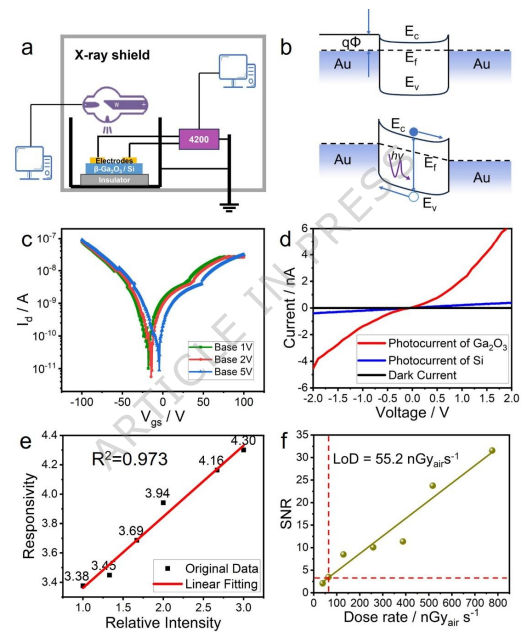
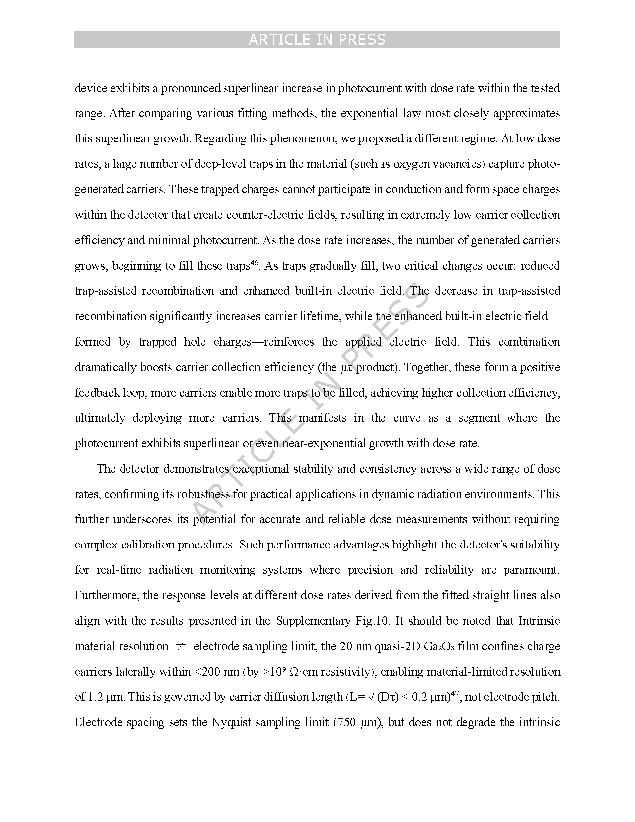
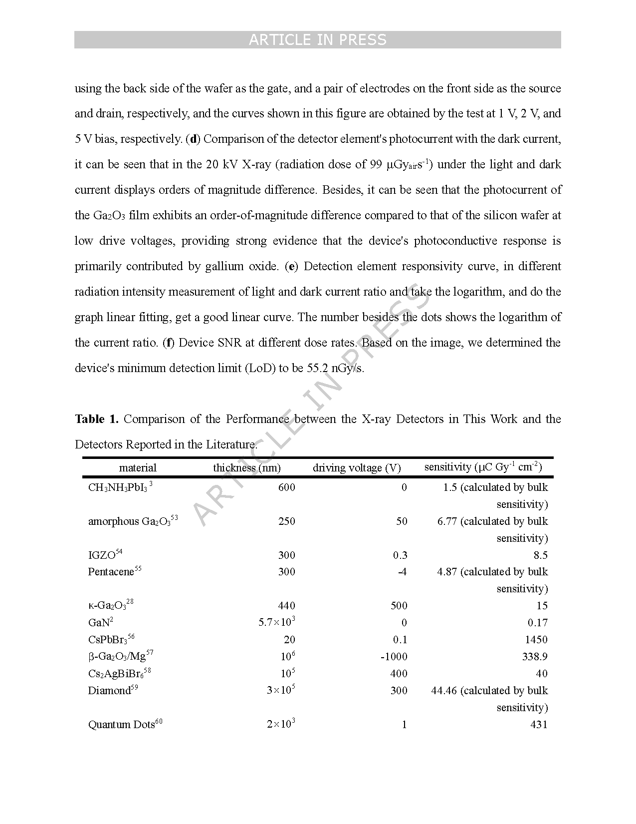
Fig. 4 Optoelectronic properties of printed Ga2O3-based X-ray detector. (a) Schematic diagram for detection system. The Keithley 4200 Source Meter Unit was connected in series to apply bias and simultaneously measure the current generated by the Ga2O3 detector. (b) Schematic diagram of electron transition by X-ray motivation. (c) Tri-pole I-V curve of the detector element, using the back side of the wafer as the gate, and a pair of electrodes on the front side as the source and drain, respectively, and the curves shown in this figure are obtained by the test at 1 V, 2 V, and 5 V bias, respectively. (d) Comparison of the detector element's photocurrent with the dark current, it can be seen that in the 20 kV X-ray (radiation dose of 99 μGyairs-1) under the light and dark current displays orders of magnitude difference. Besides, it can be seen that the photocurrent of the Ga2O3 film exhibits an order-of-magnitude difference compared to that of the silicon wafer at low drive voltages, providing strong evidence that the device's photoconductive response is primarily contributed by gallium oxide. (e) Detection element responsivity curve, in different radiation intensity measurement of light and dark current ratio and take the logarithm, and do the graph linear fitting, get a good linear curve. The number besides the dots shows the logarithm of the current ratio. (f) Device SNR at different dose rates. Based on the image, we determined the device's minimum detection limit (LoD) to be 55.2 nGy/s.
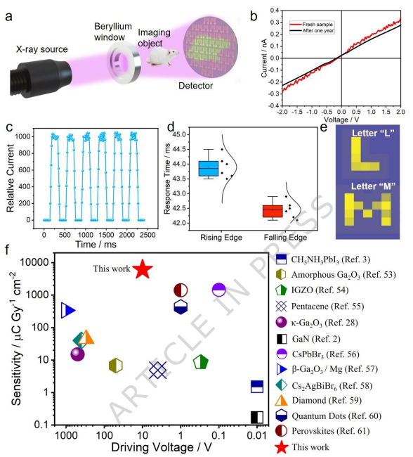
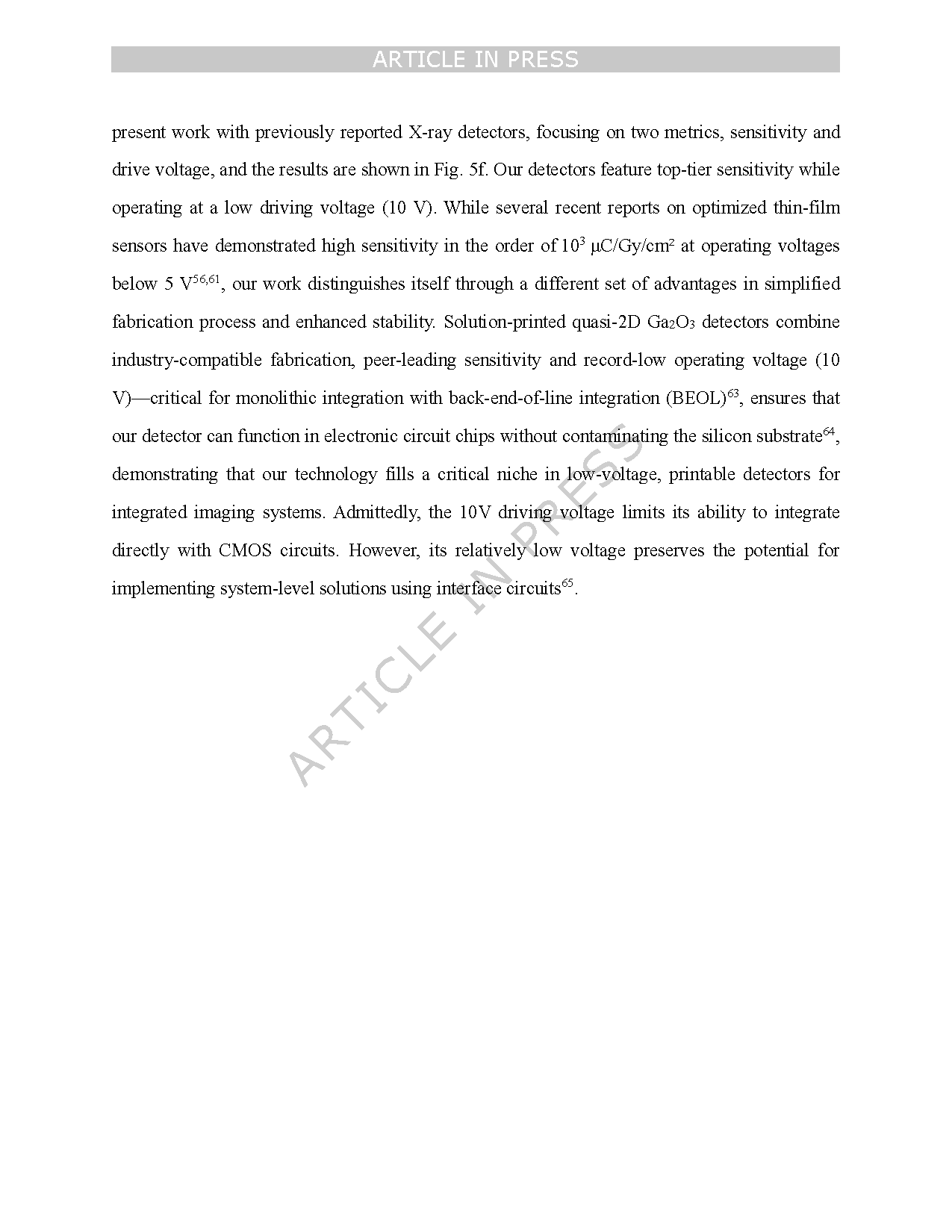
Fig. 5 X-ray imaging output of Ga2O3 detectors. (a) Schematic diagram of X-ray imaging. The field of view in this direct-irradiation configuration is constrained by the physical area of the 8×8 array (approximately 3.2 × 3.2 cm2), limiting the object size for a single-shot image. Future systems could incorporate optical focusing elements or scanning mechanisms to image larger objects. The animal on the schematic represents any object. (b) Comparison of photocurrent between fresh samples and the same samples after one year. Samples stored under ambient conditions for one year exhibited photocurrent responses close to those of fresh samples, demonstrating the device's excellent long-term stability. (c) Response time test of the detector, were measured six cycles, with the average response time of the rising edge as 43.8 ms, while the falling edge response time as 42.5 ms, at the same time. The relative current of the illumination is around 1000, which shows that it owns the characteristics of cyclic stability. (d) Box plots of the rising and falling edge response times of the detector, with the boxes indicating the Q1 through Q3 bins, the error bar reflecting the extreme deviation of each set of data, and the normal curve showing the distribution of response times. (e) Imaging validation effect diagram of the detector, using 1mm thickness of copper shielding X-rays, and measure its relative current, high relative current is marked in blue, low relative current is marked in yellow. The imaging of the “L” and “M” letters are clearly seen. Further, the corner and the structure are clearly displayed. (f) Comparison of detector performance, our work is marked as a red pentagram in the figure.
DOI:
doi.org/10.1038/s43246-025-01053-1