Paper Sharing
【Domestic Papers】Designing a Hybrid α/β-Ga₂O₃ Polymorph Heterostructure from Strain-Relaxed Phase Transition for High-Voltage Power Diodes
日期:2026-01-12阅读:370
Researchers from the NIMTE Chinese Academy of Sciences and Yongjiang Laboratory, have published a research paper titled "Designing a Hybrid α/β-Ga2O3 Polymorph Heterostructure from Strain-Relaxed Phase Transition for High-Voltage Power Diodes" in Materials Today Physics.
Project Support
This research was supported by the National Natural Science Foundation of China (Grant No. 62304227), the China Postdoctoral Science Foundation (Grant No. 2025M773410), the Zhejiang Provincial Natural Science Foundation of China (Grant Nos. LQ23F040005 and LQN25F040011), and the Ningbo Yongjiang Talent Introduction Programme (Grant Nos. 2021A-046-C and 2024A-441-G).
Background
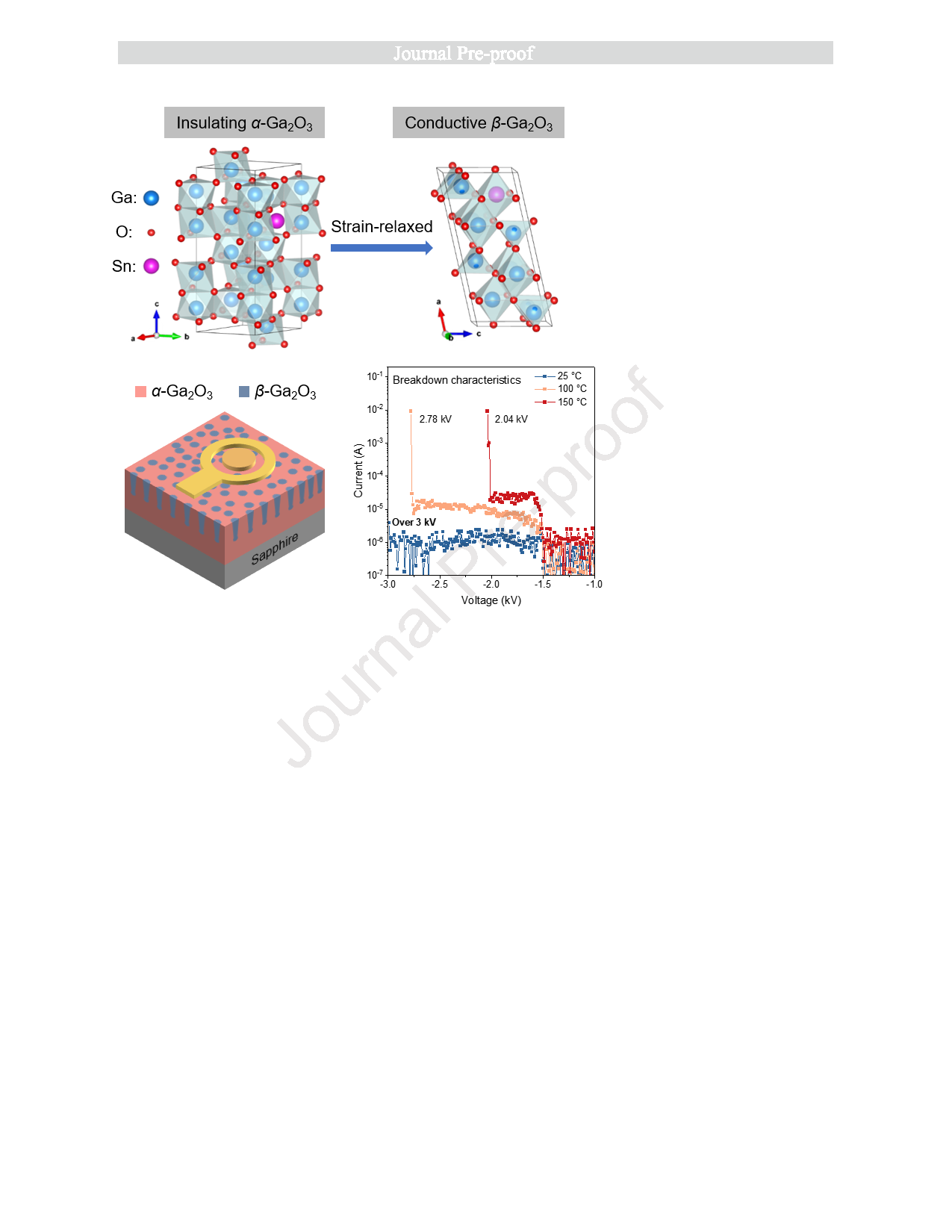
Gallium oxide (Ga2O3), as an emerging ultra-wide bandgap semiconductor, demonstrates great potential for high-power electronic applications. Its different crystal phases exhibit distinct properties: the corundum-structured α-Ga2O3 possesses the widest bandgap (~5.3 eV) and a high theoretical breakdown field, leading to a superior Baliga’s figure of merit; whereas the monoclinic β-Ga2O3 offers shallower donor levels and favorable carrier transport capabilities. In recent years, integrating different Ga2O3 polymorphs into heterostructures to harness the advantages of both phases has emerged as an attractive device design strategy. However, this requires careful control over phase formation, distribution, and dopant activation during heteroepitaxy. In previous studies, strain-driven α-to-β phase transition is considered detrimental to film quality and device performance. Here, we propose a strategy that utilizes this phase transition behavior to construct an α/β-Ga2O3 phase-mixed structure. The films based on this structure exhibit unique defect and transport characteristics, significantly enhancing the breakdown performance of lateral Schottky barrier diodes.
Abstract
Ultrawide bandgap (UWBG) gallium oxide (Ga2O3) featuring several polymorphs holds great potential for high-power electronics and solar-blind optoelectronics. Designing electronic devices based on hybrid Ga2O3 polymorph structures appears highly attractive, but it meets persistent obstacles from epitaxy challenges and dopant activation problems. This study reports a 3 kV-class lateral Schottky barrier diode (SBD) based on a unique heteroepitaxial α/β-Ga2O3 heterostructure composed of conductive β-Ga2O3 domains embedded in an insulating α-Ga2O3 matrix. The α/β-Ga2O3 heterostructure is constructed from a strain-relaxed α-to-β Ga2O3 phase transition that strongly depends on the substrate orientation and film thickness. The formation of the β-Ga2O3 phase presents a minor impact on the crystallinity of the α-Ga2O3 matrix and exhibits more readily dopant activation during the sputtering growth. The lateral SBD based on this hybrid α/β-Ga2O3 heterostructure combines the benefits of efficient carrier transport in β-Ga2O3 and the superior breakdown field in α-Ga2O3, thus enabling a decent rectifying behavior and a 3 kV breakdown voltage two times larger than the single-phase β-Ga2O3 diode. This study provides critical insights into the phase-design strategy for developing advanced UWBG electronic devices.
Highlights
● Low-dislocation-density α-Ga2O3 films are grown via magnetron sputtering.
● An α/β-Ga2O3 heterostructure is designed that exhibits unique defect characteristics.
● A 3 kV-class lateral SBD is demonstrated using the α/β-Ga2O3 heterostructure.
Conclusions
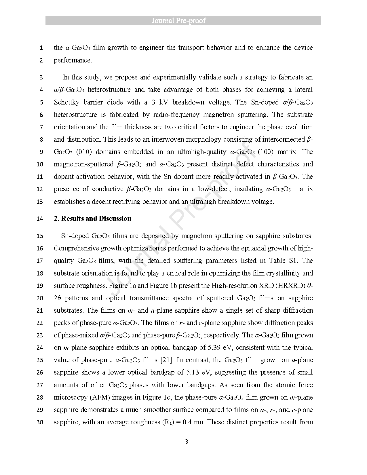
This study demonstrates the use of a hybrid α/β-Ga2O3 phase heterostructure from a strain-relaxed phase transition for carrier transport tuning and high-voltage lateral SBD construction. The α/β-Ga2O3 heterostructure features conductive β-Ga2O3 domains embedded in a heteroepitaxial insulating α-Ga2O3 matrix. This unique heterostructure is realized through strain-relaxed α-to-β Ga2O3 phase transition during the magnetron sputtering growth, where the phase evolution and distribution depend critically on the sapphire substrate orientation and the film thickness. Combined defect and transport characterizations further show that Sn dopants are more readily activated in the β-Ga2O3 phase. The embedded β-Ga2O3 domains in the α/β-Ga2O3 heterostructure show a minor impact on the crystallinity of the pristine α-Ga2O3 matrix but significantly enhance the overall film conductivity. The lateral SBD based on the unique α/β-Ga2O3 heterostructure exhibits a superior breakdown performance compared to the single-phase β-Ga2O3 diode, with a breakdown voltage over 3 kV at 25 °C and over 2 kV at 150 °C.
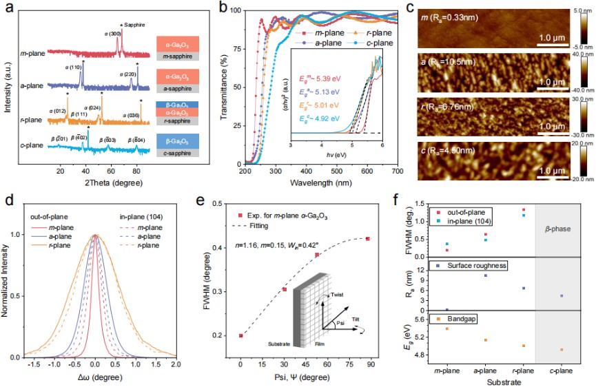
Figure 1. (a) High-resolution XRD patterns for the θ-2θ scans of Ga2O3 films grown on m-, a-, r-, and c-plane sapphire by magnetron sputtering, with a thickness of 150 nm. (b) Optical transmittance spectra of the Ga2O3 films. Inset is the Tauc plots for estimating the direct optical bandgap of the films. (c) AFM images of the Ga2O3 films. (d) XRCs of different planes for Ga2O3 films grown on m-, a-, and r-plane sapphire. (e) XRC FWHM (W) as a function of the inclination angle. The dashed line is a least-squares fit using a model developed by Srikant et al. [26]. The inset is the schematic of the measurement geometry. (f) Plots for comparing XRC FWHM, surface roughness, and bandgap (Eg) in the Ga2O3 films grown on m-, a-, r-, and c-plane sapphire.
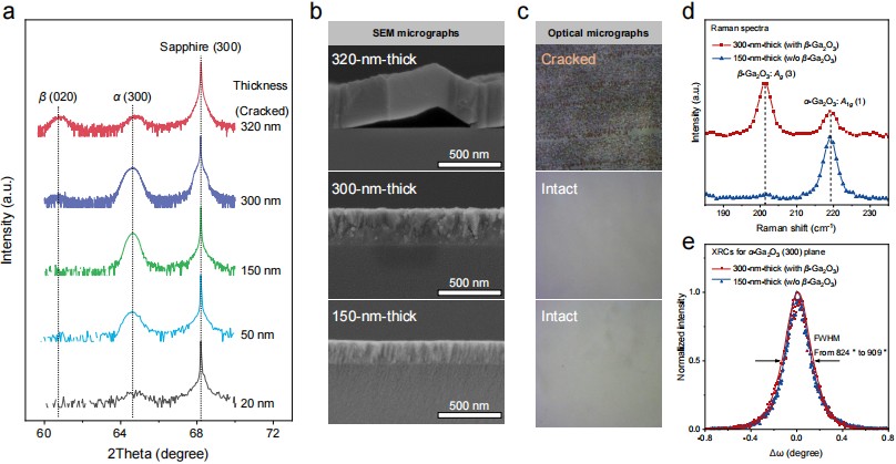
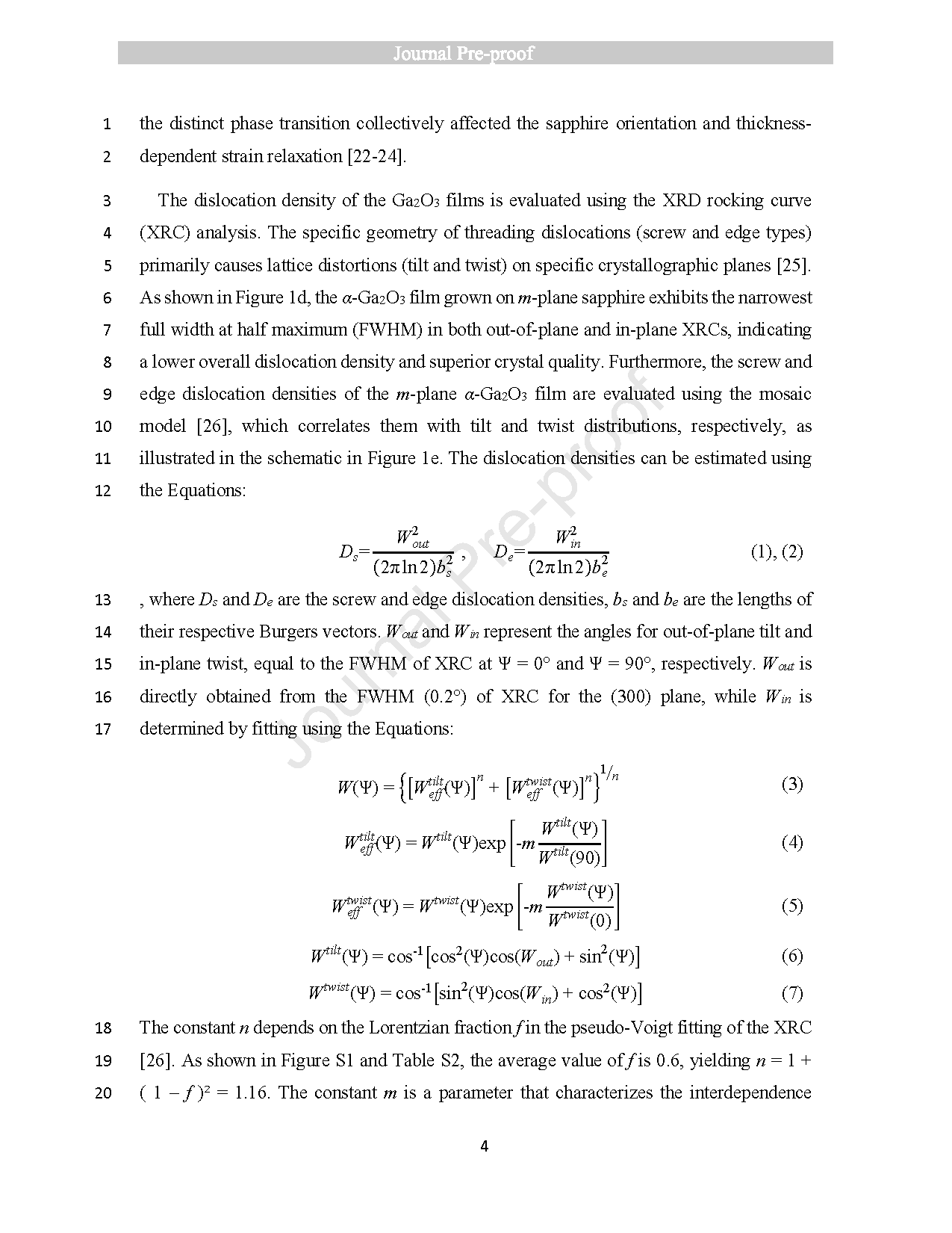
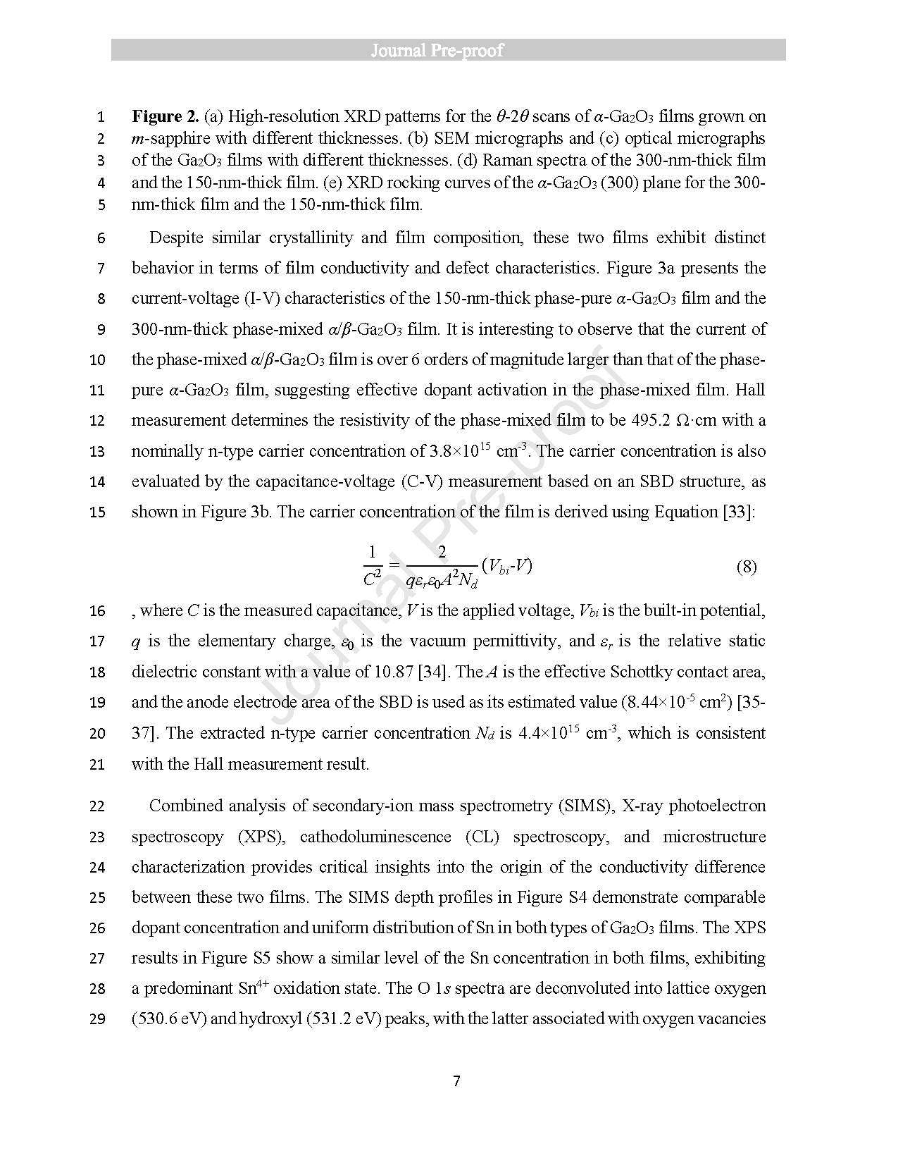
Figure 2. (a) High-resolution XRD patterns for the θ-2θ scans of Ga2O3 films grown on m-sapphire with different thicknesses. (b) SEM micrographs and (c) optical micrographs of the Ga2O3 films with different thicknesses. (d) Raman spectra of the 300-nm-thick film and the 150-nm-thick film. (e) XRD rocking curves of the α-Ga2O3 (300) plane for the 300-nm-thick film and the 150-nm-thick film.
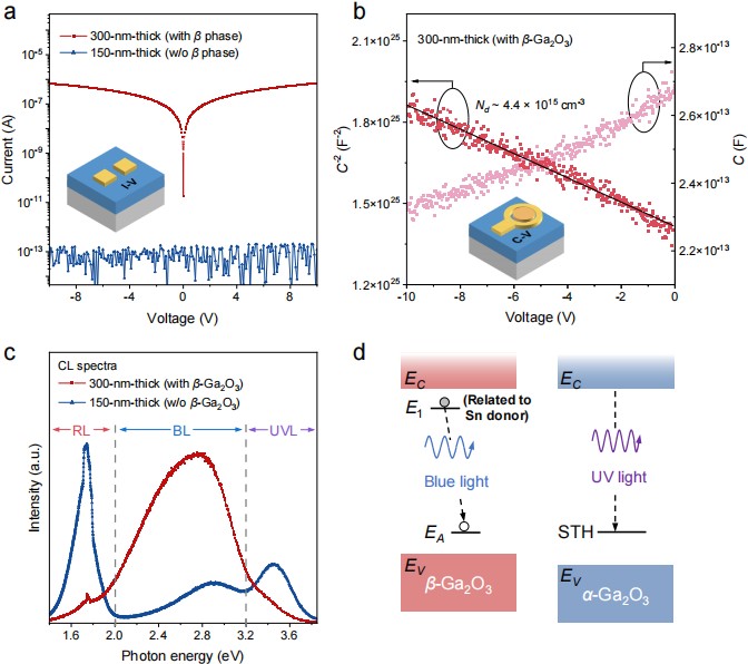
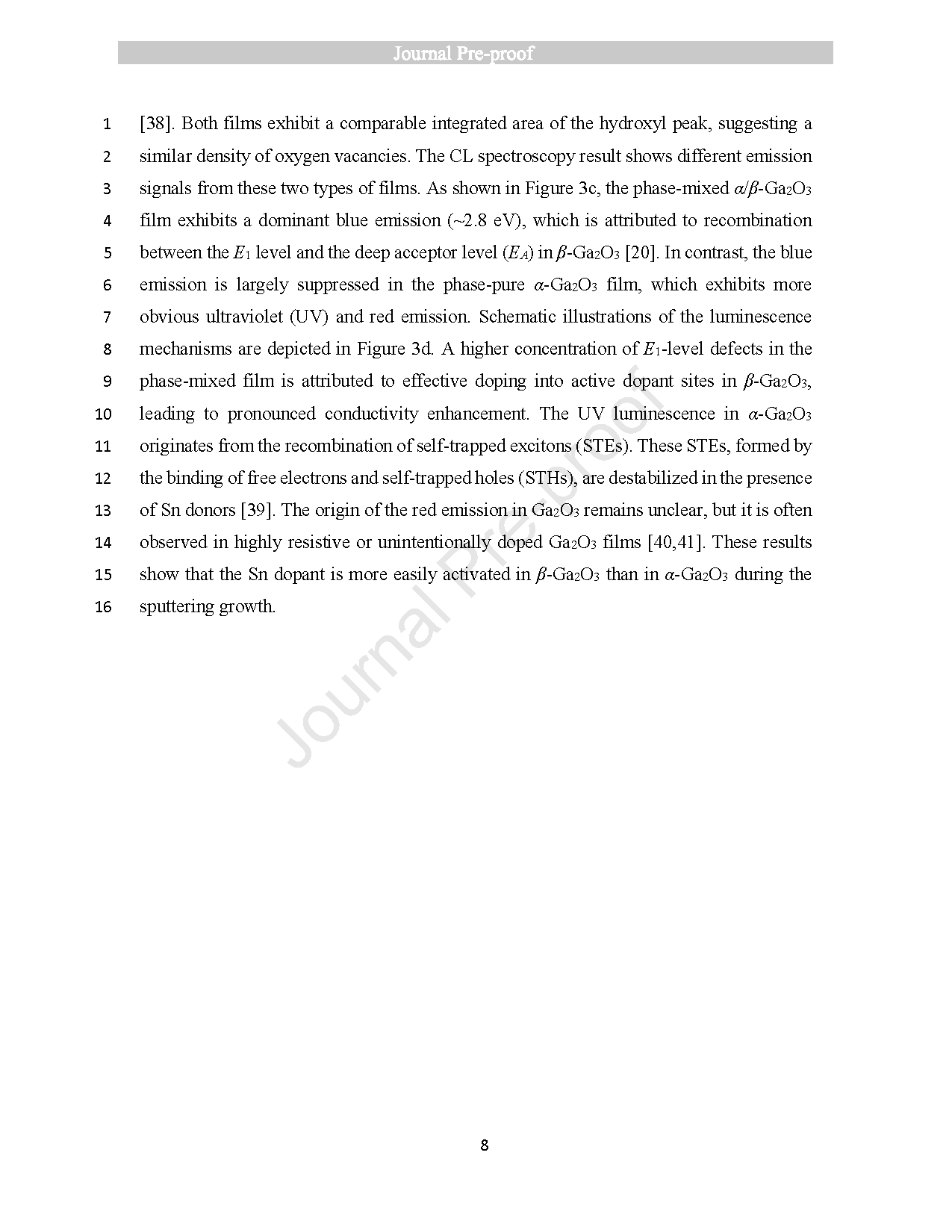
Figure 3. (a) I-V characteristics of the 300-nm-thick phase-mixed α/β-Ga2O3 film and the 150-nm-thick phase-pure α-Ga2O3 film in a planar two-electrode structure. The Ti/Al/Ni/Au metal stacks served as Ohmic contacts with a consistent spacing of 35 μm. (b) C-V characteristics of the 300-nm-thick phase-mixed α/β-Ga2O3 film in a lateral SBD structure. The Ti/Al/Ni/Au and Pt/Au metal stacks as cathode and anode, respectively, with a spacing of 15 μm. (c) CL spectra of the 300-nm-thick phase-mixed α/β-Ga2O3 film and the 150-nm-thick phase-pure α-Ga2O3 film. The spectra are measured at an acceleration voltage of 5 kV. (d) Schematic illustrations depicting the mechanisms of blue light emission from β-Ga2O3 and UV light emission from α-Ga2O3, respectively.
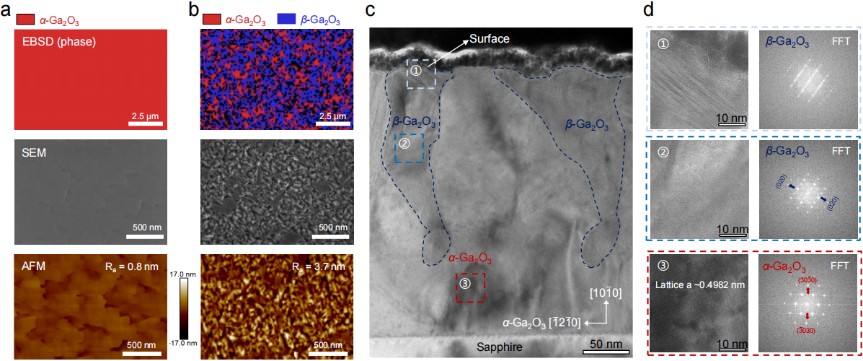
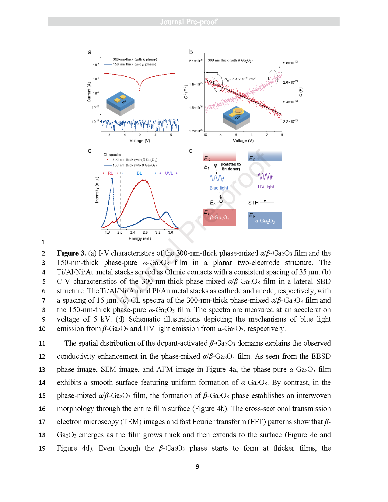
Figure 4. EBSD phase images, SEM images, and AFM images of (a) the 150-nm-thick phase-pure α-Ga2O3 film and (b) the 300-nm-thick phase-mixed α/β-Ga2O3 film, respectively. (c) Cross-section TEM image of 300-nm-thick phase-mixed α/β-Ga2O3 film projected along the [0001] zone axis of α-Ga2O3. (d) Magnified view of the area outlined by the colored rectangle in Figure 4c, with the corresponding FFT patterns.
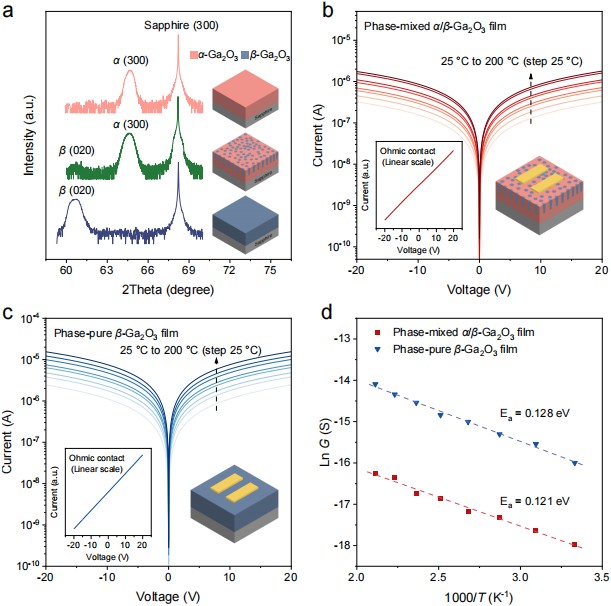
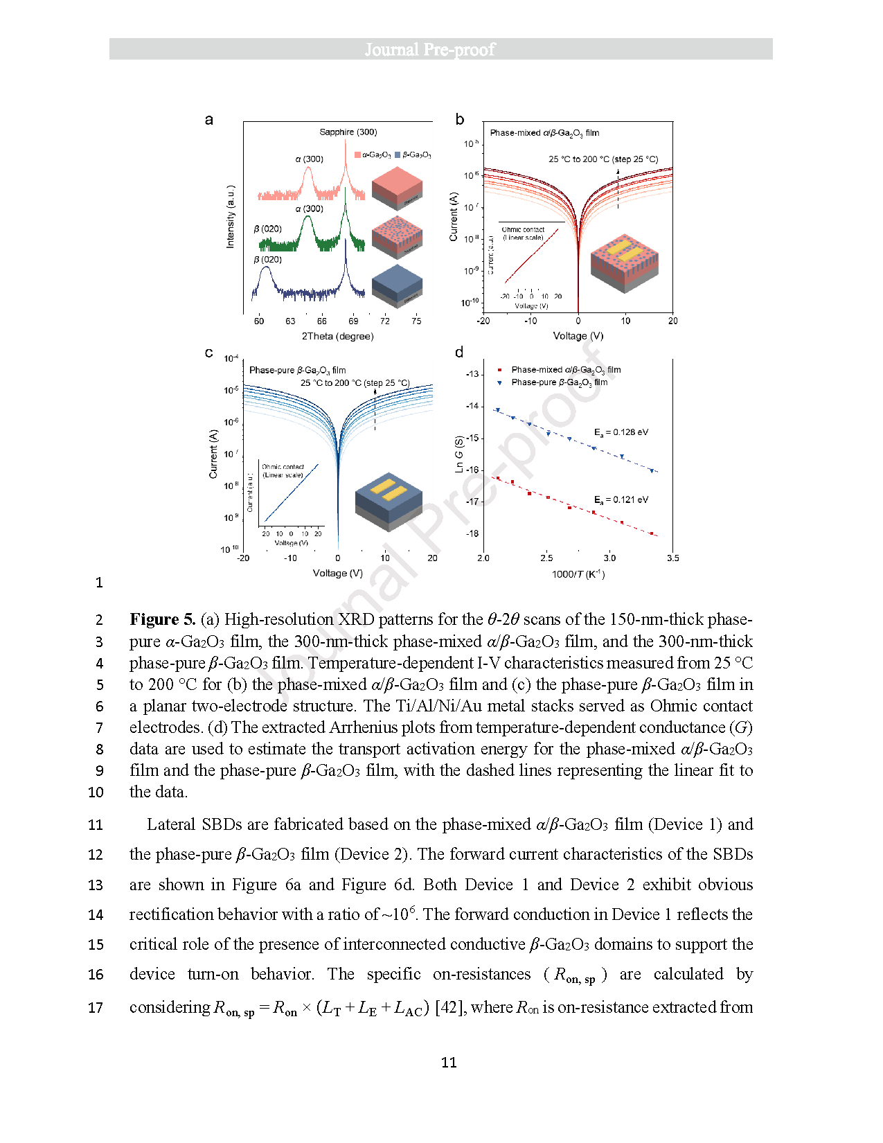
Figure 5. (a) High-resolution XRD patterns for the θ-2θ scans of the 150-nm-thick phase-pure α-Ga2O3 film, the 300-nm-thick phase-mixed α/β-Ga2O3 film, and the 300-nm-thick phase-pure β-Ga2O3 film. Temperature-dependent I-V characteristics measured from 25 °C to 200 °C for (b) the phase-mixed α/β-Ga2O3 film and (c) the phase-pure β-Ga2O3 film in a planar two-electrode structure. The Ti/Al/Ni/Au metal stacks served as Ohmic contact electrodes. (d) The extracted Arrhenius plots from temperature-dependent conductance (G) data are used to estimate the transport activation energy for the phase-mixed α/β-Ga2O3 film and the phase-pure β-Ga2O3 film, with the dashed lines representing the linear fit to the data.
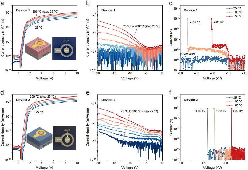
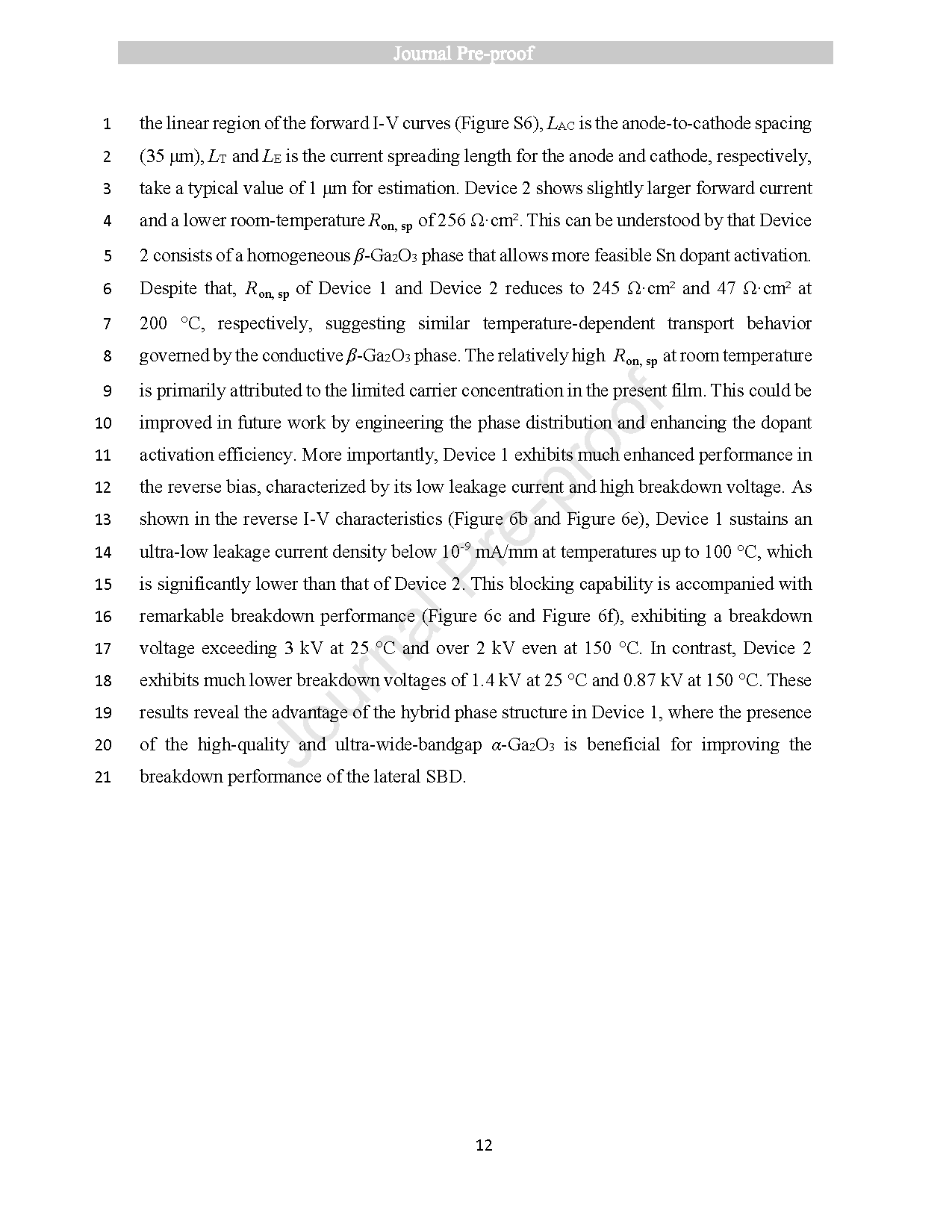
Figure 6. Forward I-V characteristics in a log-scale of (a) Device 1 and (d) Device 2, respectively. The insets are schematic diagrams and top-view optical images of the lateral SBDs. Reverse I-V characteristics in log-scale of (b) Device 1 and (e) Device 2, respectively. The measurements are performed at various temperatures, ranging from 25 °C to 200 °C, with a step-size temperature increment of 25 °C. Reverse breakdown characteristics of (c) Device 1 and (f) Device 2, respectively. The measurements are performed at three different temperatures: 25 °C, 100 °C, and 150 °C.
DOI:
doi.org/10.1016/j.mtphys.2026.102010