


Paper Sharing
【Member Papers】 Overview of Recent Advances in Ga₂O₃ Power Device Research at the Suzhou Institute of Nano-Tech and Nano-Bionics, Chinese Academy of Sciences
日期:2026-01-13阅读:449
01 Background
Gallium Oxide (Ga₂O₃), an ultra-wide bandgap semiconductor, features an exceptionally wide bandgap of 4.8–4.9 eV, an extremely high critical electric field strength (~8 MV/cm), and the potential for large-size, low-cost single-crystal substrates grown via melt-based methods. These advantages make Ga₂O₃ one of the most promising candidates for next-generation power semiconductor devices with ultra-high voltage capability, low power loss, and high cost-effectiveness.
As shown in Figure 1, the fundamental physical properties of β-Ga₂O₃ are compared with those of mainstream semiconductors. To date, Ga₂O₃ power devices have demonstrated outstanding performance metrics at the laboratory level and are expected to enable revolutionary applications in key areas such as tens-of-kilovolt power conversion and transmission, railway traction systems, and energy systems operating under extreme environments.
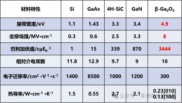
Figure 1 Fundamental physical properties of β-Ga₂O₃ compared with mainstream semiconductors
02 Types and Characteristics of Ga₂O₃ Power Devices
The operating principles of Ga₂O₃ power devices are primarily governed by electric field modulation and carrier transport characteristics, with the ultimate goal of achieving efficient power conversion and control. Currently, the main device structures under active development include Schottky barrier diodes (SBDs), metal–oxide–semiconductor field-effect transistors (MOSFETs), and fin-type power transistors.
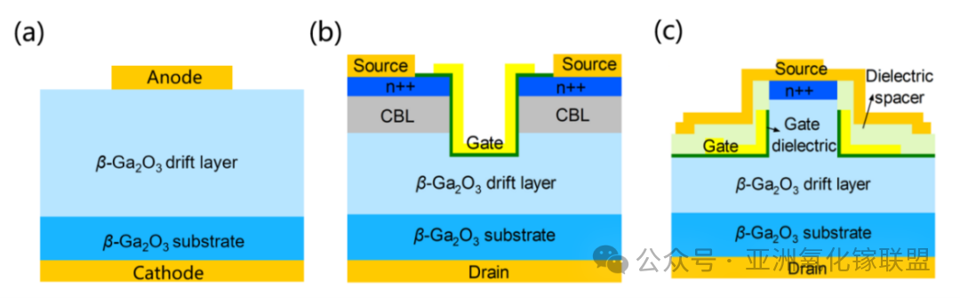
Figure 2 Schematic structures of Ga₂O₃ power devices
Schottky Barrier Diodes (SBDs)
SBDs represent the most mature Ga₂O₃ power devices to date. Their operation is based on unidirectional conduction enabled by the Schottky barrier formed at the metal–semiconductor interface, as illustrated in Figure 2(a). This structure does not require p-type doping, resulting in a relatively simple fabrication process. In addition, SBDs exhibit zero reverse recovery charge, enabling extremely fast switching speeds.
Benefiting from the ultra-high critical electric field of Ga₂O₃, the drift layer can be designed to be extremely thin, leading to an ultra-low theoretical specific on-resistance and significantly reduced conduction losses. However, the main challenge lies in the limited thermal stability of the Schottky barrier height, which causes increased reverse leakage current at elevated temperatures and degrades device reliability. Optimization strategies such as barrier metal engineering and edge termination design are therefore required.
MOSFETs
MOSFETs operate by modulating channel conductivity through gate voltage control, as shown in Figure 2(b). Their key advantage lies in voltage-controlled operation via a gate dielectric, which simplifies driving circuitry and facilitates circuit integration.
However, this device structure faces two fundamental challenges. First, the fabrication of a high-quality gate dielectric interface remains difficult, as the Ga₂O₃/dielectric interface typically contains a high density of defect states, leading to threshold voltage instability and mobility degradation. Second, the intrinsically low thermal conductivity of Ga₂O₃ results in severe self-heating effects, which limit current handling capability and long-term reliability. The development of novel gate dielectric materials and advanced thermal management integration technologies is therefore essential.
Fin-Type Power Transistors
Fin-type power transistors are characterized by fin-shaped vertical channels, as illustrated in Figure 2(c). This structure offers two revolutionary advantages. First, the enhanced electrostatic control provided by the fin geometry effectively suppresses short-channel effects, offering an ideal pathway toward high-performance enhancement-mode (normally-off) devices. Second, higher current density can be achieved by increasing the number of fins, thereby providing larger conductive channels per unit area.
Nevertheless, fabrication of this structure presents significant challenges, particularly the requirement for nanoscale fin etching with smooth, steep sidewalls. In addition, thermal management becomes more complex in three-dimensional device architectures.
Together, these three device structures define the technological roadmap for Ga₂O₃ power devices: SBDs as the first commercially viable rectifier devices with strong potential in high-efficiency rectification; MOSFETs as mainstream switching devices whose interface and thermal challenges must be resolved for industrialization; and fin-type power transistors as an advanced technology direction aimed at higher integration density and superior performance. Their synergistic development will collectively drive the revolutionary application of Ga₂O₃ in ultra-high-voltage and high-efficiency power electronic systems.
03 Team Introduction
Building upon its expertise in third-generation semiconductors, the Nanofabrication Platform has strategically expanded its R&D capabilities and technical infrastructure for ultra-wide bandgap Ga₂O₃ materials and devices. A series of studies on Ga₂O₃ power device fabrication have been carried out, accompanied by the establishment of dedicated testing systems, resulting in the formation of a specialized research team and solid technical foundations.
To date, the team has published more than 20 SCI papers in leading international journals such as Applied Physics Letters and IEEE Electron Device Letters, and has filed over 10 domestic and international invention patents. The Ga₂O₃ R&D team currently consists of 5 senior researchers, 1 postdoctoral fellow, and more than 10 PhD and master’s students.
04 Platform Capabilities and Achievements
The Nanofabrication Platform has successfully developed key process technologies, including high-concentration, high-uniformity nitrogen ion implantation doping and low-damage, high-anisotropy Ga₂O₃ etching. Combined with Ga₂O₃ thin-film epitaxy and thermal processing techniques, these core processes have systematically enhanced the platform’s Ga₂O₃ power device fabrication capabilities, enabling the development of high-performance vertical power diodes and transistors.
High-Concentration, High-Uniformity Nitrogen Ion Implantation Doping
In Ga₂O₃ power devices, achieving high-concentration and precisely controlled selective n-type doping is essential for constructing key regions such as shallow donor source/drain implantation, junction termination structures (e.g., charge balance layers and field rings), gate-underlayer modification, and current blocking layers (CBLs). These doping regions are critical for enhancing breakdown voltage and overall device performance.
Due to the extremely high bond energy and thermal stability of Ga₂O₃, conventional thermal diffusion doping is highly inefficient, making ion implantation the only viable approach for selective doping in Ga₂O₃. This technique faces two major challenges: low activation efficiency after high-temperature annealing, as implanted nitrogen ions struggle to occupy oxygen lattice sites to form acceptors; and severe lattice damage caused by high-energy ion bombardment, which can lead to increased leakage current and reduced reliability if not properly repaired.
To address these challenges, we developed an optimized high-concentration nitrogen ion implantation and high-temperature annealing process. A multi-step energy and dose implantation strategy was employed to form an approximately box-shaped and highly uniform nitrogen doping profile, meeting the stringent requirements of CBL structures. Post-implantation high-temperature annealing in nitrogen or oxygen ambient was identified as a key step for impurity activation and damage recovery, as shown in Figure 3. I–V measurements confirmed that the optimized process enables electron blocking capability on the order of 10⁻⁶ A/cm².
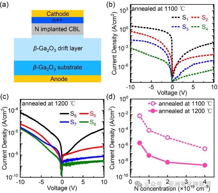
Figure 3 Current blocking capability of CBLs formed under different nitrogen implantation concentrations and annealing conditions
Representative publications:
[1] Z. L. Zuo et al., IEEE Trans. Electron Devices, 2025, vol. 72, no. 5, pp. 2461–2466.
[2] A. J. Luo et al., IEEE WiPDA Asia, Beijing, China, 2025, pp. 1–4.
Low-Damage, High-Anisotropy Ga₂O₃ Etching Technology
Etching is fundamental for defining three-dimensional Ga₂O₃ power device structures such as mesas, trenches, and fins. Device performance—particularly breakdown voltage and dynamic characteristics—is directly related to sidewall morphology, damage level, and smoothness.
We developed a low-damage etching process based on inductively coupled plasma (ICP). By precisely controlling the Cl₂/BCl₃/Ar gas ratio, ICP source power, and RF bias power, high etch rates and strong anisotropy were achieved while minimizing physical bombardment damage. The optimized conditions favor chemically dominated etching mechanisms, resulting in steep, smooth sidewalls. As shown in Figure 4, the etched trenches and fins exhibit near-vertical (~90°) sidewalls and low surface roughness. Post-etch wet surface treatment was further introduced to passivate dangling bonds and restore surface chemical states.
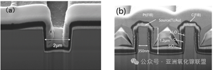
Figure 4 Etching results of Ga₂O₃ U-shaped channels (a) and multi-fin structures (b)
Multi-Fin Channel Ohmic-Contact Anode Diode
The multi-fin channel ohmic-contact anode diode (MFCD) represents a significant breakthrough in the evolution of Ga₂O₃ power diodes toward three-dimensional architectures. The device structure is shown in Figure 5. Its innovation lies in leveraging the self-depletion effect induced by submicron fin channels to form an intrinsic electric-field modulation structure within the device.
This design suppresses reverse leakage current by approximately two orders of magnitude under high electric fields without relying on complex termination structures. By optimizing fin aspect ratio and periodic arrangement, high current density is maintained under forward conduction while preserving low leakage. As shown in Figure 6, the device achieves a forward current density of 400 A/cm² at 5 V. With nitrogen-ion-implanted termination, the reverse breakdown voltage exceeds 1.6 kV, achieving an excellent balance between conduction loss and blocking capability. The fabrication process is highly compatible with conventional planar processes, offering a reliable pathway for next-generation high-voltage, low-loss rectifier development.
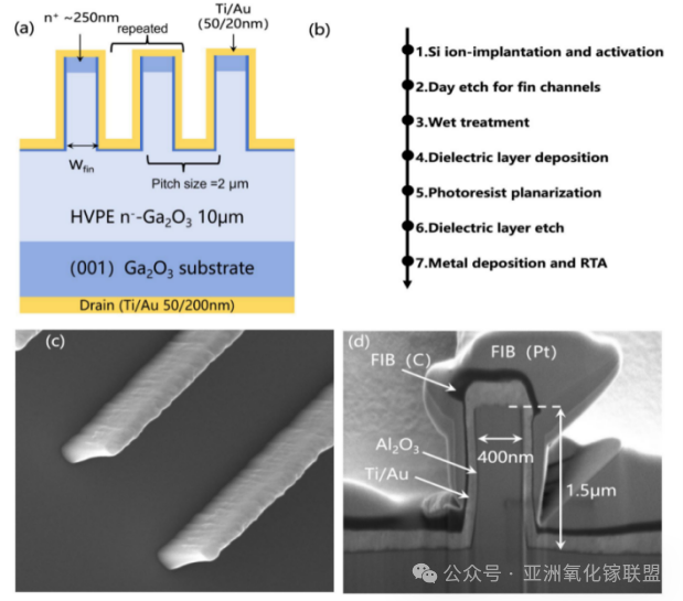
Figure 5. Multi-fin channel ohmic-contact anode diode (MFCD): (a) schematic cross-sectional view of the device, (b) fabrication process flow, (c) SEM image of the etched fin structures, and (d) partial cross-sectional SEM image of the device.
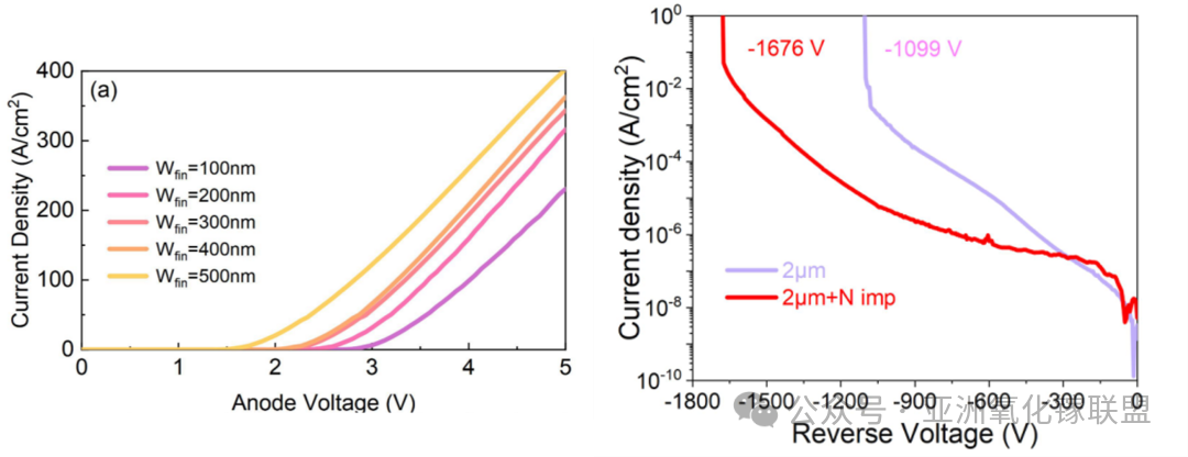
Figure 6. (a) Forward I–V characteristics of MFCDs with different fin dimensions measured by DC sweep in linear scale, and (b) reverse breakdown voltage of MFCDs with N-ion-implanted termination.
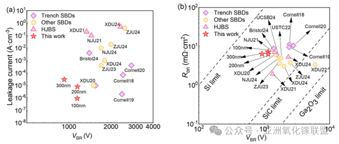
Figure 7. Performance comparison of MFCDs: (a) reverse breakdown voltage versus leakage current, and (b) reverse breakdown voltage versus specific on-resistance.
Representative publications:
[1] G. F. Guo et al., IEEE ISPSD, Japan, 2025, pp. 609–612.
[2] G. F. Guo et al., IEEE IFWS, Xiamen, China, 2025, pp. 1–4.
Vertical Trench MOSFETs
The introduction of nitrogen-ion-implanted current blocking layers effectively addresses key bottlenecks in Ga₂O₃ power switching devices. Device structure, fabrication flow, optical images, and cross-sectional SEM images are shown in Figure 8.
In UMOSFETs, the CBL formed by nitrogen implantation is precisely positioned within the trench region. By co-optimizing implantation concentration (5×10¹⁸ to 4×10¹⁹ cm⁻³) and annealing temperature (1000–1200 °C), vertical electric field distribution is effectively controlled, increasing breakdown voltage from 348 V to 1.3 kV.
However, CBL-based vertical β-Ga₂O₃ UMOSFETs often suffer from increased on-resistance due to deep-level defects on trench sidewalls that trap free electrons. To mitigate this issue, HF sidewall treatment was introduced prior to gate dielectric deposition. This process incorporates fluorine into the sidewall region, increases electron concentration, alleviates compensation effects from deep acceptor states, and partially passivates surface/interface traps while providing mild surface polishing.
As shown in Figure 9, the optimized devices achieved a specific on-resistance of 6.0 mΩ·cm², channel mobility of 19.1 cm²/V·s, and breakdown voltage of 1132 V. These results demonstrate that HF sidewall treatment is an effective surface engineering approach for enhancing the electrical performance of β-Ga₂O₃ UMOSFETs.
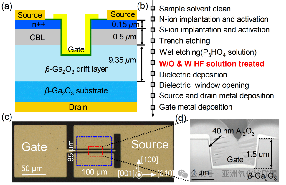
Figure 8. Vertical trench MOSFET: (a) schematic structure, (b) device fabrication process flow, (c) optical image of the fabricated device, and (d) cross-sectional SEM image of the device.
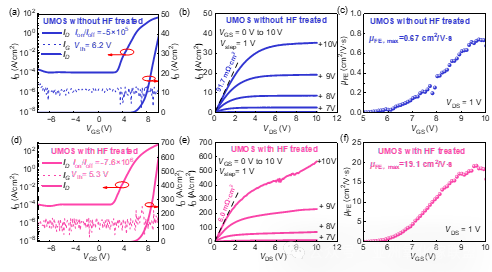
Figure 9. Electrical performance of the vertical trench MOSFETs. Transfer characteristics of UMOSFETs (a) without and (d) with HF solution treatment. Comparison of DC output characteristics of UMOSFETs (b) without and (e) with HF treatment. Field-effect mobility (μ_FE) as a function of gate–source voltage (V_GS) for UMOSFETs (c) without and (f) with HF treatment.
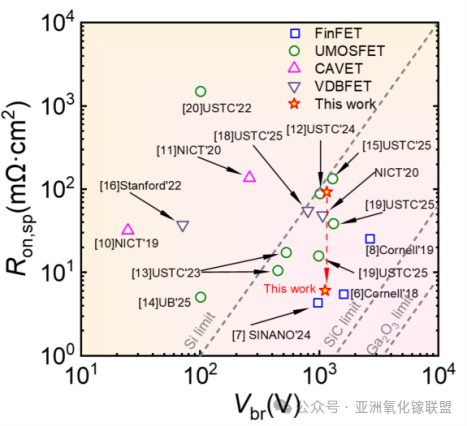
Figure 10. Performance comparison of the fabricated vertical trench MOSFET with other reported devices.
Representative publications:
[1] A. J. Luo et al., Applied Physics Letters, 128, 000000 (2026).
[2] Y. J. Ma et al., IEEE Electron Device Lett., 2023.
[3] Z. L. Zuo et al., IEEE Trans. Electron Devices, 2025.
Vertical Enhancement-Mode Fin-Type Power Transistors
Vertical enhancement-mode fin-type power transistors achieve a breakthrough in Ga₂O₃ power devices through a fully three-dimensional architecture. The devices employ photoresist planarization, non-metal hard-mask etching, and self-aligned processes. Device design and cross-sectional SEM images are shown in Figure 11.
As shown in Figure 12, precise control of fin width and spacing enables complete channel depletion, resulting in a stable threshold voltage of 0.87 V. By integrating multiple fins in parallel, the specific on-resistance is reduced to a record-low 4.3 mΩ·cm², only 1.8 times the theoretical limit. At a breakdown voltage of 975 V, the Baliga figure of merit reaches 0.22 GW/cm².
Comparison with other reported devices (Figure 13) highlights the strong potential of this technology, which lays a solid foundation for the practical application of Ga₂O₃ in tens-of-kilovolt power systems.
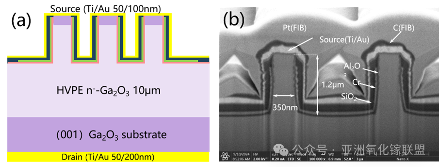
Figure 11. Schematic structure and cross-sectional SEM images of the vertical enhancement-mode multi-fin power transistor.
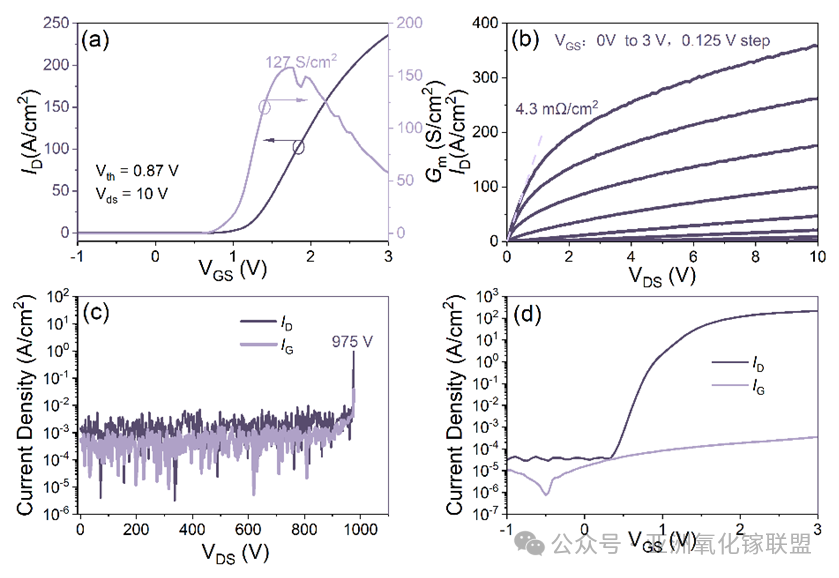
Figure 12. Electrical performance of the vertical enhancement-mode multi-fin power transistor: (a) transfer characteristics and transconductance in linear scale, (b) output characteristics, (c) reverse breakdown characteristics and gate leakage current, and (d) transfer characteristics and transconductance in logarithmic scale.
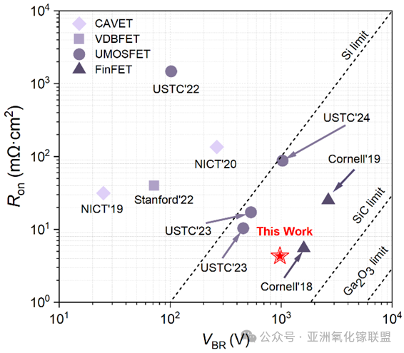
Figure 13. Performance comparison of the vertical enhancement-mode multi-fin power transistor with other reported works.
Representative publication:
[1] G. F. Guo et al., IEEE EDTM, Hong Kong, 2025, pp. 1–3.
