


Member News
【Member News】Good News! Garen Semiconductor Recognized as a High-Tech Enterprise, Adding a New Chapter to Innovation in the Gallium Oxide Field
日期:2026-01-16阅读:580
Recently, Hangzhou Gaen Semiconductor Co., Ltd. (hereinafter “GAREN SEMI”) officially received the High-Tech Enterprise Certificate, jointly approved and issued by the Zhejiang Provincial Department of Economy and Information Technology, the Zhejiang Provincial Department of Finance, and the State Taxation Administration of Zhejiang Province. This authoritative recognition not only affirms the company’s technological innovation capabilities and core competitiveness in the ultra-wide bandgap semiconductor field, but also serves as a strong testament to its deep commitment to Gallium Oxide material research and the promotion of industrial applications, injecting robust momentum into the company’s high-quality development.

The evaluation of high-tech enterprise status rigorously focuses on the innovativeness of core technologies, the intensity of R&D investment, and the ability to translate results into practical applications. Since its establishment, GAREN SEMI has consistently taken technological innovation as its primary driving force, focusing on Gallium Oxide, a core material of the fourth-generation semiconductors. Leveraging a series of original technological breakthroughs, the company has built a solid technological barrier and established a globally leading position in the industry.
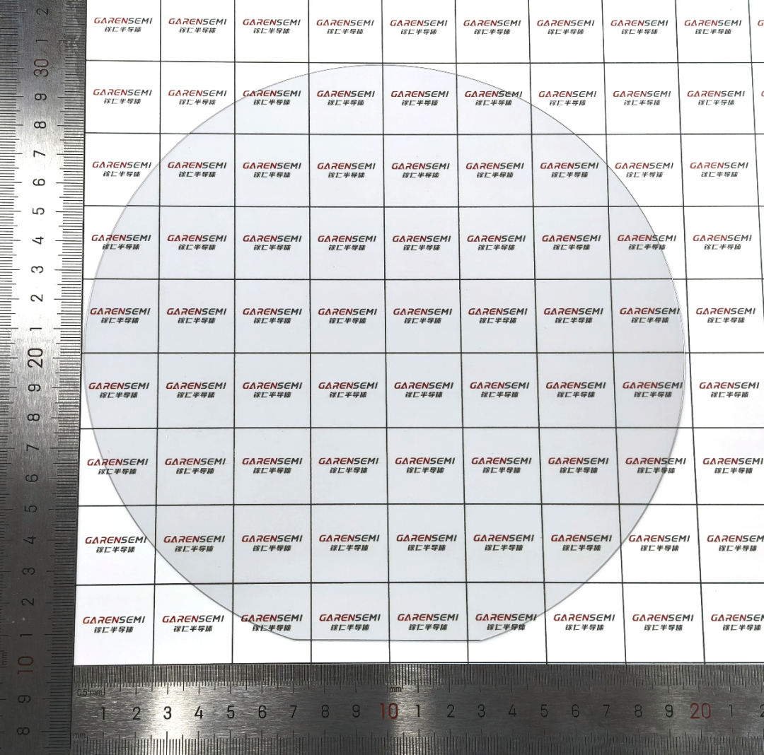
1.Leading multiple technological routes, consolidating Gallium Oxide technology
In core technology development, GAREN SEMI has established a complete Gallium Oxide single-crystal production system, becoming the first company worldwide to achieve multi-route, multi-crystal-plane 8-inch Gallium Oxide single-crystal production:
● Global breakthrough in the Czochralski method: Using its independently developed Czochralski process, the company successfully produced the world’s first 8-inch Gallium Oxide single crystal and substrate. Advantages such as low precious-metal usage, reduced cost, and scalability break foreign monopolies and lay the foundation for domestic substitution.
● Stepwise upgrades of the Vertical Bridgman (VB) method: In 2025, iterative growth of 4-, 6-, and 8-inch single crystals was completed. The 8-inch single crystal reached an isometric length of 20 mm, and the 6-inch (010) plane single crystal achieved over 40 mm, both reaching international leading levels.
● Full-chain layout: The company has successfully realized wafer-level 6-inch off-cut Gallium Oxide substrate preparation, high-quality 6-inch homoepitaxial growth, launched new (011) plane substrates and the “SCIENCE series” research-grade VB long-crystal equipment, forming a complete “equipment–crystal–substrate–epitaxy” product chain.
With these industry-leading achievements, the company has won multiple prestigious awards, including “Top Ten Advances in China’s Third-Generation Semiconductor Technology 2025,” “Major Scientific and Technological Achievement Award 2025” from the Zhejiang Provincial Department of Science and Technology, and the “2024–2025 Semiconductor Materials Industry Contribution Award.” GAREN SEMI holds 13 granted domestic and international invention patents, with more than 50 patents pending, earning authoritative recognition for its technological strength.
2.Broad application prospects, empowering industrial upgrading
As an ultra-wide bandgap semiconductor, Gallium Oxide features a large bandgap, high critical breakdown field, and low energy loss. It holds broad application potential in new energy vehicles, high-voltage power systems, deep-ultraviolet detection, 5G communications, and other fields, contributing to improved energy efficiency and China’s “dual carbon” goals. GAREN SEMI’s 8-inch Gallium Oxide substrates have been verified for superior quality by third-party institutions such as Shenzhen Pinghu Laboratory and Malvern Panalytical Asia-Pacific Center of Excellence, providing core material support for downstream device industrialization.
3.Future plans: targeting leadership and promoting self-reliance
Receiving the high-tech enterprise recognition is both an honor and a responsibility. Moving forward, GAREN SEMI will seize this opportunity to continue increasing R&D investment, focusing on key industrialization stages such as crystal quality improvement, cost optimization, and downstream device validation, accelerating technology iteration and results translation. The company plans to conduct in-depth joint evaluations with downstream device manufacturers to collaboratively verify Gallium Oxide performance in practical scenarios and scale up applications, promoting the construction and rapid development of the domestic Gallium Oxide industry ecosystem.
Additionally, leveraging the Zhejiang Provincial Enterprise Research Institute platform, GAREN SEMI will deepen industry–university–research collaboration with universities and research institutes, attract high-end technical talent, and continue to consolidate its global leadership in Gallium Oxide. The company aims to become a global leader in ultra-wide bandgap semiconductor materials and equipment solutions, contributing core strength to China’s self-reliant semiconductor industry.
About Garen Semiconductor
Founded in September 2022, Hangzhou Garen Semiconductor Co., Ltd. is a technology-driven enterprise specializing in the R&D, production, and sales of wide-bandgap semiconductor materials such as Gallium Oxide. Leveraging the State Key Laboratory of Silicon and Advanced Semiconductor Materials at Zhejiang University and the Zhejiang University Hangzhou International Science and Innovation Center, the company has built a strong R&D, production, and operations team led by an academician of the Chinese Academy of Sciences as chief advisor.
Garen Semiconductor has pioneered new Gallium Oxide single-crystal growth technologies and has secured 14 international and domestic invention patents, breaking Western monopolies and technological blockades in Gallium Oxide substrate materials. Oriented toward addressing major national needs, the company is committed to sustained innovation in the upstream Gallium Oxide industry chain, striving to provide reliable material support for China’s power electronics and related industries.
By leading industry innovation, Garen Semiconductor has adopted proprietary casting and other novel single-crystal growth technologies to achieve breakthroughs in the production of 8-inch Gallium Oxide single-crystal substrates and wafer-scale (010)-oriented single-crystal substrates. The company has also developed the first Gallium Oxide–dedicated VB crystal growth system with an integrated process package. Garen Semiconductor has mastered core technologies across the entire Gallium Oxide value chain—including crystal growth, processing, and epitaxy—and provides customers with large-size, high-quality Gallium Oxide products and equipment backed by fully independent intellectual property rights.
For more information about GAREN SEMI and its products
Visit our official website: http://garen.cc/
Or contact us in the following ways:
Mr. Jiang :15918719807
Email :jiangjiwei@garen.cc
Mr. Xia :19011278792
Email :xianing@garen.cc
