


Member News
【Member News】Breaking a 20-Year Technology Stalemate! Xidian University Team Overcomes Global Challenge in Chip Heat Dissipation
日期:2026-01-16阅读:503
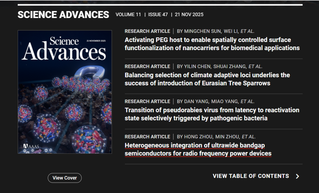
For a long time, the semiconductor industry has faced a fundamental paradox: we know that the next-generation materials will have superior performance, yet we often do not know how to manufacture them. “It’s like knowing how to control the heat, but truly mastering it is extremely difficult,” said Zhou Hong, using this analogy. Recently, a team led by Academician Hao Yue and Professor Zhang Jincheng achieved a historic breakthrough in this core challenge. By transforming the “island-like” connections between materials into atomically flat “films,” they dramatically enhanced both the heat dissipation efficiency and overall performance of chips. This achievement not only breaks a nearly 20-year technological stalemate but also demonstrates enormous potential in frontier technologies. The results have been published in top international journals Nature Communications and Science Advances, with the latter featuring the work as a cover article.
From “Rough Islands” to “Smooth Highways”: A Paradigm-Shifting Process Revolution
In semiconductor devices, the quality of interfaces between different material layers directly determines overall performance. This is especially true for third-generation semiconductors represented by GaN and fourth-generation semiconductors represented by Ga₂O₃. A key challenge is how to integrate these materials efficiently and reliably. Traditional methods use aluminum nitride (AlN) as an intermediate “adhesive layer,” but during growth, the adhesive layer spontaneously forms countless irregular, uneven “islands.” “It’s like building canals on a rugged dam,” Zhou Hong explained. “The island-like structures create severe resistance for heat transfer across interfaces, forming ‘thermal bottlenecks.’” Heat accumulation inside the chip can degrade performance or even damage the device. Since the relevant nucleation technology received a Nobel Prize in 2014, this problem has remained unsolved, severely limiting the power enhancement of RF chips.
The team’s breakthrough lies in fundamentally changing the growth mode of the AlN layer. They innovatively developed an “ion-implantation-induced nucleation” technique, transforming the previously random and uneven growth process into a precise and controllable uniform growth. “It’s like turning random sowing into planned, evenly spaced planting, eventually producing a neat, uniform crop,” Zhou described. This process transforms the AlN layer from a rough, polycrystalline “island-like” structure into a single-crystal film with highly ordered atomic arrangements.

This transition brings a qualitative leap: the flat single-crystal film significantly reduces interface defects, allowing heat to rapidly transfer through the buffer/nucleation layer. Experiments show that the interface thermal resistance of the new structure is only one-third that of the traditional island-like structure. This seemingly fundamental materials innovation directly addresses the common heat dissipation challenge faced by both third- and fourth-generation semiconductors, laying the most critical foundation for subsequent performance breakthroughs.
Performance Leap of 40%: From Lab Data to Broad Application Prospects
The process innovation directly translates into remarkable device performance. Using this AlN thin-film technology, the team fabricated GaN microwave power devices achieving output power densities of 42 W/mm in the X-band and 20 W/mm in the Ka-band, boosting international performance records by 30–40%—the largest breakthrough in nearly two decades. “This means that for the same chip area, detection range can be significantly increased, and for communication base stations, signal coverage can extend farther with lower energy consumption,” Zhou Hong said. For consumers, the benefits will gradually appear. Although civilian devices like smartphones currently do not require such high power density, advances in foundational technology are broadly beneficial. “In the future, mobile phones may receive stronger signals in remote areas, and battery life could be longer.” More broadly, this technology lays the groundwork for 5G/6G communications, satellite internet, and other future industries by providing key core device capabilities.
Future Vision: A New Research Paradigm Opens Pathways in Semiconductors
The long-term impact of this work extends beyond record-breaking performance numbers. Its core value lies in transforming AlN from a specific “adhesive” into a versatile, scalable “universal integration platform,” offering a replicable model for high-quality integration of various semiconductor materials. “Our work provides a standard solution to the fundamental question of how to perfectly combine two different materials,” Zhou Hong emphasized. The team is already looking further ahead. While AlN is excellent, ultimate materials with even higher thermal conductivity, such as diamond, could further enhance device power handling by an order of magnitude or more—potentially ten times higher. Achieving this, however, will require another cycle of long-term research, possibly spanning a decade.
This relentless pursuit of material limits is the core driver of continuous semiconductor advancement. From the initial explorations by Hao Yue’s team in the late 1990s to today’s consolidated breakthrough, this achievement embodies over 20 years of persistent research. It vividly demonstrates that in hard-tech fields like chips, translating theory into practical applications requires long-term, focused foundational research.
The success of this study marks a crucial leap for China from following to competing and leading in semiconductor frontier technologies, providing a new Chinese model for global semiconductor progress. In practical terms, it means that navigation signals remain stable during mountain drives, smartphones no longer lag due to overheating, and electric vehicle range improves thanks to more efficient chips. Behind these seemingly small improvements lies progress in material-level technology. As this universal technique matures and spreads, it will further consolidate China’s advantages in third-generation semiconductors, accelerate the practical adoption of fourth-generation semiconductors, and inject powerful momentum into securing national information technology security and seizing future technological high ground.
