


Alliance News
【Alliance News】2025 China's Gallium Oxide Industry: Coordinated Efforts Driving Comprehensive Advancement
日期:2026-01-28阅读:1413
Introduction
In 2025, China’s Gallium Oxide industry continued to advance steadily while accumulating experience. Progress unfolded across multiple layers—from material preparation to device exploration, from scientific research breakthroughs to industrial collaboration. Drawing on the alliance platform’s long-term monitoring and aggregation of industry developments, it is evident that multiple forces, led by alliance member companies, are actively advancing within their respective tracks, steadily strengthening the domestic industrial ecosystem.
This report provides a staged overview of the domestic Gallium Oxide industry based on the alliance’s published and continuously tracked information. By summarizing company deployments, technological advancements, and collaborative initiatives, it outlines the overall landscape of coordinated development in China’s Gallium Oxide industry, highlighting its gradually forming industrial rhythm and growth potential. (The following news items are presented in the order in which member units—directors and members—joined the alliance.)
Fujia Gallium: Accelerating the Full-Chain Industrialization of Gallium Oxide
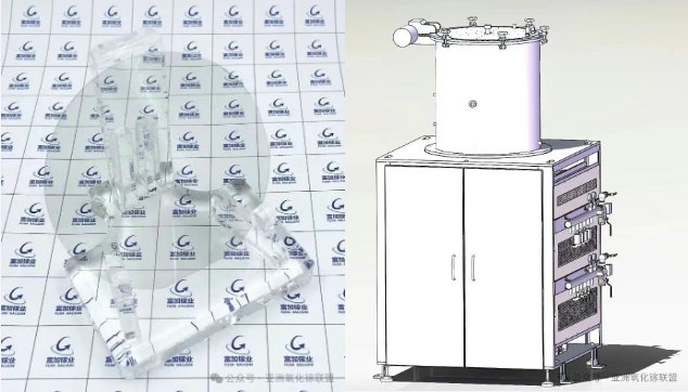
In February 2025, Fujia Gallium achieved stable growth of 4-inch Gallium Oxide single crystals using the vertical Bridgman (VB) method, with substrate quality reaching international advanced standards. Simultaneously, the company launched its self-developed VB growth equipment and process package, advancing the preparation of Gallium Oxide crystals toward engineering applications.
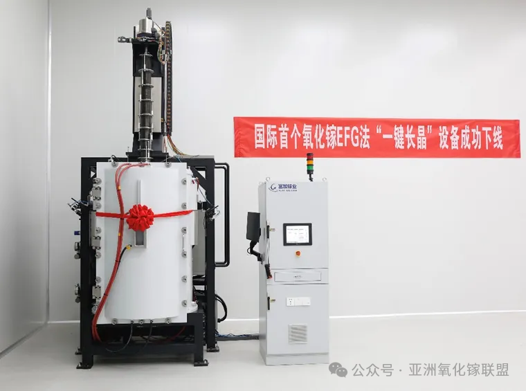
In May 2025, Fujia Gallium completed the on-site acceptance and commissioning of the Gallium Oxide EFG method “one-click crystal growth” equipment, extending single-crystal growth from a technological breakthrough to automated and engineering applications.
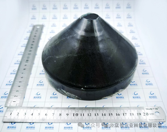
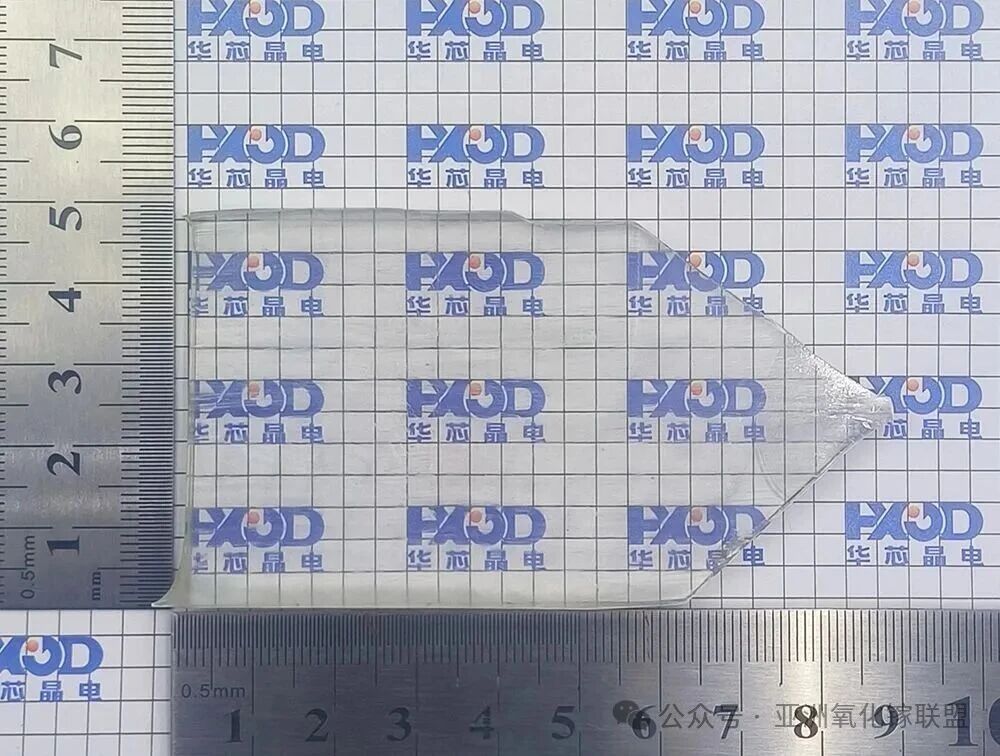
In September 2025, Fujia Gallium made a major breakthrough in Gallium Oxide crystal growth—successfully producing a 6-inch Gallium Oxide single-crystal ingot domestically for the first time using the vertical Bridgman (VB) method. The crystal’s equiaxed height reached 30 mm, suitable as conductive material for power devices, meeting the processing requirements of complete 6-inch Gallium Oxide conductive substrates. The related crystal dimensions and equipment capabilities achieved phased expansion.
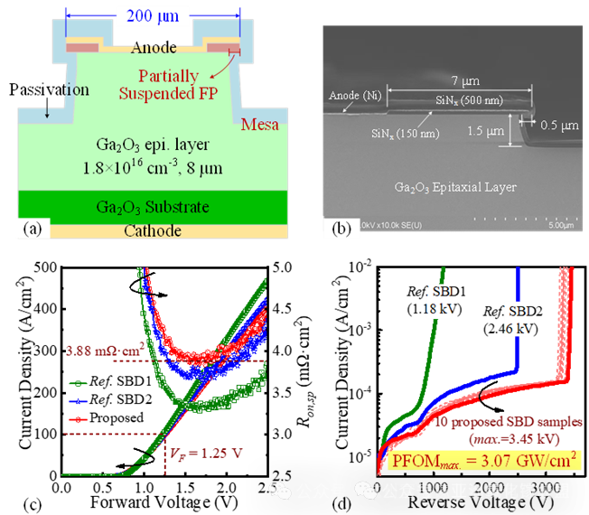
In October 2025, based on Fujia Gallium’s MOCVD Gallium Oxide epitaxial wafers, Fuzhou University achieved internationally leading performance in vertical power Schottky diodes. At the same time, Fujia Gallium made new progress in homogeneous Gallium Oxide MOCVD epitaxy. According to authoritative tests, the mobility of its thick epitaxial wafers reached 181.6 cm²/V·s, and the corresponding 6-inch wafers have entered the device fabrication stage. Fujia Gallium will provide high-quality Gallium Oxide epitaxial wafers to downstream research and industrial users, supporting the full-chain development of high-performance Gallium Oxide power devices in China.
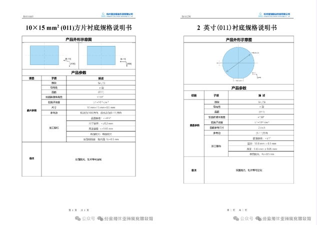
Also in October, Fujia Gallium officially launched new (011) Gallium Oxide substrates, covering small pieces and 2-inch standard specifications, and fully opened customization services for 4-inch substrates and 2–4-inch epitaxial wafers. This enriched the company’s Gallium Oxide substrate and epitaxial product portfolio, providing key material solutions for high-voltage power devices and other high-end applications.
In November 2025, Fujia Gallium formally reached a global strategic cooperation with German epitaxy company NextGO Epi. This collaboration combines Fujia Gallium’s accumulated capabilities in Gallium Oxide crystal growth and full-chain manufacturing with NextGO Epi’s expertise in high-quality epitaxial materials, reflecting a trend of Sino-European synergy in Gallium Oxide materials and industrial processes.
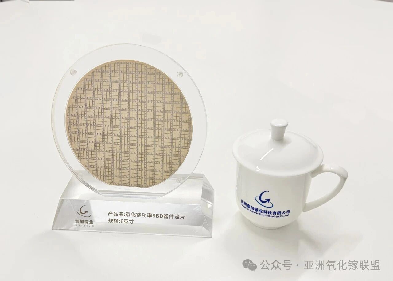
Also in November, at APCSCRM 2025, Fujia Gallium released 6-inch vertical Gallium Oxide SBD wafers. These wafers, fabricated using the company’s self-developed high-mobility homogeneous Gallium Oxide epitaxial wafers, demonstrate the further realization of synergy in Gallium Oxide materials, epitaxy, and devices, and indicate that Gallium Oxide is gradually entering the stage of large-scale device verification.
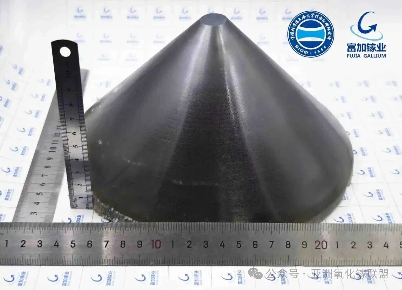
In December 2025, the Shanghai Institute of Optics and Fine Mechanics of the Chinese Academy of Sciences, in collaboration with Fujia Gallium, successfully produced 8-inch Gallium Oxide crystals for the first time internationally using the vertical Bridgman (VB) method, setting a new record for VB-method Gallium Oxide crystal size. This achievement marks continued breakthroughs in Gallium Oxide crystal size and preparation processes, laying a foundation for high-voltage power devices and large-scale industrial applications.
Throughout 2025, Fujia Gallium continued to strengthen its downstream presence in the Gallium Oxide industrial chain, achieving multiple key breakthroughs from epitaxial materials to device applications. The company successfully launched high-mobility MOCVD homogeneous epitaxial wafers and verified the internationally leading performance of vertical power Schottky diodes based on these wafers. Meanwhile, the preparation of 6-inch and 8-inch VB-method Gallium Oxide single crystals provides reliable support for large-scale device fabrication. Through collaboration with downstream research institutions and industrial partners, as well as international strategic partnerships, Fujia Gallium has accelerated the engineering application of Gallium Oxide materials in power electronic devices, solidifying its leading position at the industrial application end of the supply chain.
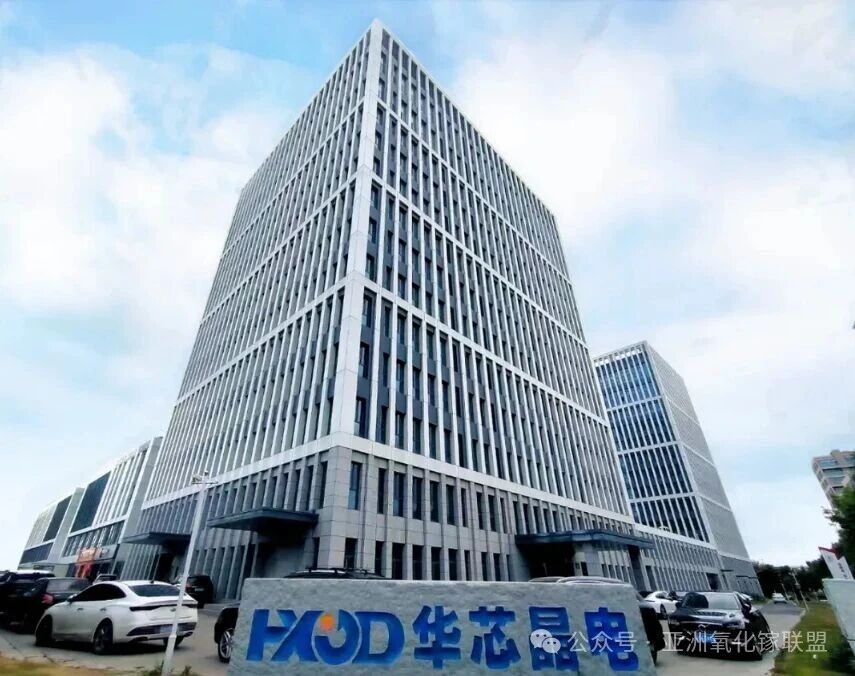
GAO Semiconductor: Full-Chain Layout and Industrialization of Gallium Oxide
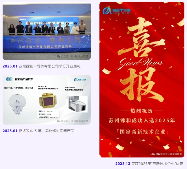
In January 2025, GAO Semiconductor Co., Ltd. officially opened in Xinshengli, Suzhou Industrial Park. During the opening ceremony, the company showcased its technological and production capabilities in Gallium Oxide single-crystal substrates, epitaxial wafers, high-sensitivity solar-blind UV detectors, high-power power electronic devices, and dedicated crystal growth equipment design and manufacturing. Several industrial chain cooperation agreements were also signed, highlighting the company’s leading position in the Gallium Oxide industry layout.
At the event, GAO Semiconductor officially launched key products and equipment, including 6-inch Gallium Oxide substrates, solar-blind UV focal plane imaging chips, and corona discharge real-time monitoring devices. These launches marked a significant step in the industrialization of Gallium Oxide materials and devices. The new products offer high-quality large-size substrates, customizable epitaxial wafers, and end-use device capabilities, providing strong support for high-power semiconductor devices and high-sensitivity UV detection applications. They also demonstrate the company’s engineering capabilities in promoting the full-chain industrialization of Gallium Oxide.
In December 2025, GAO Semiconductor was included in the first batch of high-tech enterprise filings in Jiangsu Province and officially received national high-tech enterprise certification, showcasing the company’s innovation strength and industry influence in Gallium Oxide technology R&D and industrialization.
Throughout 2025, GAO Semiconductor completed its opening and operational launch, released 6-inch Gallium Oxide substrates and core devices, and received high-tech enterprise recognition. This demonstrates that the company is accelerating the transition from laboratory research to full-chain engineering implementation, establishing a solid competitive foundation in the Gallium Oxide sector.
GAREN Semiconductor: Leading New Heights in Gallium Oxide Single-Crystal and Epitaxial Technology
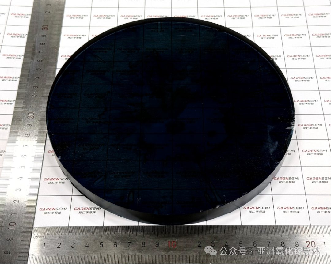
In March 2025, GAREN Semiconductor successfully fabricated the world’s first 8-inch Gallium Oxide single crystal and processed the corresponding wafer substrates, setting a record for the annual upgrade in Gallium Oxide single-crystal size. This breakthrough not only ushered China’s Gallium Oxide industry into the 8-inch era but also laid the foundation for industrial applications, improved production efficiency, and enhanced global competitiveness.
In May 2025, GAREN Semiconductor signed a global strategic cooperation agreement with Germany’s NextGO.Epi. Leveraging their technological advantages, both parties will collaboratively advance research and industrialization of the ultra-wide bandgap semiconductor material Gallium Oxide, jointly promoting breakthroughs in applications within new energy and power electronics, injecting new momentum into the global semiconductor industry.
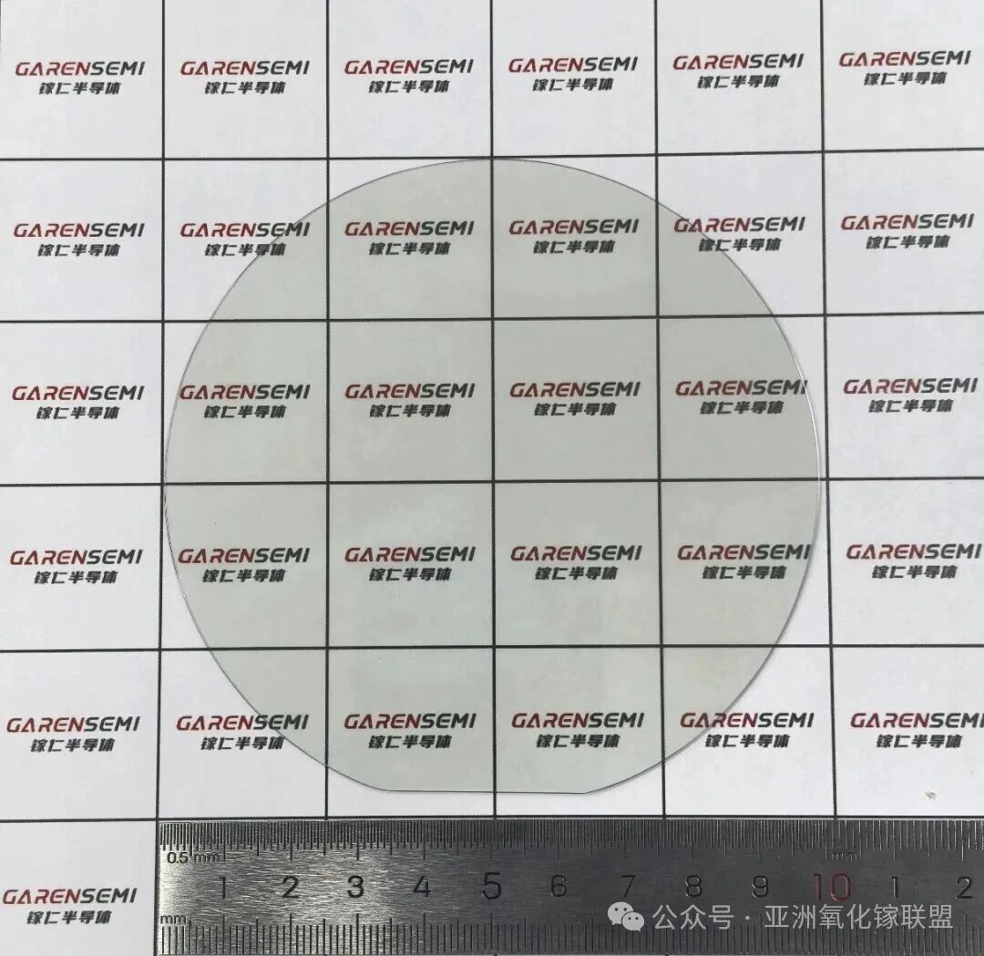
In June 2025, GAREN Semiconductor achieved a breakthrough in large-size Gallium Oxide crystal growth and substrate processing, successfully fabricating 100 mm (010) Gallium Oxide single-crystal substrates using self-developed VB-method equipment. Characterization testing showed the substrates were twin-free, with XRD FWHM less than 50 arcsec and surface roughness below 0.1 nm, reaching internationally advanced standards. This marked the first international report of Gallium Oxide substrates of this size.
In September 2025, GAREN Semiconductor made a major breakthrough in epitaxial technology, successfully achieving high-quality 6-inch Gallium Oxide homoepitaxial growth, representing a milestone in the company’s development.
In October 2025, GAREN Semiconductor achieved another breakthrough in crystal growth technology. Using self-developed Gallium Oxide dedicated crystal growth equipment and the vertical Bridgman (VB) method, the company successfully grew 6-inch (010) Gallium Oxide crystals, with an equal-diameter section exceeding 40 mm, reaching internationally leading levels.
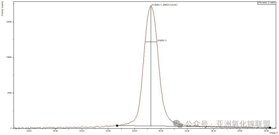
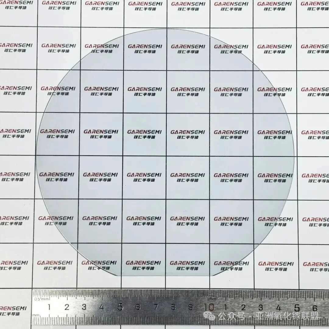
In November 2025, GAREN Semiconductor launched new (011) Gallium Oxide substrate wafers, providing core support for high-power device R&D. These wafers feature precise dimensions, stable crystal orientation, XRD FWHM of only 32.1 arc sec, peak positions close to theoretical values, ultra-smooth surfaces (Ra <0.5 nm), and deviation controlled within ±1°, while offering multiple doping and carrier concentration options to meet diverse device design needs.
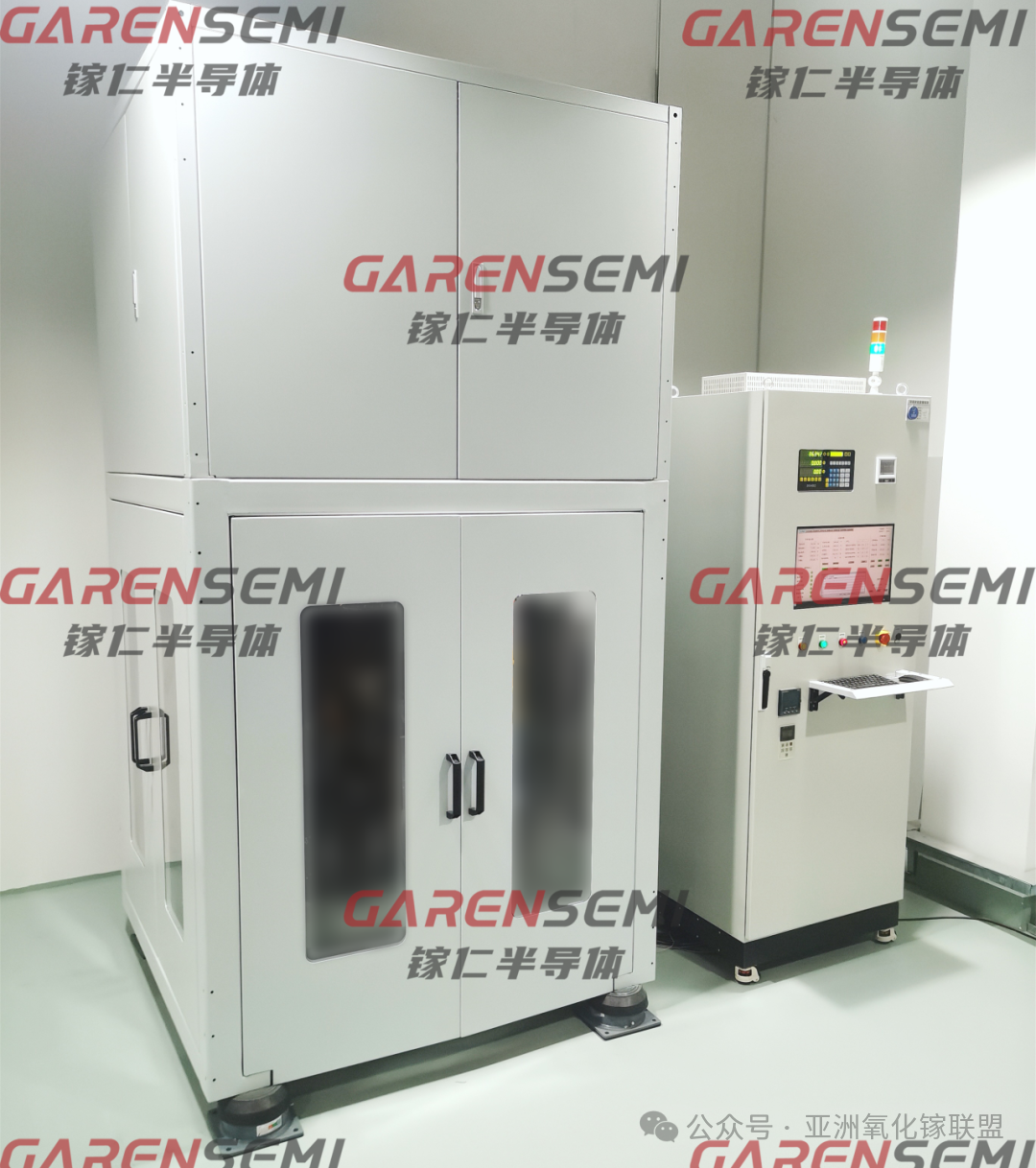
In December 2025, GAREN Semiconductor Co., Ltd. officially launched the “SCIENCE Series” research-grade VB-method crystal growth equipment, tailored for 2–6-inch Gallium Oxide research scenarios. With fully independent core technology, it supports researchers in efficiently exploring crystal growth, doping, defect control, and material performance optimization.
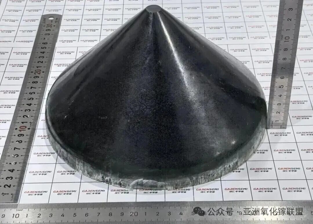
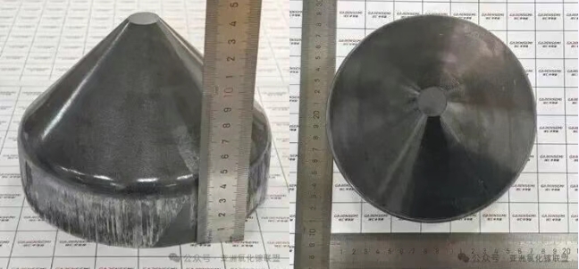
Also in December, GAREN Semiconductor successfully grew 8-inch Gallium Oxide single crystals using the vertical Bridgman (VB) method, achieving an 8-inch equal-diameter length of 20 mm. As the world’s first company to produce 8-inch Gallium Oxide single crystals across multiple technical routes and crystal planes, GAREN Semiconductor has established itself as a global leader in Gallium Oxide materials through a series of original technological breakthroughs.
Throughout 2025, GAREN Semiconductor achieved a series of breakthroughs in Gallium Oxide single-crystal and epitaxial technologies, steadily upgrading from 100 mm substrates to 8-inch single crystals. This marks significant growth in the company’s capabilities in crystal growth, substrate processing, and epitaxial fabrication. Meanwhile, the company launched multiple high-performance substrate wafers and research-grade crystal growth equipment to support high-power device R&D and scientific exploration. Through global strategic cooperation, it promoted the application of Gallium Oxide materials in new energy, power electronics, and other fields. The year’s achievements highlight GAREN Semiconductor’s technological leadership and industrial pioneering position in the global Gallium Oxide sector.
Fujian Sunwise Semiconductor: Continuously Advancing Gallium Oxide High-Frequency Filter Chip Production Line
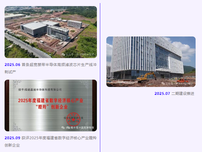
In June 2025, the Phase II project of Fujian Sunwise Semiconductor was accelerating construction, aiming to establish the world’s first Gallium Oxide piezoelectric thin-film high-frequency filter chip production line, with an annual output of 400 kk. This project filled a domestic gap and promoted the development of local new materials industry.
In July 2025, construction of this Gallium Oxide piezoelectric thin-film high-frequency filter chip production line proceeded smoothly, with the main project building fully topped out.
In September 2025, Sunwise Semiconductor, leveraging its fully independent intellectual property core technologies, was again recognized, earning the “Fujian Province Core Digital Economy Industry Gazelle Innovation Enterprise” award for the third consecutive year.
Throughout 2025, Fujian Sunwise Semiconductor, relying on its proprietary core technologies and innovative capabilities, solidified its leading position in the global Gallium Oxide piezoelectric thin-film sector. The company not only established comprehensive competitiveness in key materials and core devices but also became an important pillar in China’s ultra-wide bandgap semiconductor industry chain. With accumulated technical expertise and industrialization capability, Sunwise promoted the development of 5G and high-frequency power electronic devices while further establishing a strategic position in the international frontier materials field.
Guangzhou Tanoxi Technology: First Production Plant in Nansha Launched, Empowering the Bay Area Semiconductor Material Cluster
In May 2025, Tanoxi Technologyachieved a key leap from laboratory research to industrialization, officially putting its first advanced production plant in Guangzhou Nansha into operation, capable of batch Gallium Oxide epitaxial production. As the only global enterprise to stably realize p-type conductive Gallium Oxide epitaxy, Tanoxi not only filled a long-standing material system gap but also laid the foundation for building Gallium Oxide bipolar devices, greatly expanding its application potential in new energy vehicles, industrial robotics, and high-voltage power electronics. This also established an important domestic technology platform for the industrialization of fourth-generation semiconductors.
Jingsheng Electronic Technology: Expanded Factory Officially Operational, Opening a New Chapter of Development

In November 2025, Jingsheng Electronic Technology Co., Ltd. officially put its newly expanded factory into operation, accelerating the production of high-end equipment related to Gallium Oxide and other third- and fourth-generation semiconductor materials. The new facility is equipped with advanced machinery and intelligent management systems, optimizing production processes and significantly enhancing capacity and efficiency.
This expansion not only consolidates the company’s technological and market position in the high-end semiconductor equipment sector but also provides strong support for the application and promotion of Gallium Oxide materials, the improvement of the industry chain, and local economic development.
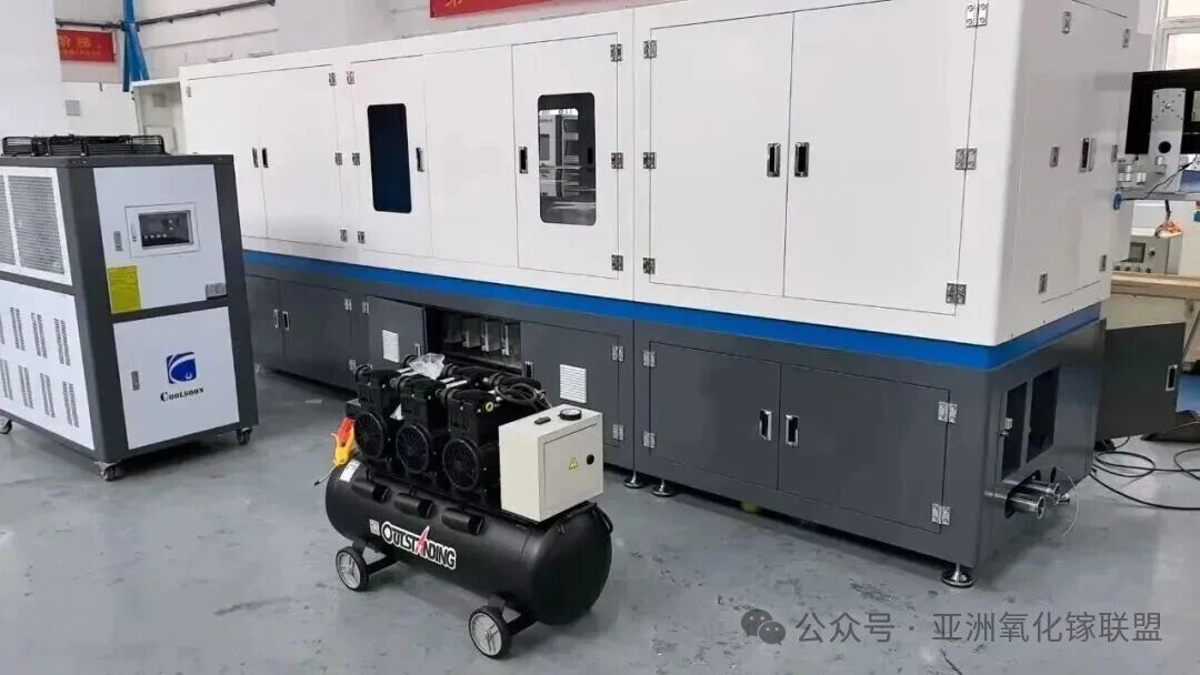
Shenzhen Pinghu Laboratory: Independently Designed Comprehensive Characterization System for Ultra-Wide Bandgap Semiconductor Materials and Devices Fills Industry Gap
In May 2025, Shenzhen Pinghu Laboratory established a complete system for material growth, device fabrication, theoretical modeling, and performance testing. The laboratory independently developed the country’s first multifunctional comprehensive characterization system for ultra-wide bandgap materials and megavolt high-power devices, filling a gap in the industry.
This system can accurately measure the optical and electrical parameters of Gallium Oxide and other semiconductor materials and related devices under high-temperature, high-voltage, and biased conditions. It provides core technological support for research and development in high-voltage power electronics, smart grids, new energy, and aerospace sectors, highlighting the laboratory’s forward-looking layout and research capabilities in Gallium Oxide and ultra-wide bandgap semiconductor frontier technologies.
Huaxin CrysElec Technology: Breakthrough in EFG Method Advances Gallium Oxide Single-Crystal Research and Receives Approval as Shandong Provincial Engineering Research Center
In May 2025, Huaxin CrysElec Technology Co., Ltd. (Qingdao) achieved a significant breakthrough in Gallium Oxide crystal growth. The independently developed EFG method with proprietary intellectual property enabled the preparation of 2-inch Gallium Oxide single crystals at an internationally advanced quality level. By precisely controlling the temperature gradient, impurity distribution, and growth rate, the team effectively resolved critical issues such as twin defects, resulting in crystal dislocation density and rocking curve parameters reaching world-leading levels.
In August 2025, the Shandong Provincial Development and Reform Commission published the list of newly recognized Shandong Provincial Engineering Research Centers for 2025. The “Shandong Provincial Engineering Research Center for Compound Semiconductor Single-Crystal Substrate Preparation Technology,” led by Huaxin CrysElec Technology, was successfully approved. This milestone achievement demonstrates high recognition of Huaxin CrysElec Technology’s research strength and innovation potential in the development and manufacturing of compound semiconductor substrate materials.
Suzhou Raphael Optech: Recognized as a “Specialized, Refined, Distinctive, and Innovative” Enterprise in Jiangsu Province
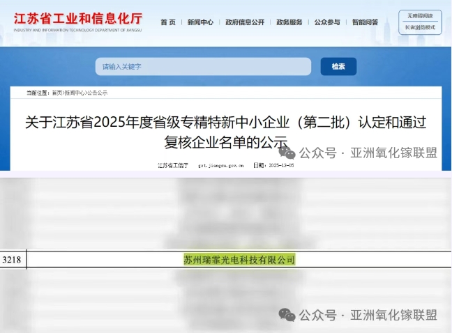
In December 2025, Suzhou Raphael Optech was officially recognized as a “Specialized, Refined, Distinctive, and Innovative” enterprise by Jiangsu Province. The company continues to support the research and production of Gallium Oxide and other ultra-wide bandgap semiconductor materials through its optical 3D inspection technologies. Its independently developed equipment, including wafer warp stress meters and geometric morphology measurement instruments, provides precise support for analyzing wafer microstructure, thin-film stress, and defect identification, ensuring material performance and device yield. With strong technical expertise, Suzhou Raphael Optech is providing core inspection capabilities that support the industrialization of Gallium Oxide and the development of high-end semiconductors in China.
GaFuture Semiconductor Technology: Founded by the Xidian University Team, Independently Develops HVPE Equipment and Heteroepitaxy Technology, Reducing Epitaxial Wafer Costs by Over 10×
In July 2025, GaFuture Semiconductor Technology (Jinjiang) Co., Ltd. was officially established in Jinjiang, Fujian Province, with a focus on the research and industrialization of Gallium Oxide (β-Ga₂O₃) heteroepitaxial materials.
In November 2025, GaFuture Semiconductor Technology achieved a strategic breakthrough in Gallium Oxide epitaxial materials. Through independently developed HVPE equipment and heteroepitaxy technology, the company significantly reduced production costs, improved material performance, and solved long-standing technical challenges limiting industrialization. Focusing on high-value application scenarios such as new energy vehicles, high-voltage industrial power supplies, and solar-blind ultraviolet optoelectronic detection, the company implements a phased market expansion strategy, gradually extending from research services to industrial applications. These initiatives not only strengthen GaFuture Semiconductor Technology’s technical foundation in fourth-generation semiconductor materials but also establish its core competitiveness and first-mover advantage for scaling Gallium Oxide from the laboratory to large-scale industrialization.
Shanghai: Laying Out the Gallium Oxide Industry and Building a Frontier for Ultra-Wide Bandgap Semiconductor Innovation
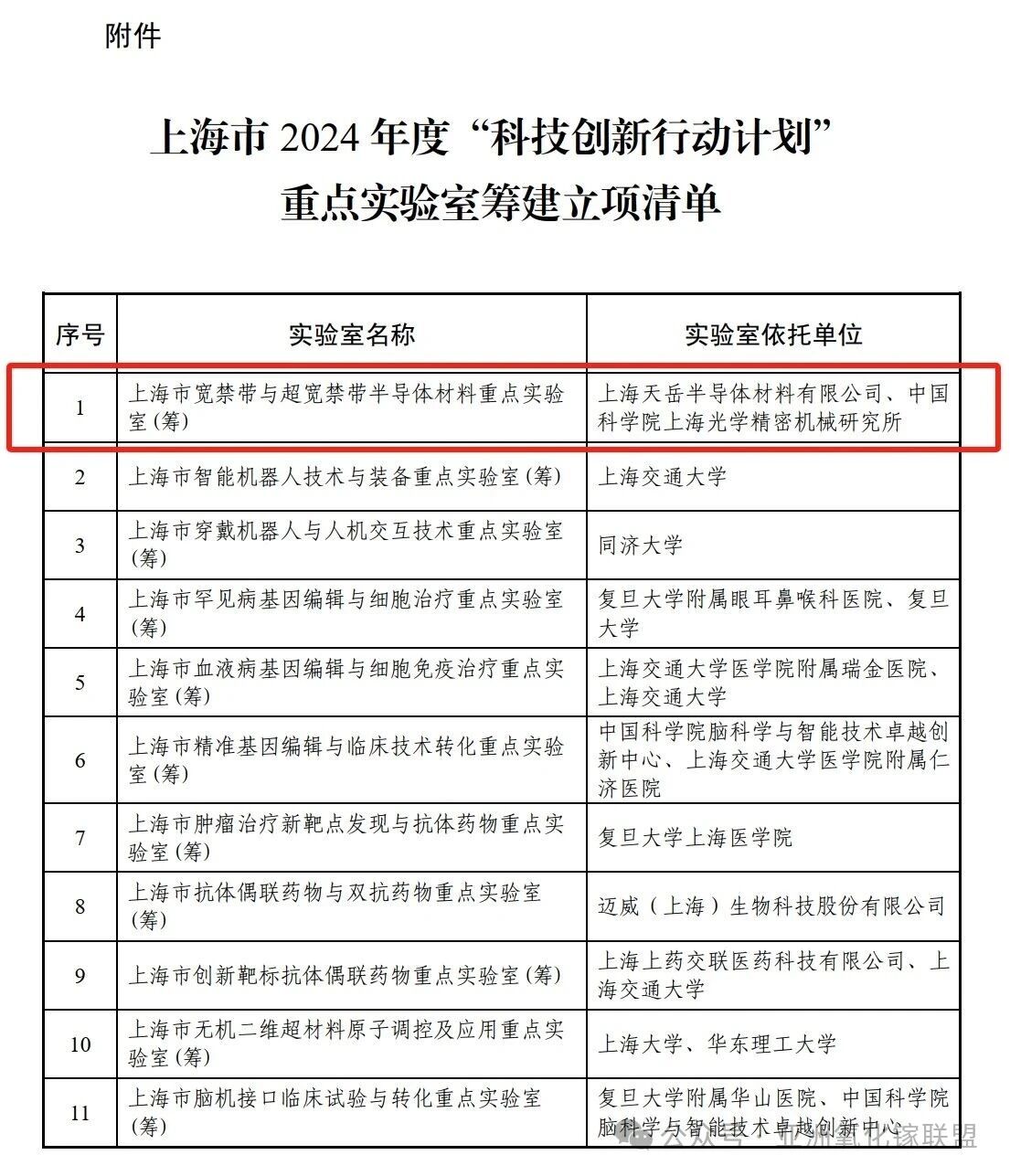
In January 2025, Shanghai launched the construction plan for the Key Laboratory of Wide- and Ultra-Wide Bandgap Semiconductor Materials, focusing on the fundamental theories and industrialization technologies of strategic ultra-wide bandgap materials such as Gallium Oxide. The laboratory leverages the collaboration between Shanghai Tianyue and the Shanghai Institute of Optics and Fine Mechanics, centering on the preparation of large-size, low-cost, and low-dislocation-density materials. It aims to deeply integrate scientific research outcomes with industrial applications, establishing a globally leading semiconductor innovation hub, fostering new productivity, and supporting the high-quality development and international competitiveness of Shanghai’s wide-bandgap semiconductor industry.
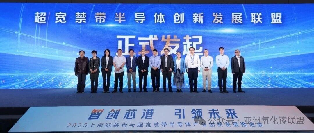
In May 2025, the Shanghai Wide- and Ultra-Wide Bandgap Semiconductor Industry Innovation and Development Conference was held in the Lingang New Area, marking the official launch of Shanghai’s systematic layout in the ultra-wide bandgap semiconductor field. During the conference, the key laboratory was inaugurated, industrial clusters were initiated, supporting policies and industry funds were released, and an innovation and development alliance was established. This initiative gathers research, industrial, and financial resources to lay a solid foundation for technological breakthroughs and industrial applications of Gallium Oxide and other ultra-wide bandgap materials, advancing Shanghai toward a globally leading semiconductor innovation hub.
Conclusion
In 2025, China’s Gallium Oxide industry demonstrated breakthroughs across the entire value chain and rapid progress. On the materials side, single-crystal sizes continued to scale from 2-inch and 4-inch to 6-inch and 8-inch, and epitaxial wafer performance steadily improved, providing reliable support for high-voltage power devices and optoelectronic applications. On the device side, achievements such as high-mobility epitaxial wafers and vertical-type power Schottky diodes underwent engineering verification, driving the translation from laboratory research to industrial implementation. In terms of the industrial chain, laboratory advances, capacity expansions, and strategic collaborations accelerated the transition of Gallium Oxide from research to engineering-scale and mass applications. The coordinated push of policies, capital, and scientific research has enabled Gallium Oxide to move from a potential material to formal application, further consolidating China’s technological strength and industrial competitiveness in the ultra-wide bandgap semiconductor field. The future development prospects of Gallium Oxide are highly promising.
