Paper Sharing
【Member Papers】Universal Role of Dopant-VGa Complexes Induced Carrier Suppression in Si/Ge/Sn/Zr-doped β-Ga₂O₃
日期:2026-02-02阅读:346
Researchers from the Wuhan University have published a dissertation titled " Universal Role of Dopant-VGa Complexes Induced Carrier Suppression in Si/Ge/Sn/Zr-doped β-Ga2O3 " in Applied Physics Lettes.
Background
β-Ga₂O₃, with its ultra-wide bandgap (~4.9 eV) and high breakdown field, is regarded as a key material for high-power electronic devices. In this context, achieving efficient and stable n-type doping is fundamental for advancing the practical application of β-Ga₂O₃ in electronic devices. Dopants such as Si, Sn, Ge, and Zr can introduce shallow donor defects in β-Ga₂O₃, but their n-type doping efficiency is limited by the “self-compensation” effect, which makes it challenging to further increase the carrier concentration. Although previous studies have identified VGa (gallium vacancies) as a critical compensating defect, the systematic atomic-scale compensation mechanisms associated with these four major n-type dopants—including their formation origins and energy level positions—have not yet been fully understood.
Abstract
The development of high-performance β-Ga2O3 electronics is critically hindered by the fundamental limitation of self-compensation in n-type doping, which severely suppresses free carrier concentrations. To explore the microscopic mechanism of this effect, we systematically investigate the four n-type dopants (Si, Sn, Ge, and Zr) in β-Ga2O3, combining first-principles calculations and experimental investigations. The calculation results show that the lower formation energies of SiGaVGa and SnGaVGa complexes compared to GeGaVGa and ZrGaVGa complexes lead to their higher concentrations and consequently stronger compensation in Si and Sn doping β-Ga2O3 under O-rich conditions. Oxygen annealing induces a severe compensation effect, as consistently validated by Hall effect and non-contact eddy current measurements. Beyond this universal mechanism, we further identify that the carrier compensation predominantly occurs near the surface, manifesting as a dramatic drop in near-surface carrier concentration and a sharp increase in contact resistivity in Sn-doped β-Ga2O3. Furthermore, photoluminescence spectra exhibit distinct green emission (∼2.5 eV), confirming the formation of the predicted deep-level defects SnGaVGa. This work reveals the microscopic compensation mechanism, providing vital theoretical and experimental insights for optimizing n-type β-Ga2O3 conductivity.
Conclusion
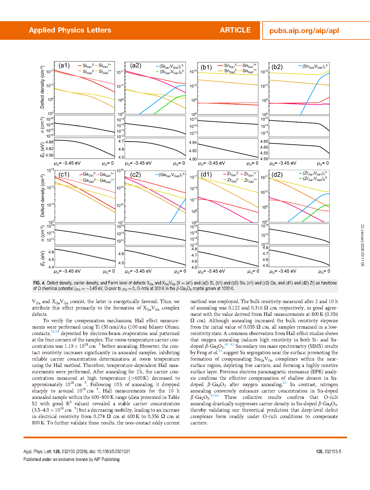
This study combines theoretical calculations with experimental validation to investigate the self-compensation effect in n-type β-Ga₂O₃. Density functional theory (DFT) calculations indicate that stable XGaVGa complexes (X = Si, Ge, Sn, Zr) act as the primary defect centers responsible for carrier compensation, severely limiting the n-type conductivity of the material. Among them, the formation of SiGaVGa and SnGaVGa complexes is particularly pronounced. This theoretical prediction was experimentally confirmed in Sn-doped β-Ga₂O₃: after annealing in an oxygen atmosphere, the carrier concentration decreased from ~10¹⁸ cm⁻³ (room-temperature Hall measurement) to 10¹⁶ cm⁻³ (high-temperature Hall measurement above 600 K). Photoluminescence (PL) spectra exhibited characteristic emission peaks around 2.5 eV associated with deep-level defects, corresponding well to the SnGaVGa complexes formed during annealing, further supporting the proposed defect configuration. This work elucidates the atomic-scale physical origin of self-compensation across different doping systems, providing key theoretical and experimental guidance for optimizing β-Ga₂O₃ conductivity via annealing atmosphere control and defect suppression, and holds significant implications for advancing its application in high-performance power electronic devices.
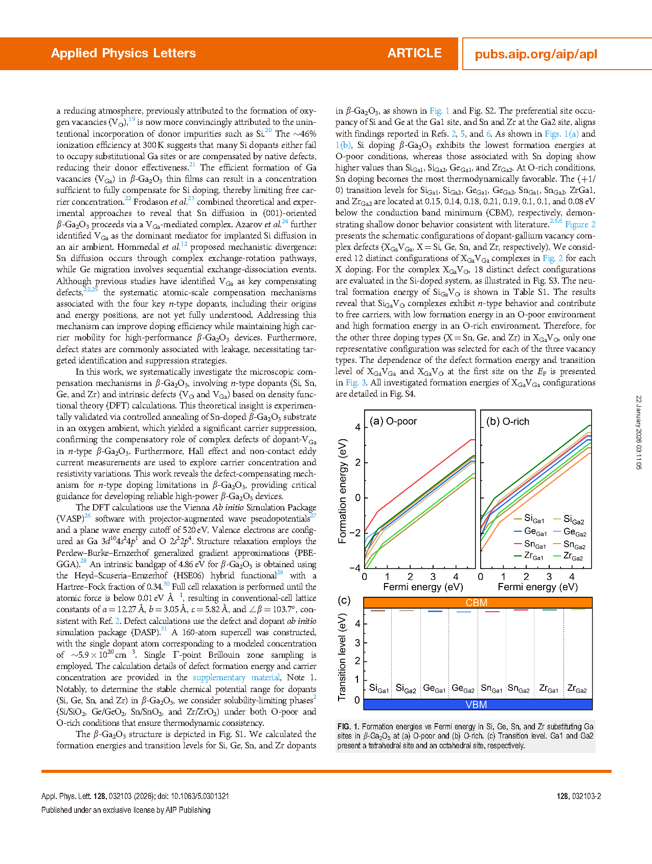
FIG. 1. Formation energies vs Fermi energy in Si, Ge, Sn, and Zr substituting Ga sites in β-Ga2O3 at (a) O-poor and (b) O-rich. (c) Transition level. Ga1 and Ga2 present a tetrahedral site and an octahedral site, respectively.
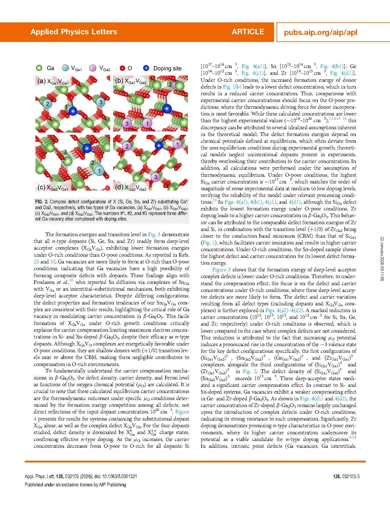
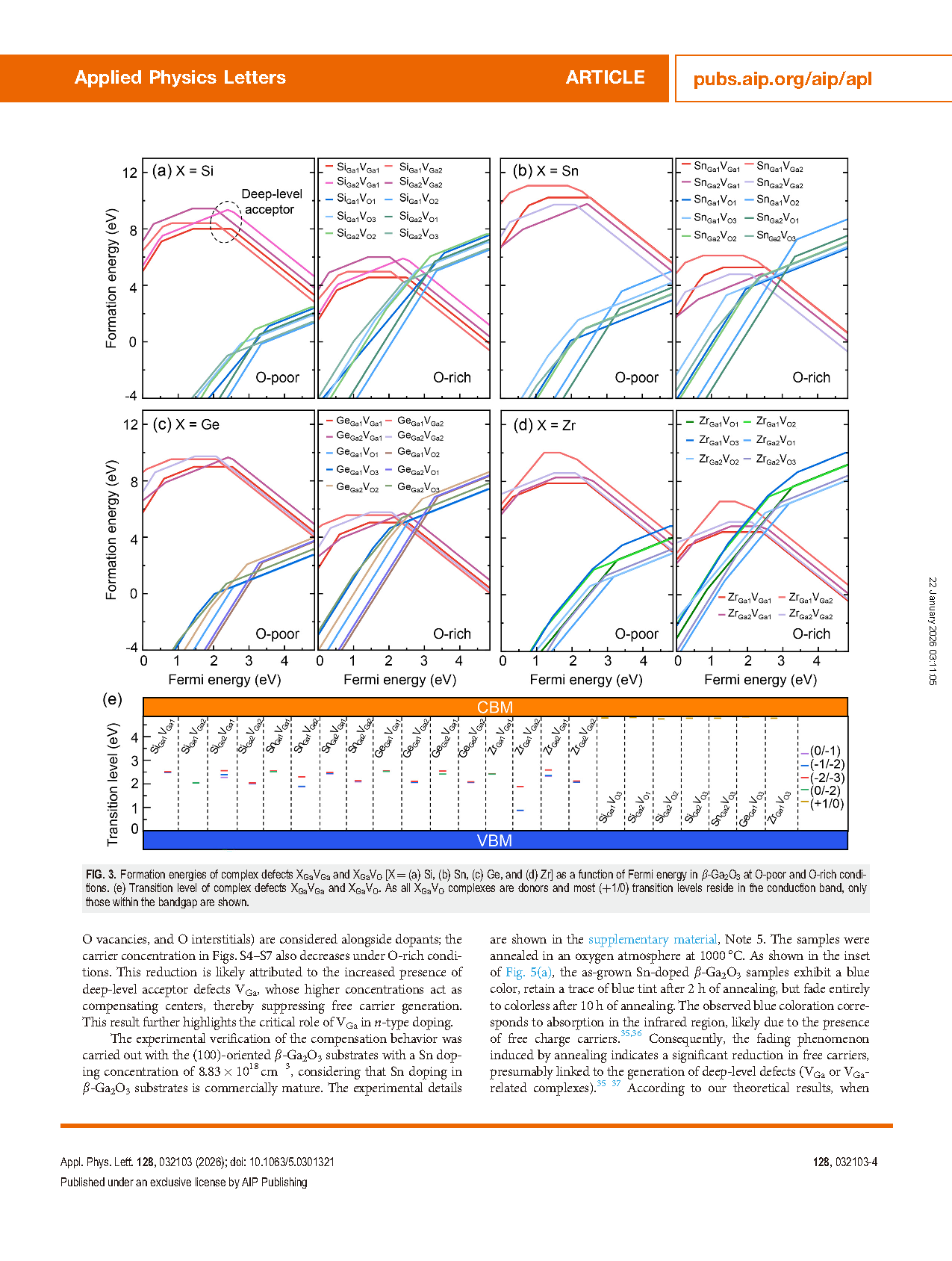
FIG. 2. Formation energies of complex defects XGaVGa and XGaVO [X ¼ (a) Si, (b) Sn, (c) Ge, and (d) Zr] as a function of Fermi energy in β-Ga2O3 at O-poor and O-rich conditions. (e) Transition level of complex defects XGaVGa and XGaVO. As all XGaVO complexes are donors and most (þ1/0) transition levels reside in the conduction band, only those within the bandgap are shown.
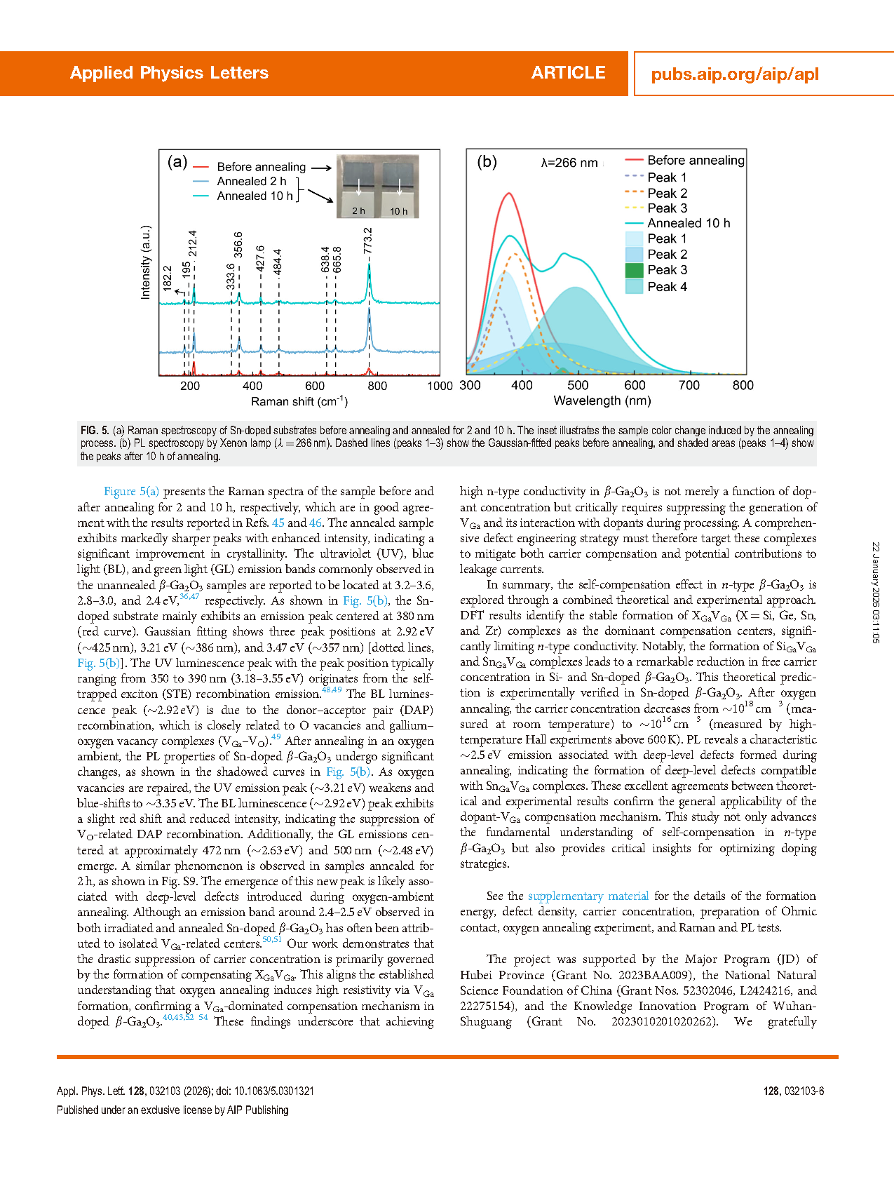
FIG. 3. (a) Raman spectroscopy of Sn-doped substrates before annealing and annealed for 2 and 10 h. The inset illustrates the sample color change induced by the annealing process. (b) PL spectroscopy by Xenon lamp (k ¼ 266 nm). Dashed lines (peaks 1–3) show the Gaussian-fitted peaks before annealing, and shaded areas (peaks 1–4) show the peaks after 10 h of annealing.
DOI:
10.1063/5.0301321