Paper Sharing
【Member Papers】Review of Mist-CVD Technology for Ga₂O₃ Power and Optoelectronic Devices
日期:2026-02-02阅读:377
Researchers from the Fudan University have published a dissertation titled "Review of Mist-CVD Technology for Ga₂O₃ Power and Optoelectronic Devices" in 2025 22nd China International Forum on Solid State Lighting & 2025 11th International Forum on Wide Bandgap Semiconductors (SSLCHINA: IFWS).
Project Support
This work is supported by the National Key R&D Program of China (2023YFB4606300), the National Natural Science Foundation of China (62474049), the Science and Technology Innovation Plan of Shanghai Science and Technology Commission (No.21DZ110080,23ZR1405300) and the Joint Research Plan of sci-tech innovation community in Yangtze River Delta (No. 2023CSJG0600).
Background
Driven by the rapid growth of emerging industries such as new energy vehicles, 5G communications, photovoltaics, and energy storage, as well as intensifying global technological competition, the demand for high-performance power electronic materials is increasing. While Silicon Carbide (SiC) and Gallium Nitride (GaN) are widely used, they may not represent the ultimate frontier in power electronics. Recently, Gallium Oxide (Ga₂O₃) has attracted significant attention from governments and industries due to its wide bandgap, high breakdown electric field, and availability of large-area native substrates, making it a strategic emerging material with substantial growth potential. The successful development of Ga₂O₃-based devices critically depends on epitaxial growth techniques that can produce high-quality thin films at low cost and with scalability. Conventional methods such as molecular beam epitaxy (MBE), metal-organic chemical vapor deposition (MOCVD), and hydride vapor phase epitaxy (HVPE) can yield high-quality films but are limited by high equipment costs, complex operation, and scalability issues. In this context, mist chemical vapor deposition (Mist-CVD) has emerged as a promising alternative, offering non-vacuum operation, simple process, and precise control over doping concentration and film thickness. Mist-CVD enables the growth of high-quality Ga₂O₃ layers on large-area substrates at reduced cost and has been successfully applied to Schottky barrier diodes (SBDs), MESFETs, MOSFETs, and solar-blind ultraviolet photodetectors, demonstrating its potential for both academic research and industrial-scale applications.
Abstract
Gallium oxide (Ga2O3), an ultrawide bandgap (UWBG) semiconductor, has been widely recognized as a promising material for next-generation power and optoelectronic devices due to its wide bandgap (4.6−4.9eV), high breakdown electric field, and availability of large-area substrates. However, the practical commercialization of Ga2O3 devices requires epitaxial technologies capable of delivering high-quality layers at low cost and high efficiency. Mist chemical vapor deposition (Mist-CVD) has emerged as a promising alternative to address these limitations. Distinguished by its vacuum-free operation, simple process, low cost, and compatibility with large-area growth, Mist-CVD also provides precise control over doping concentration, film thickness, and crystalline quality. These advantages make it an attractive route for advancing both research and commercialization of Ga2O3-based devices. In power electronics, Ga2O3 grown by Mist-CVD has been successfully applied to Schottky barrier diodes (SBDs), Metal-Semiconductor Field Effect Transistors (MESFETs) and Metal Oxide Semiconductor Field Effect Transistors (MOSFETs), demonstrating competitive voltages and leakage currents. In optoelectronics, the intrinsic absorption edge of Ga2O3 at around 250 nm naturally enables solar-blind ultraviolet detection without the need for bandgap engineering. As a result, Mist-CVD-grown Ga2O3 layers are highly suitable for solar-blind photodetectors and deep-UV sensors, exhibiting high responsivity, low dark current, and excellent spectral selectivity. This review summarizes recent advances in the application of Mist-CVD for Ga2O3-based power and optoelectronic devices and discusses current challenges and future perspectives toward its industrial deployment.
Conclusion
Based on the comprehensive review, it is evident that Mist-CVD has established itself as a highly competitive and versatile epitaxial technique for fabricating both power and optoelectronic devices based on Ga2O3. Its distinctive advantages, including vacuum-free operation, low cost, simplicity, and compatibility with large-area substrates, address critical limitations of conventional methods like MBE and MOCVD. For power electronics, Mist-CVD-grown Ga2O3 has enabled high-performance SBDs, MESFETs, and MOSFETs, demonstrating remarkable breakdown voltages, low specific on-resistances, and excellent power figures of merit. In the realm of optoelectronics, the technique facilitates the deposition of high-quality layers for solar-blind photodetectors, achieving outstanding responsivities, ultralow dark currents, and high detectivity. The findings indicate that Mist-CVD not only enables precise regulation of film composition and thickness but also contributes to enhanced electrical and optical characteristics of devices. Overall, this work provides a comprehensive understanding of Mist-CVD as a promising and scalable technique for next-generation semiconductor device fabrication.
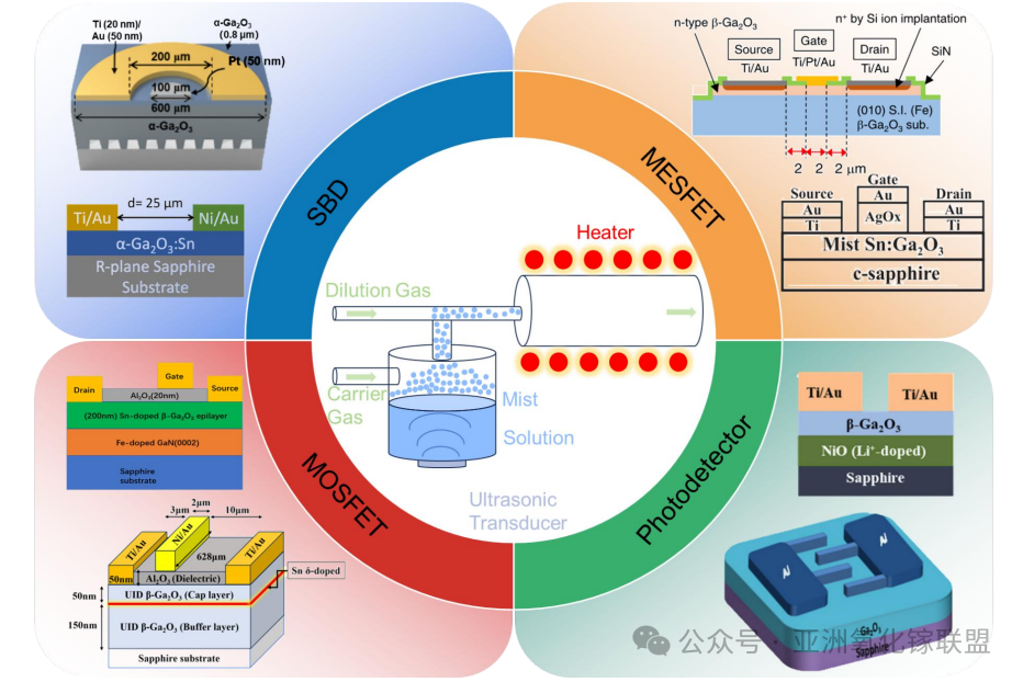
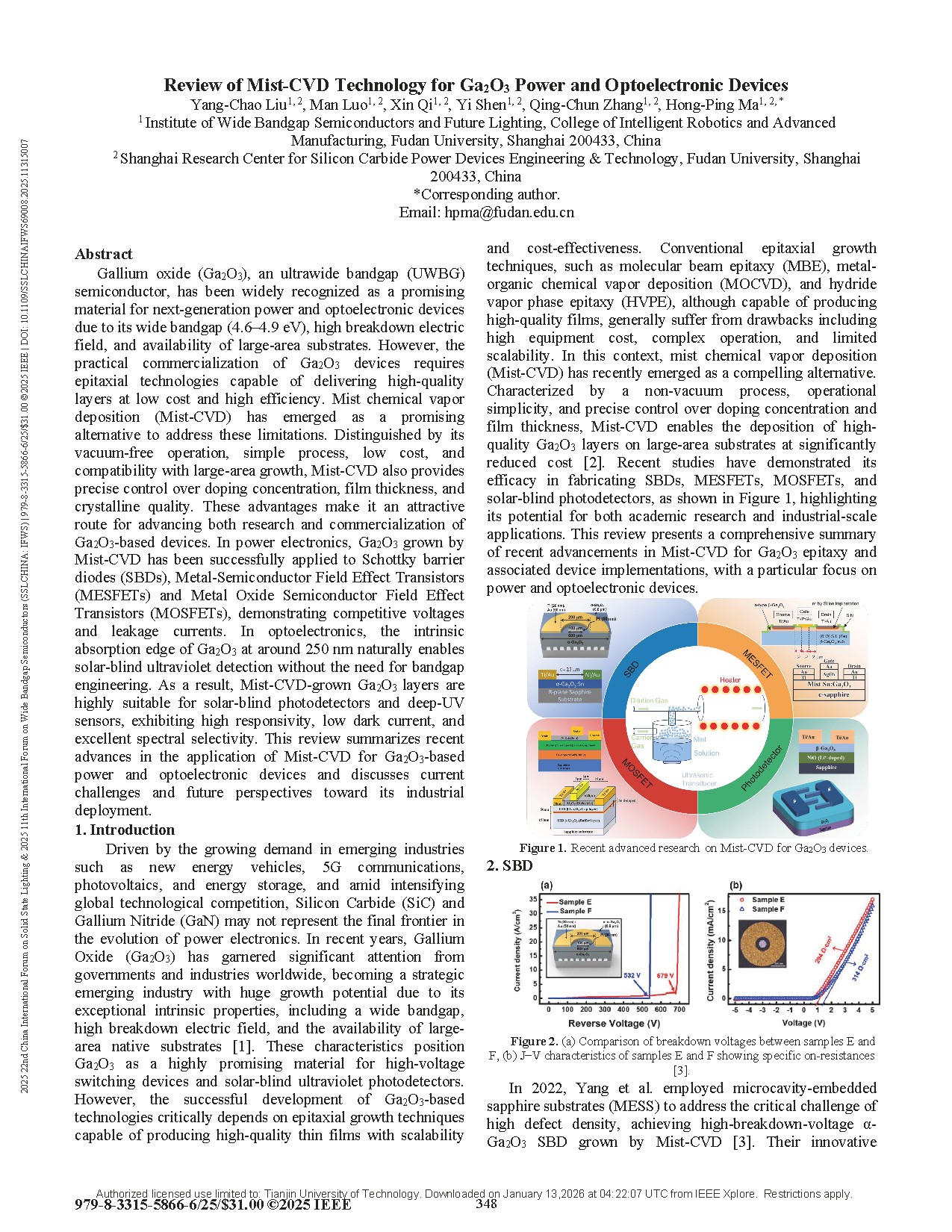
Figure 1. Recent advanced research on Mist-CVD for Ga2O3 devices.
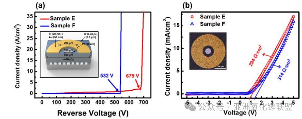
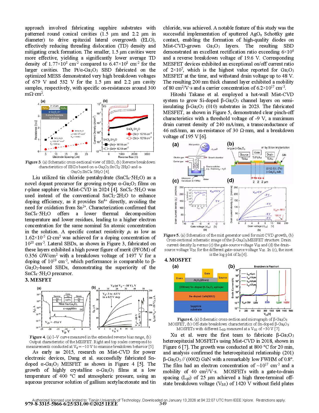
Figure 2. (a) Comparison of breakdown voltages between samples EandF, (b) J−V characteristics of samples E and F showing specific on-resistances.
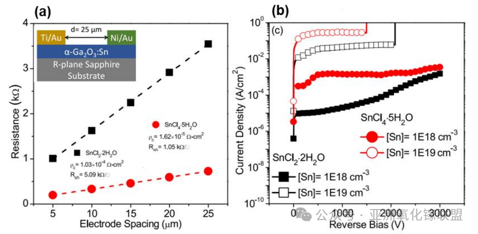
Figure 3. (a) Schematic cross-sectional view of SBD, (b) Reverse breakdown characteristics of SBDs based on α-Ga2O3:SnCl2·2H2O and α-Ga2O3:SnCl4·5H2O.
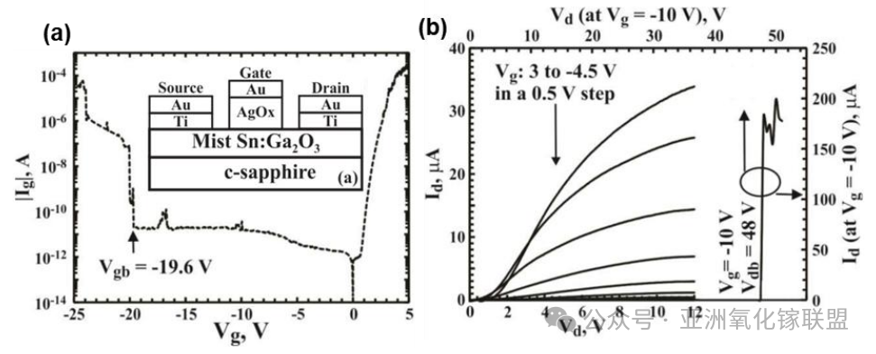
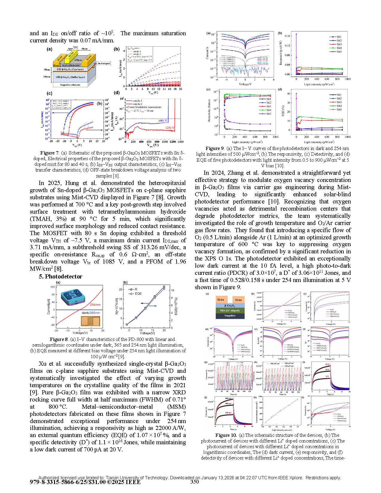
Figure 4. (a) I–V curve measured in the extended reverse bias range, (b) Output characteristic of the MESFET. Right and top scales correspond to measurements conducted at Vg = −10 V to examine breakdown behavior.
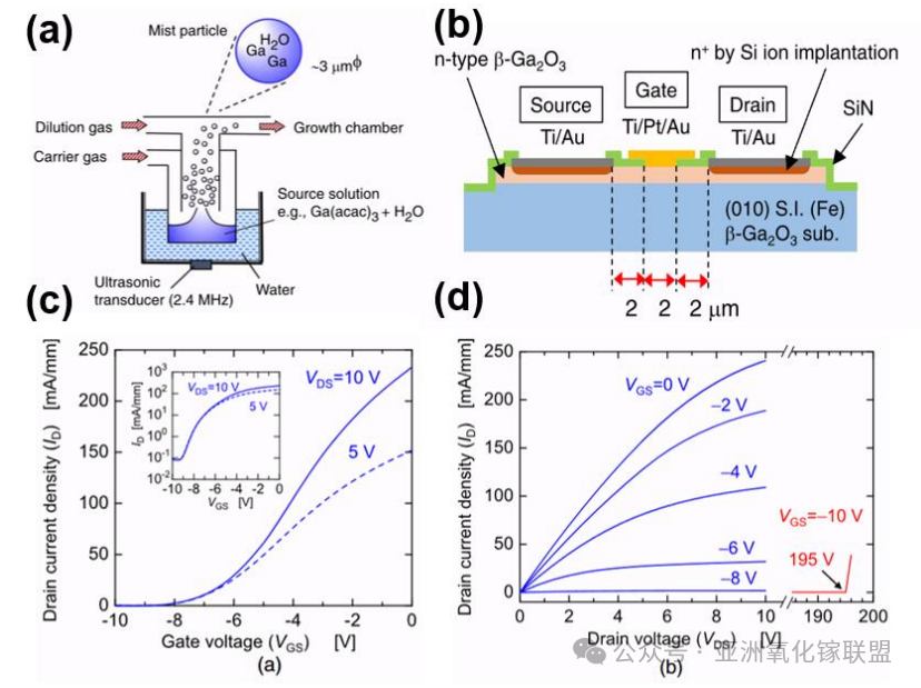
Figure 5. (a) Schematics of the mist generator used for mist CVD growth, (b)Cross-sectional schematic image of the β-Ga2O3 MESFET structure. Drain current density ID versus (c) the gate-source voltage VGS and (d) the drain- source voltage VDS for the different gate–source voltage VGS. In (c), the inset is the log plot of ID.
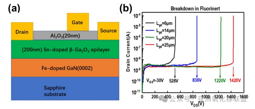
Figure 6. (a) Schematic cross-section and micrograph of β-Ga2O3 MOSFET, (b) Off-state breakdown characteristics of Sn-doped β-Ga2O3 MOSFETs with different LGD measured at a VGS of −30 V.
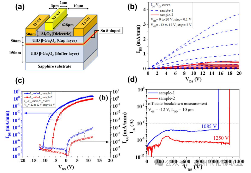
Figure 7. (a) Schematic of the proposed β-Ga2O3 MOSFETs with Sn δ- doped, Electrical properties of the proposed β-Ga2O3 MOSFETs with Sn δ- doped mist for 80 and 40 s, (b) IDS–VDS output characteristics, (c) IDS–VGS transfer characteristics, (d) OFF-state breakdown voltage analysis of two samples.
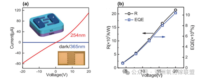
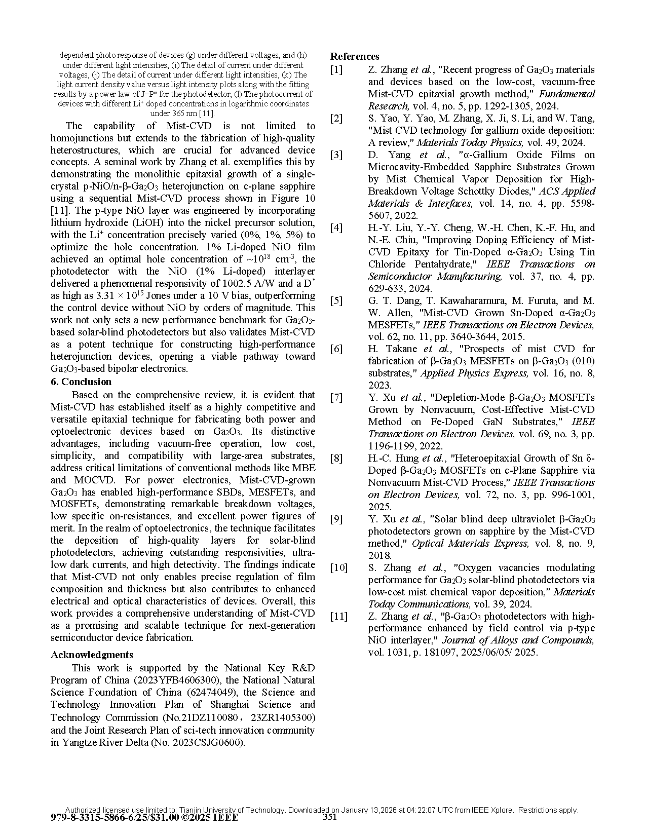
Figure 8. (a) I–V characteristics of the PD-800 with linear and semilogarithmic coordinates under dark, 365 and 254 nm light illumination, (b) EQE measured at different bias voltage under 254 nm light illumination of 100 µW cm−2.
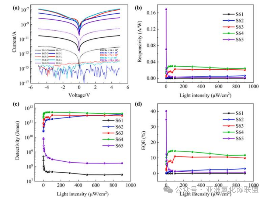
Figure 9. (a) The I−V curves of the photodetectors in dark and 254nm light intensities of 500 μWcm−2, (b) The responsivity, (c) Detectivity, and(d)EQE of five photodetectors with light intensity from 0.5 to 900 μWcm−2 at 5V bias.
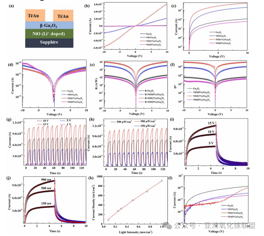
Figure 10. (a) The schematic structure of the devices, (b) The photocurrent of devices with different Li+ doped concentrations, (c) The photocurrent of devices with different Li+ doped concentrations in logarithmic coordinates, The (d) dark current, (e) responsivity, and(f) detectivity of devices with different Li+ doped concentrations, The time dependent photo response of devices (g) under different voltages, and (h) under different light intensities, (i) The detail of current under different voltages, (j) The detail of current under different light intensities, (k) The light current density value versus light intensity plots along with the fitting results by a power law of J−Pα for the photodetector, (l) The photocurrent of devices with different Li+ doped concentrations in logarithmic coordinates under 365 nm.
DOI:
doi.org/10.1109/SSLCHINAIFWS69008.2025.11315007