Paper Sharing
【Member Papers】Simple (YGa)₂O₃/F-SnO₂ Heterojunction-Based Solar-Blind Ultraviolet Photodetector Operable in Two Modes With Superb Performance
日期:2026-02-02阅读:354
Researchers from the Wuhan Textile University have published a dissertation titled "Simple (YGa)2O3/F-SnO2 Heterojunction-Based Solar-Blind Ultraviolet Photodetector Operable in Two Modes With Superb Performance" in ENERGY & ENVIRONMENTAL MATERIALS.
Project Support
This work was supported bythe National Natural Science Foundation of China (Grant Nos. 62274057,11975093, and 52202132), the Sino-German Center for Research Promotion(Grant No. M-0764), and the Program for Science and Technology InnovationTeam in Colleges of Hubei Province (Grant No. T201901).
Background
Solar-blind ultraviolet (SBUV) photodetectors, with extremely low background noise and high sensitivity, hold great potential for applications in smart power-grid monitoring, flame detection, medical imaging, missile warning and tracking, space communications, and other fields. Traditional SBUV photodetectors based on GaN, SiC, or Si suffer from bandgap limitations or require expensive visible-light filters. In recent years, ultrawide-bandgap semiconductors (Eg > 4.4 eV), such as Ga₂O₃, AlGaN, diamond, and MgZnO, have attracted attention due to their wide bandgaps, high stability, and tunability. Among them, Ga₂O₃ is particularly promising, as its bandgap can be further engineered via alloying, making it suitable for solar-blind detection. However, common oxygen vacancies in Ga₂O₃ films lead to high dark current and long response times, limiting device performance. Alloying with suitable rare-earth elements (e.g., Y³⁺) to form (YGa)₂O₃ (YGO) can effectively suppress oxygen vacancies, reduce dark current, accelerate response, and simultaneously widen the bandgap, improving sensitivity to weak SBUV signals. Self-driven photodetectors can operate without an external power supply and often employ heterojunctions or Schottky junctions for efficient separation and collection of photogenerated carriers. Therefore, introducing YGO alloys to fabricate vertical-structured YGO/FTO heterojunction photodetectors enables high-sensitivity detection of extremely weak solar-blind signals under both self-driven and biased modes, while offering fast response and excellent performance.
Abstract
Gallium oxide (Ga2O3), with its wide direct bandgap (~4.9 eV) and high stability, holds great potential for applications in solar-blind ultraviolet (SBUV) photodetectors. In this work, simple vertical-structured SBUV photodetectors based on (YGa)2O3/F-SnO2 (YGO/FTO) heterojunctions were designed and fabricated for the first time. Owing to the wider bandgap of Y2O3 (~5.9 eV) compared to Ga2O3 and the stronger Y–O bonding relative to Ga–O, the YGO alloy films exhibit an expanded bandgap (~5.2 eV) with fewer oxygen vacancies than pure Ga2O3. This results in SBUV photodetectors with an extremely low dark current and fast photoresponse. Moreover, the YGO/FTO-based photodetectors demonstrate excellent performance in both biased and self-driven modes. At 0 V bias, the photodetector with a YGO layer thickness of 246 nm exhibits an exceptionally low dark current of 0.145 pA, a short photoresponse time of 15 ms, high responsivity of 12.2 mA W−1, and a detectivity of 2.84 × 10¹² Jones. At a bias of −10 V, the device with a 425 nm-thick YGO layer achieves a high photocurrent/dark current (Iphoto/Idark) ratio of 106, UV/visible rejection ratio of 105, and remarkably high responsivity of 12.3 A W−1 with a detectivity of 1.08 × 10¹⁵ Jones. These results highlight the great promise of YGO alloys in developing simple vertical-structured YGO/FTO high-performance photodetectors for ultraweak SBUV detection.
Conclusion
In this study, we report a simple SBUV photodetector fabricated by directly depositing a YGO film on a widely available FTO substrate, showing excellent performance under both zero and negative bias conditions. By incorporating yttrium into Ga2O3, the photodetector achieves an ultralow dark current and overcomes the issue of high background current common in vertical-structured photodetectors. Under 0 V bias, the d246 nm-YGO /FTO-based photodetector exhibits a dark current of only 0.145 pA, a fast photoresponse time of 15 ms, a high responsivity of 12.2 mA W−1, and a detectivity of 2.84 × 10¹² Jones. Under −10 V bias, the d425 nm-YGO/FTO-based photodetector exhibits a high Iphoto/Idark ratio of 106, a UV/visible rejection ratio of 105, an excellent responsivity of 12.3 A W−1, and a detectivity of 1.08 × 10¹⁵ Jones. These results indicate that the simple vertically structured Au/YGO/FTO SBUV photodetector has strong potential for future optoelectronic applications.
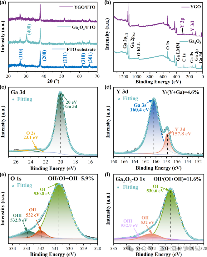
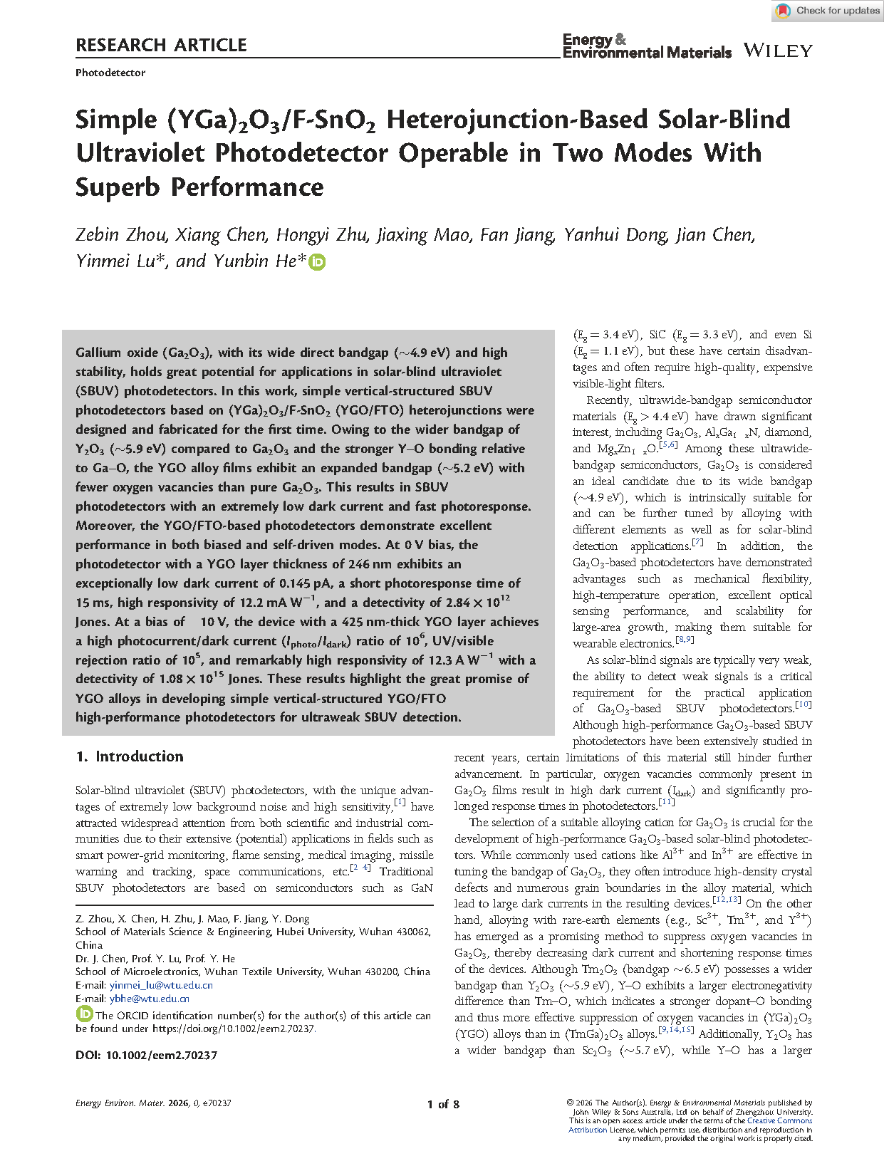
Figure 1 a) XRD patterns of a representative YGO film, pure Ga2O3 film, and the FTO substrate. b) XPS survey spectra of pure Ga2O3 and YGO films. c) Ga 3d and d) Y 3d core-level spectra of the YGO film, and O 1s core-level spectra of e) the YGO and f) pure Ga2O3 films calibrated with respect to the C 1s peak at 284.8 eV.

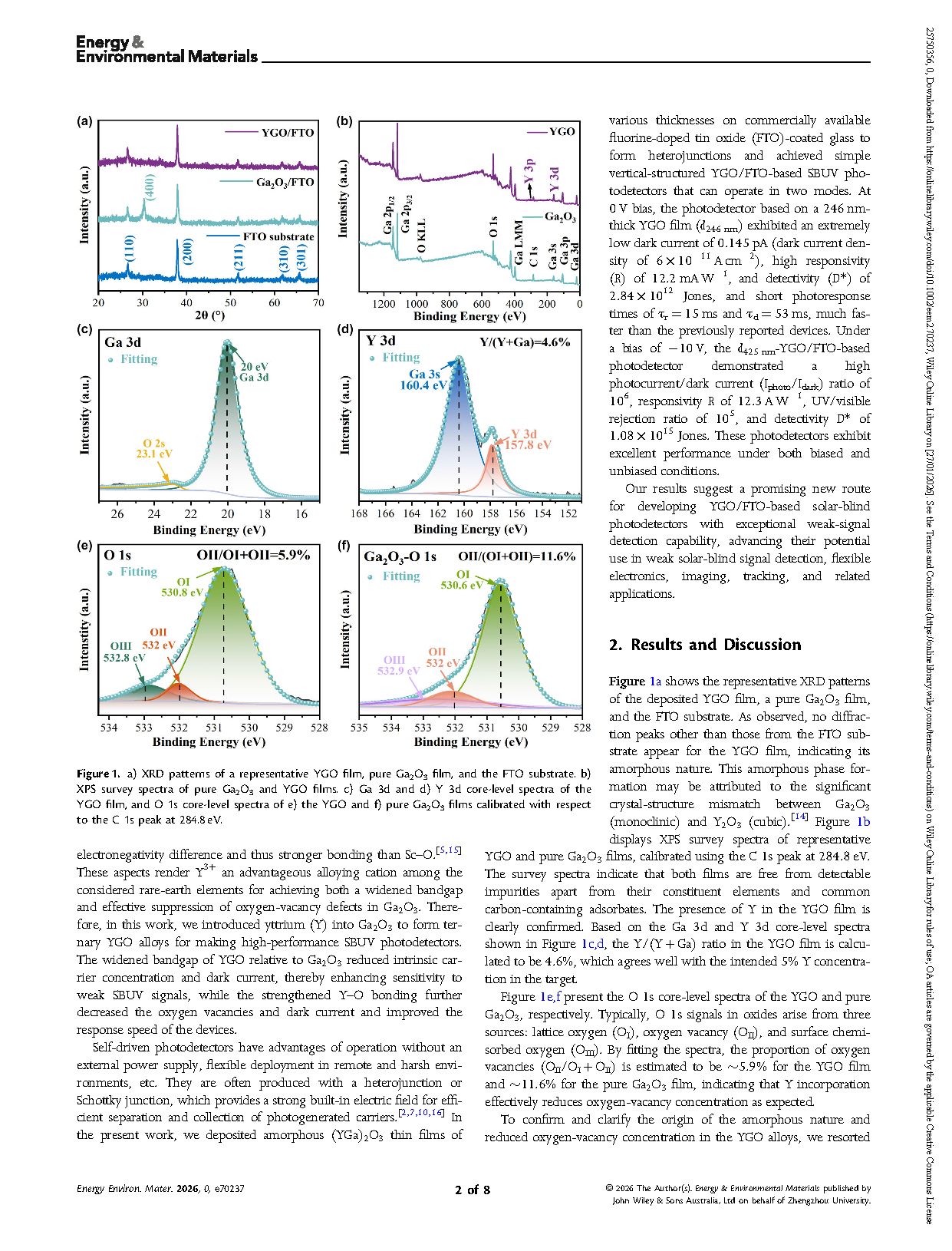
Figure 2 a) Cross-sectional FE-SEM images and EDS element-mapping, and b) 2D and 3D AFM images of (Y0.05Ga0.95)2O3 films with thicknesses of 246 and 425 nm, respectively. c) Transmittance spectra and d) plots of (αhν)2 versus hν of (Y0.05Ga0.95)2O3 films with the same thicknesses grown on c-plane sapphire. The inset in (c) shows the transmittance spectrum of the FTO substrate.
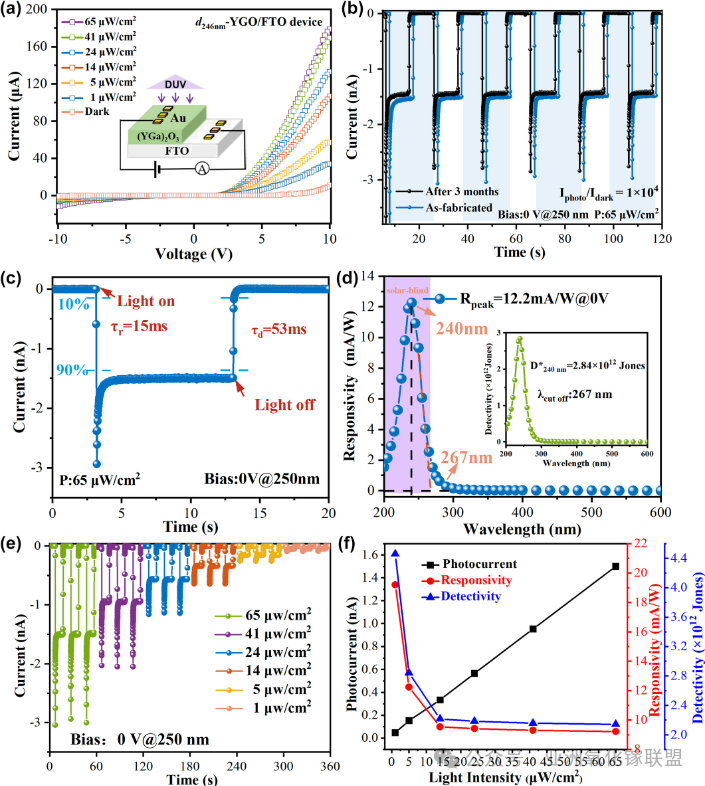
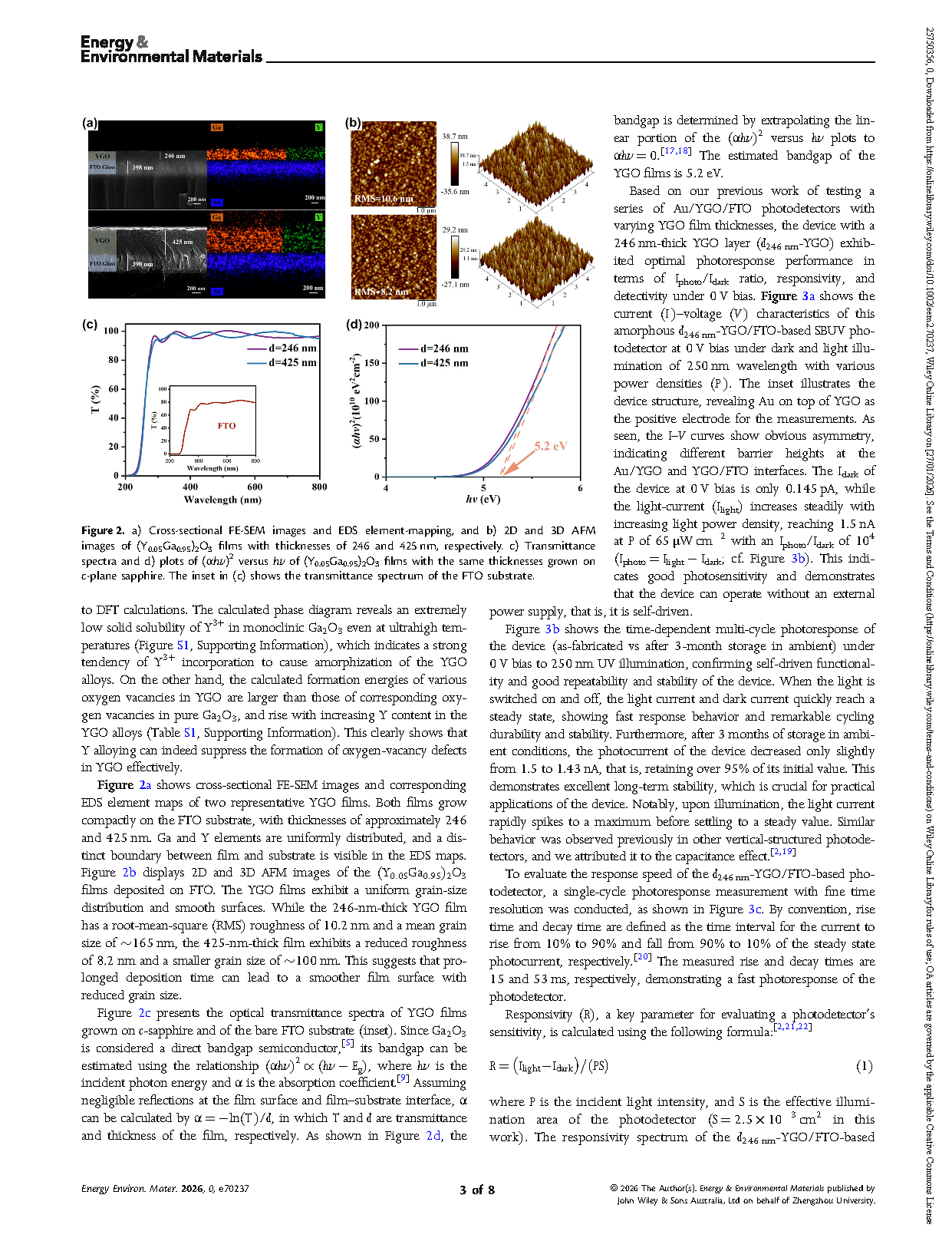
Figure 3 Photoresponse characteristics of the d246 nm-YGO/FTO-based photodetector in self-driven mode. a) Current–voltage curves of the device under dark and illumination with 250 nm-light of different light intensities. b) The multi-cycle photoresponse of the device in as-fabricated state and after 3-month storage in ambient, and c) single-cycle photoresponse showing the rise/decay edges of the device under 0 V bias to 250 nm-light illumination with power density of 65 μW cm−2. d) Spectral responsivity and detectivity (inset) of the device under 0 V bias. e) Time-dependent photoresponse of the device under 0 V bias to 250 nm-light illumination with various light intensities. f) Variation of the photocurrent, R, and D* of the photodetector with light intensities.
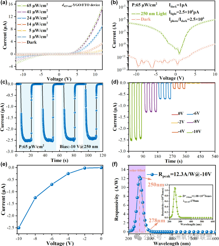
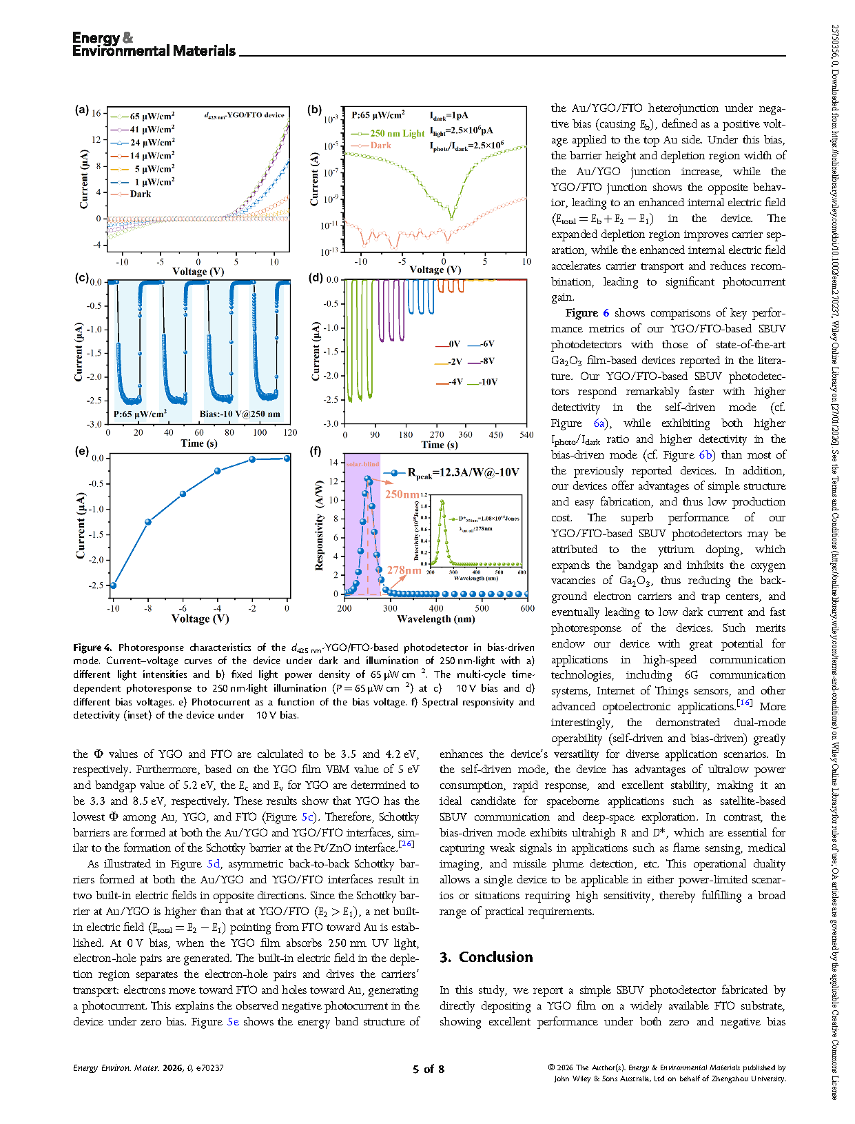
Figure 4 Photoresponse characteristics of the d425 nm-YGO/FTO-based photodetector in bias-driven mode. Current–voltage curves of the device under dark and illumination of 250 nm-light with a) different light intensities and b) fixed light power density of 65 μW cm−2. The multi-cycle time-dependent photoresponse to 250 nm-light illumination (P = 65 μW cm−2) at c) −10 V bias and d) different bias voltages. e) Photocurrent as a function of the bias voltage. f) Spectral responsivity and detectivity (inset) of the device under −10 V bias.
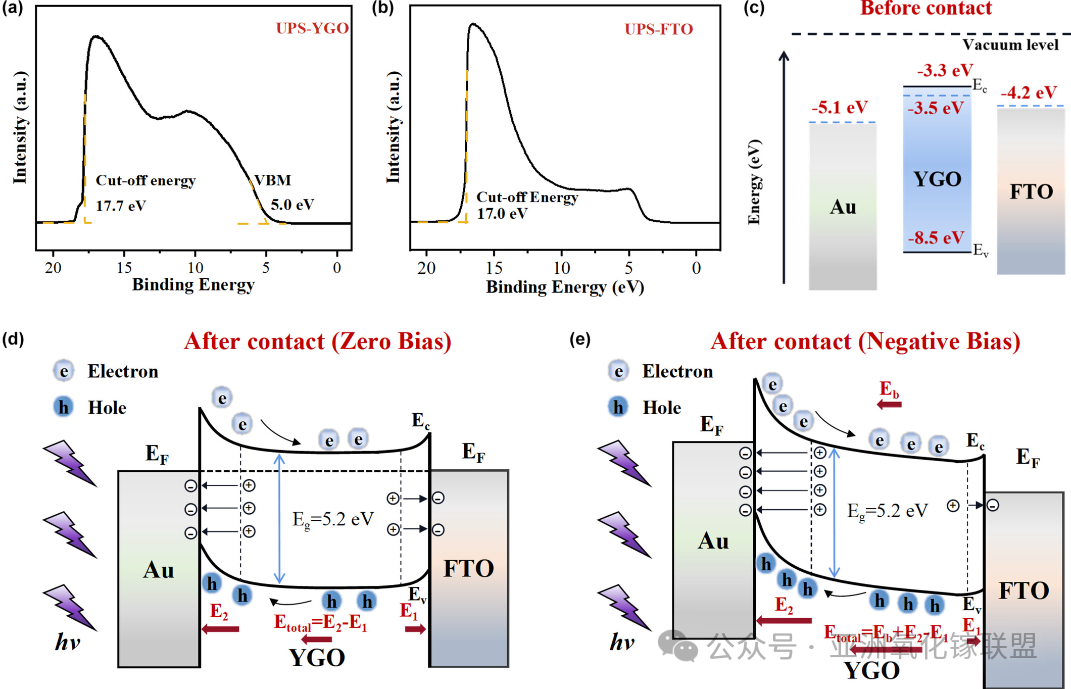
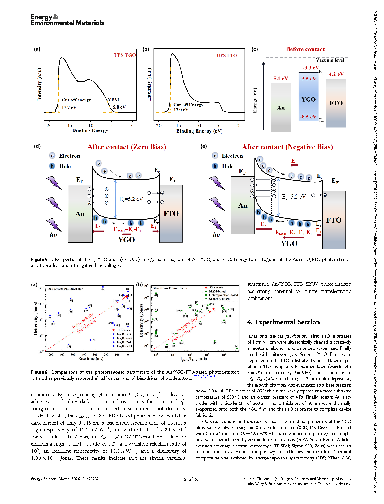
Figure 5 UPS spectra of the a) YGO and b) FTO. c) Energy band diagram of Au, YGO, and FTO. Energy band diagram of the Au/YGO/FTO photodetector at d) zero bias and e) negative bias voltages.
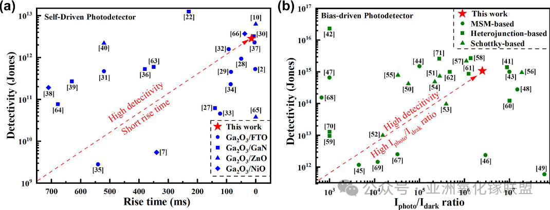
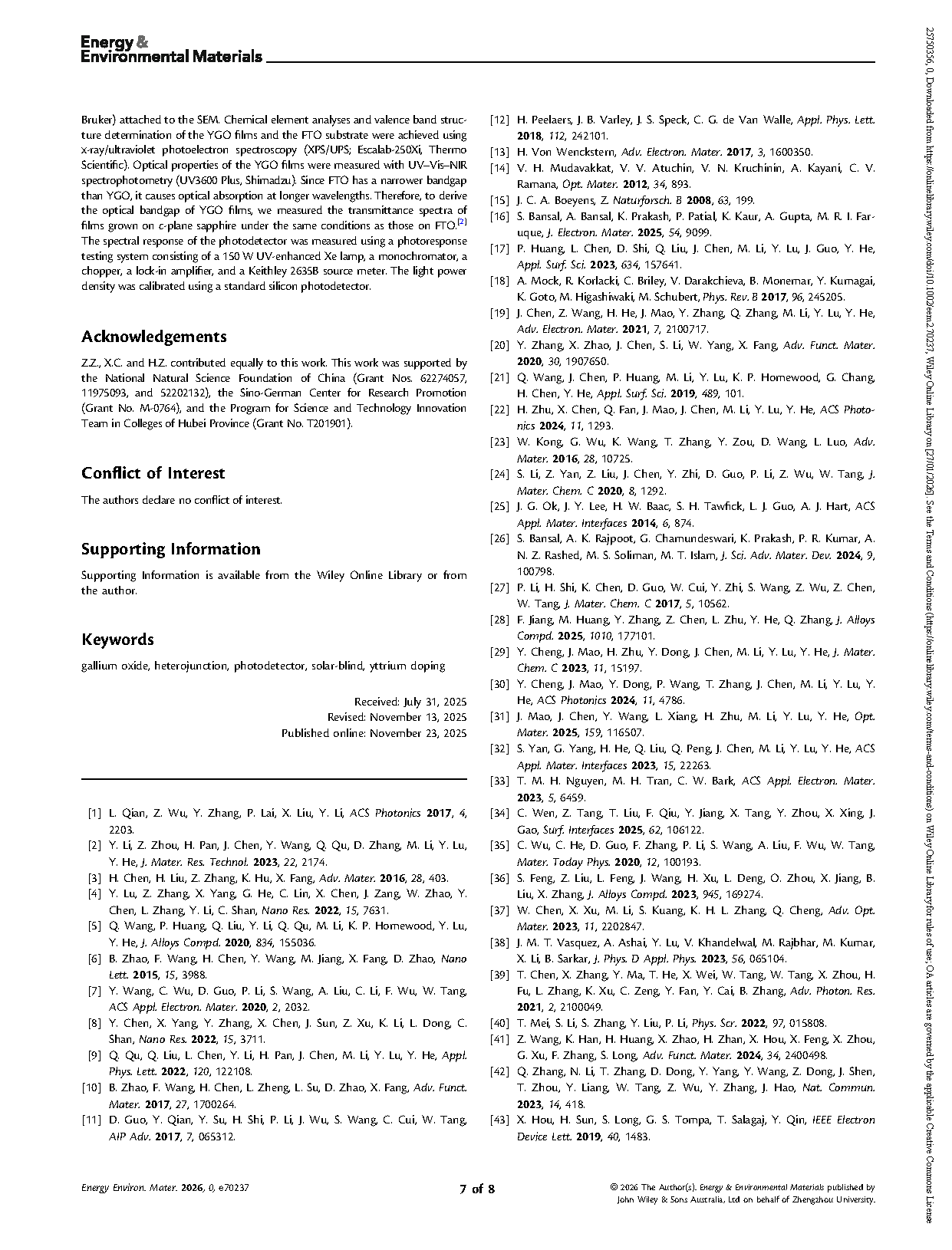
Figure 6 Comparisons of the photoresponse parameters of the Au/YGO/FTO-based photodetectors with other previously reported a) self-driven and b) bias-driven photodetectors.
DOI:
doi.org/10.1002/eem2.70237