Paper Sharing
【Domestic Papers】Transient Charging Dynamics in Stacked Ga₂O₃/ZnO Photovoltaic Units Governing Wavelength-Selective Polarity Switching
日期:2026-02-02阅读:314
Researchers from the Changchun University of Science and Technology have published a dissertation titled "Transient Charging Dynamics in Stacked Ga2O3/ZnO Photovoltaic Units Governing Wavelength-Selective Polarity Switching" in Energy & Environmental Materials.
Project Support
This work was supported by the Jilin Provincial Scientific and Technological Development Program (Grant No. YDZJ202401562ZYTS).
Background
Next-generation photonic technologies, encompassing intelligent sensing, optical computing, and secure communications, are driving a paradigm shift in optoelectronic devices—moving from conventional signal perception to in-situ information processing, often termed in-sensor computing. Central to this shift is the requirement for the device itself to be capable of directly resolving and processing multidimensional optical information—spanning the spectral, temporal, and polarization domains. However, most contemporary photodetector architectures remain “single-modal,” limited to responding to only one dimension: optical intensity. This architectural constraint forces complex processing tasks to be offloaded onto subsequent electronic circuitry, creating inherent latency and power-consumption bottlenecks. Consequently, the development of novel photonic architectures capable of processing multidimensional optical signals directly at the physical device level represents a critical and frontline challenge in the field.
Abstract
Developing self-powered photodetectors capable of processing multi-dimensional optical signals is pivotal for next-generation photonic computing and secure communications. However, conventional device architectures are typically limited to single-mode intensity detection, and the complex photophysics within coupled photovoltaic units remain poorly understood. Here, we reveal a unified “Photovoltaic-Capacitance” coupling mechanism within a vertically stacked, self-powered Ga2O3/PEDOT:PSS and ZnO/Graphene architecture. We demonstrate that the system’s wavelength-selective, transient bipolar response is governed by the multifaceted charging and discharging dynamics between the two coupled units. The key to this mechanism is the ZnO/Graphene (3D/2D) interface, which we define as a novel “Photovoltaic Dynamic-Capacitor” (PDC) component, exhibiting a defined four-stage transient (instantaneous polarization, steady-state saturation, reverse discharge, and relaxation). This architecture enables the Ga2O3 unit (photovoltaic source) to dynamically charge the PDC under 270 nm illumination (+0.27 A/W), while 380 nm illumination directly activates the PDC itself, generating a reverse current (–0.009 A/W). This universal (proven with MgZnO) and dynamically-coupled architecture unlocks a new paradigm for self-powered, multi-dimensional optical processing. We leverage this unique behavior to implement a physical-layer secure communication protocol based on a innovative ternary optical logic (“1”, “0”, “-1”), offering enhanced anti-jamming capabilities rooted in a new photonic degree of freedom.
Conclusion
In summary, this work has elucidated the intrinsic physical mechanism governing the wavelength-selective, transient bipolar response in stacked, self-powered photovoltaic devices. We have demonstrated that this complex behavior is not a simple steady-state competition but is governed by a unified “Photovoltaic-Capacitance” coupling mechanism. The discovery of this mechanism was enabled by our fundamental definition of the ZnO/Graphene 3D/2D interface as a novel PDC, whose distinct four-stage charging and discharging dynamics are the key to the entire system’s operation. We have experimentally validated this model, showing how the Ga2O3 photovoltaic “source” dynamically charges the PDC “load” (positive current), and how the PDC generates a reverse current upon its own activation (negative current). This “Photovoltaic-Capacitance” coupling model, proven to be a universal principle through MgZnO substitution, fundamentally shifts the design paradigm for multi-junction devices—moving beyond static band alignment to embrace transient, dynamic-controlled photonic logic. The successful implementation of a ternary (“1”, “0”, “-1”) optical logic for physical-layer secure communication is a direct demonstration of this new capability. This work opens a new avenue for designing self-powered, multi-dimensional photonic processors where spectral and temporal information can be processed in parallel at the sensor level.
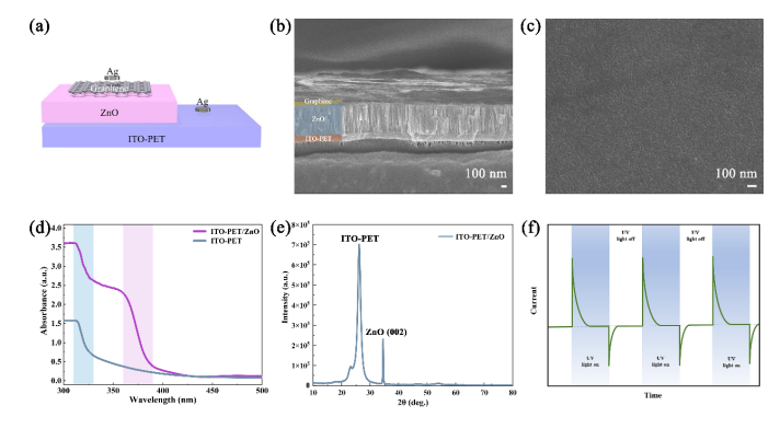
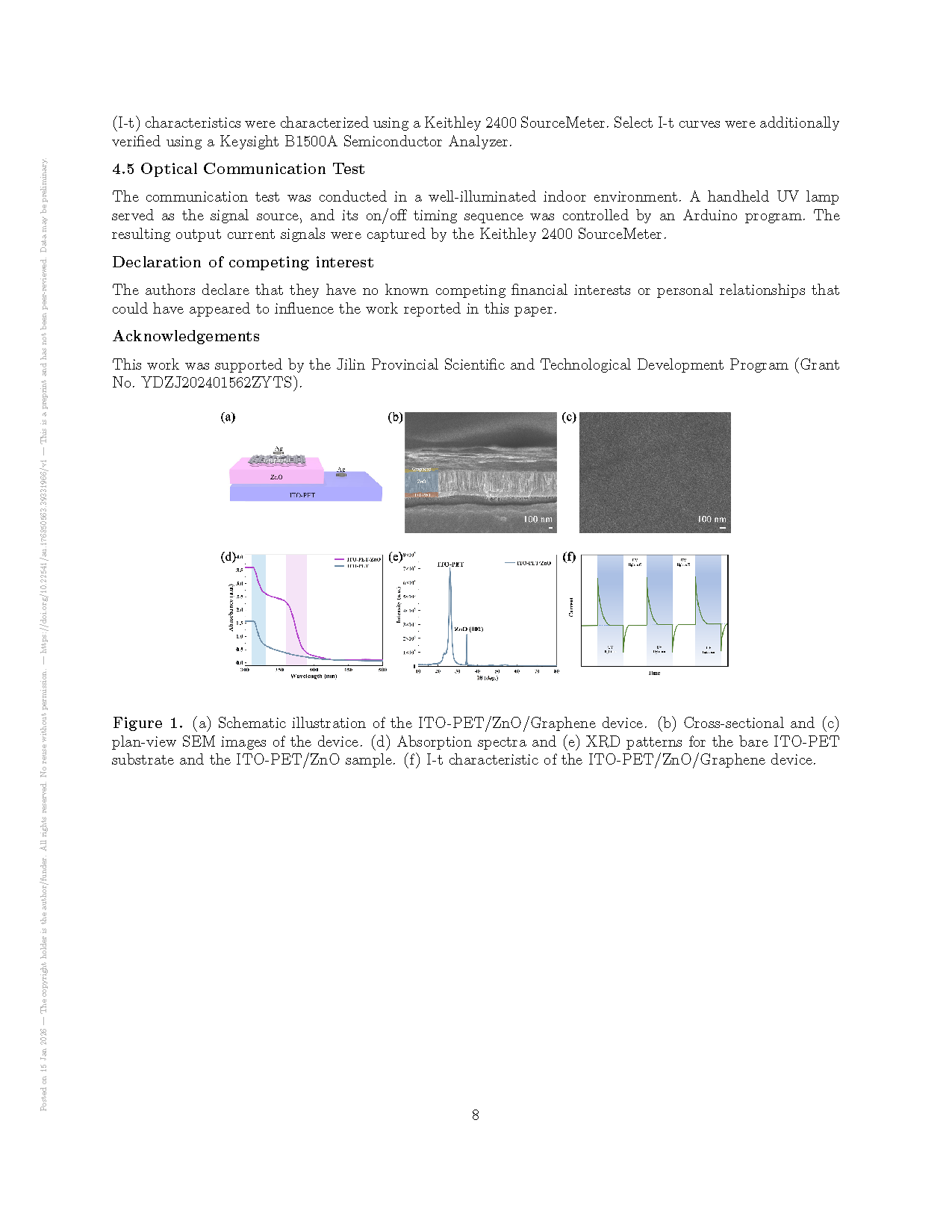
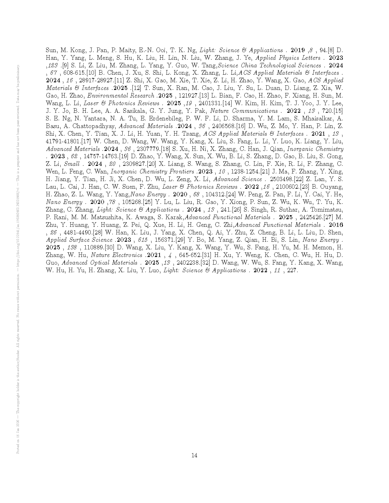
Figure 1. (a) Schematic illustration of the ITO-PET/ZnO/Graphene device. (b) Cross-sectional and (c) plan-view SEM images of the device. (d) Absorption spectra and (e) XRD patterns for the bare ITO-PET substrate and the ITO-PET/ZnO sample. (f) I-t characteristic of the ITO-PET/ZnO/Graphene device.
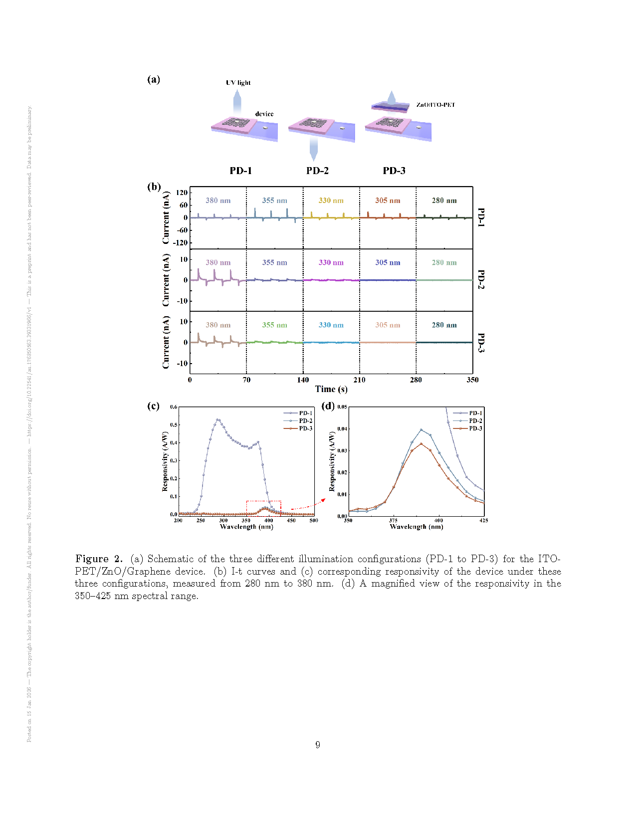
Figure 2. (a) Schematic of the three different illumination configurations (PD-1 to PD-3) for the ITO-PET/ZnO/Graphene device. (b) I-t curves and (c) corresponding responsivity of the device under these three configurations, measured from 280 nm to 380 nm. (d) A magnified view of the responsivity in the 350–425 nm spectral range.
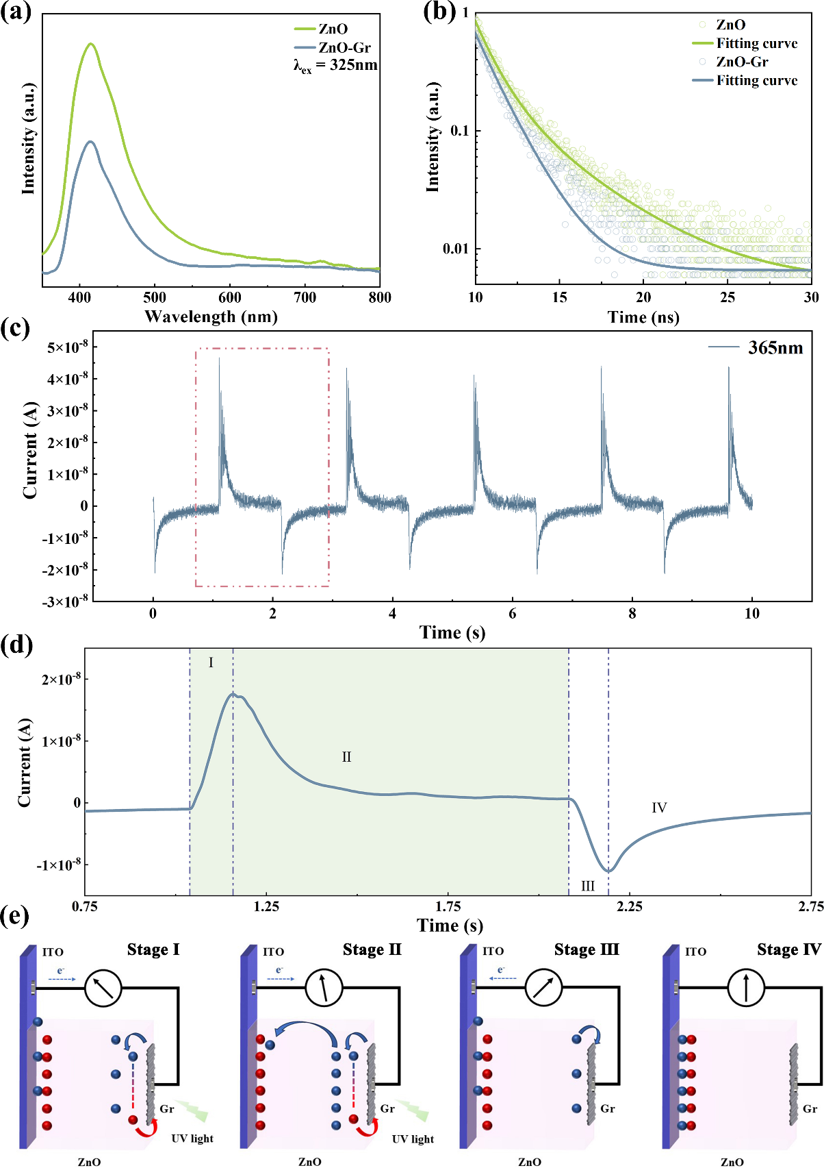
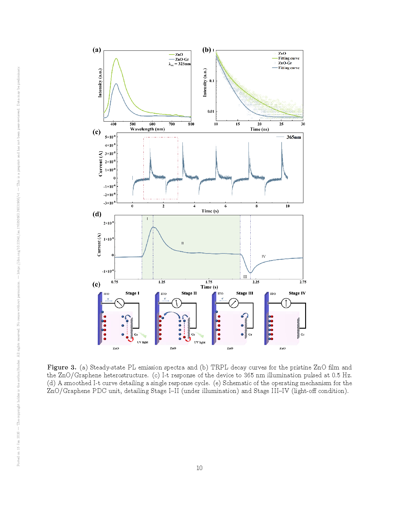
Figure 3. (a) Steady-state PL emission spectra and (b) TRPL decay curves for the pristine ZnO film and the ZnO/Graphene heterostructure. (c) I-t response of the device to 365 nm illumination pulsed at 0.5 Hz. (d) A smoothed I-t curve detailing a single response cycle. (e) Schematic of the operating mechanism for the ZnO/Graphene PDC unit, detailing Stage I–II (under illumination) and Stage III–IV (light-off condition).
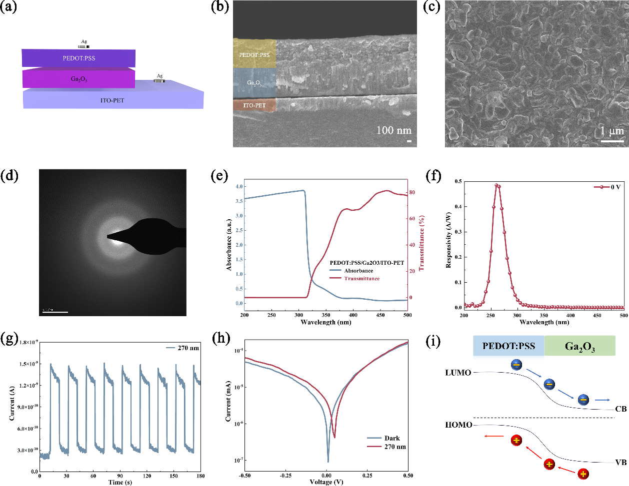
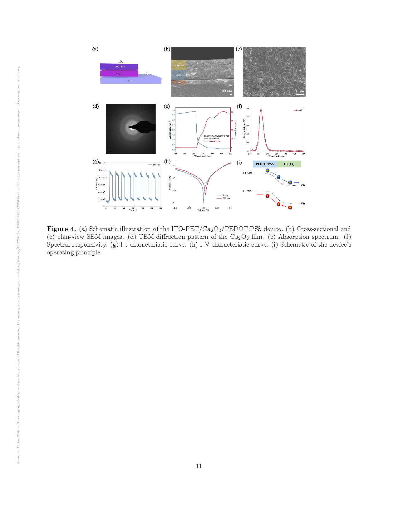
Figure 4. (a) Schematic illustration of the ITO-PET/Ga2O3/PEDOT:PSS device. (b) Cross-sectional and (c) plan-view SEM images. (d) TEM diffraction pattern of the Ga2O3 film. (e) Absorption spectrum. (f) Spectral responsivity. (g) I-t characteristic curve. (h) I-V characteristic curve. (i) Schematic of the device’s operating principle.
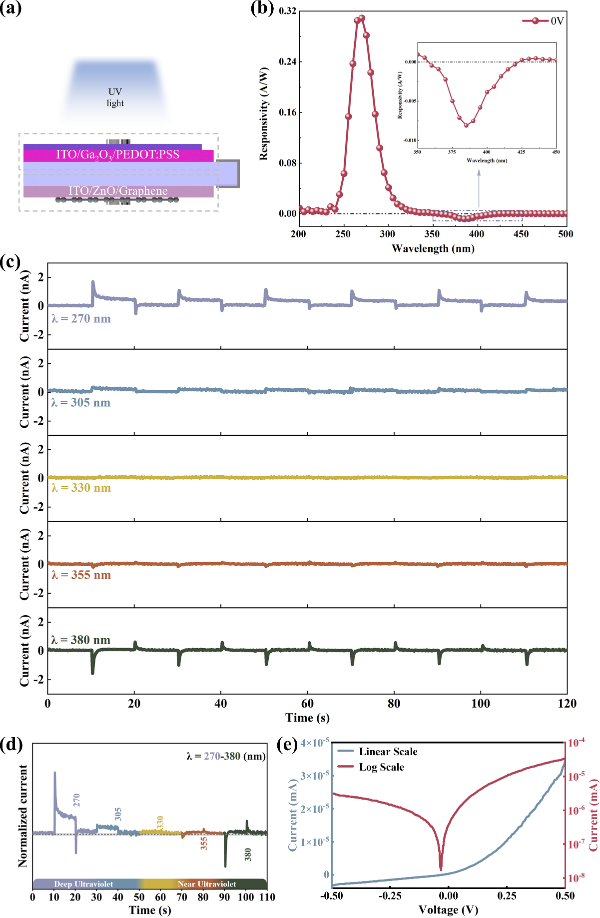
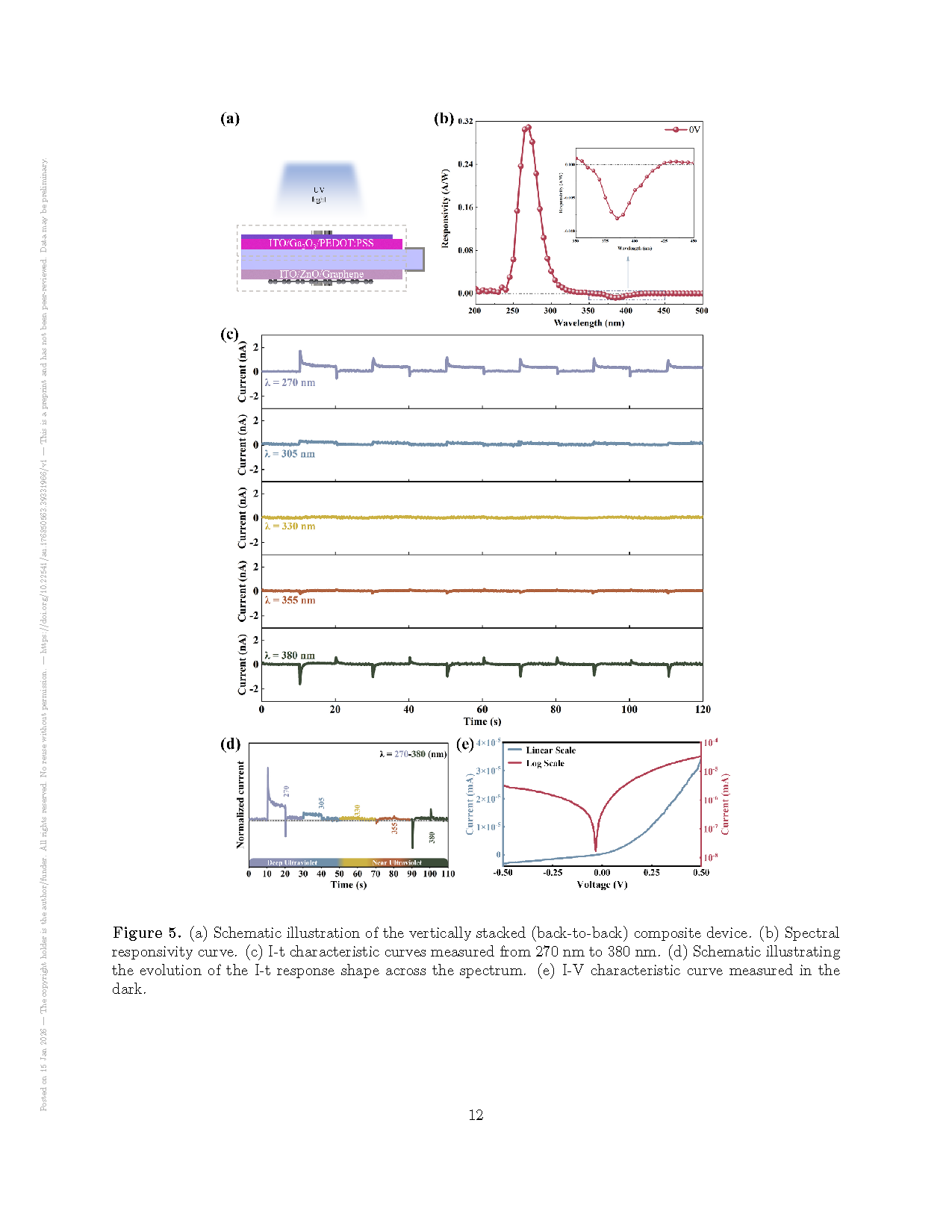
Figure 5. (a) Schematic illustration of the vertically stacked (back-to-back) composite device. (b) Spectral responsivity curve. (c) I-t characteristic curves measured from 270 nm to 380 nm. (d) Schematic illustrating the evolution of the I-t response shape across the spectrum. (e) I-V characteristic curve measured in the dark.
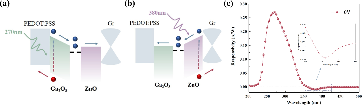
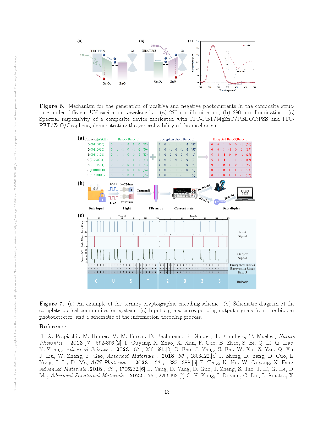
Figure 6. Mechanism for the generation of positive and negative photocurrents in the composite structure under different UV excitation wavelengths: (a) 270 nm illumination; (b) 380 nm illumination. (c) Spectral responsivity of a composite device fabricated with ITO-PET/MgZnO/PEDOT:PSS and ITO-PET/ZnO/Graphene, demonstrating the generalizability of the mechanism.
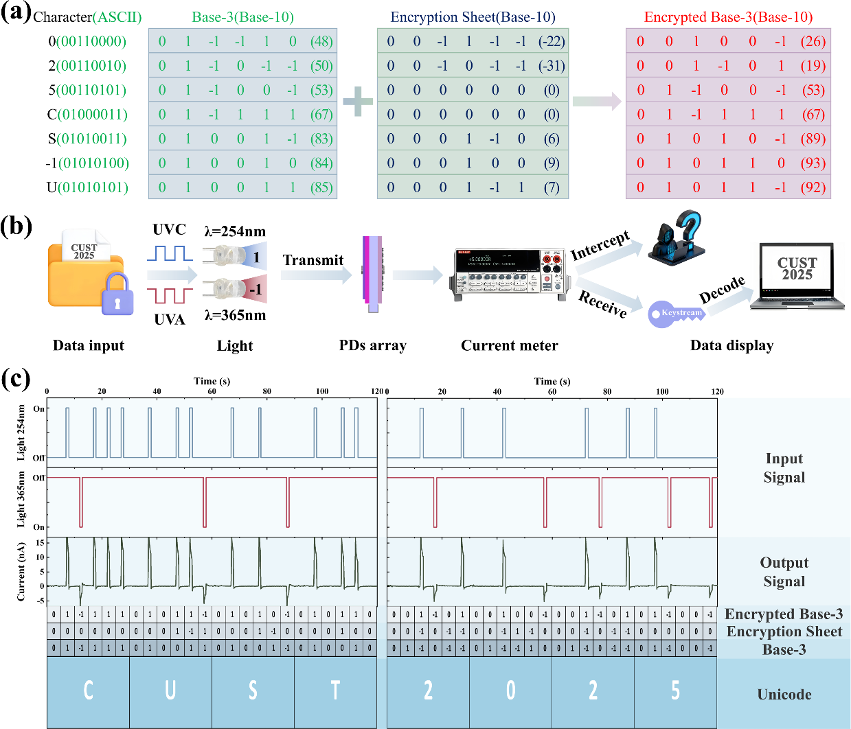
Figure 7. (a) An example of the ternary cryptographic encoding scheme. (b) Schematic diagram of the complete optical communication system. (c) Input signals, corresponding output signals from the bipolar photodetector, and a schematic of the information decoding process.
DOI:
doi.org/10.22541/au.176850563.39331966/v1