


Member News
【Member News】Gallium oxide: The "Key Material" Rewriting the Rules of Semiconductors
日期:2026-02-04阅读:485
In the field of semiconductor materials, silicon-based materials have long dominated. However, with the rapid development of advanced technologies such as 5G communications and electric vehicles, traditional semiconductor materials are approaching their physical limits. According to Science China, third-generation semiconductors represented by silicon carbide and gallium nitride are gaining momentum, while a fourth-generation semiconductor material with even more outstanding performance—Gallium Oxide (Ga₂O₃)—is emerging. As an ultra-wide bandgap semiconductor, Gallium Oxide is triggering a global research surge due to its unique physical properties.
Unique Advantages and Potential of Gallium Oxide
Gallium Oxide has attracted widespread attention primarily because of its exceptional physical properties. Its bandgap reaches as high as 4.9 eV, far exceeding that of silicon (1.1 eV) and silicon carbide (3.3 eV). This ultra-wide bandgap enables Gallium Oxide to withstand higher operating voltages and temperatures, making it particularly suitable for high-power electronic device applications.
Even more striking is its remarkable breakdown electric field strength. Studies indicate that the theoretical breakdown field of Gallium Oxide can reach 8 MV/cm, more than twice that of silicon carbide and gallium nitride. This means that under the same voltage rating, Gallium Oxide devices can be made smaller while achieving higher power density. Experts believe that this characteristic gives Gallium Oxide revolutionary advantages in the field of power electronics.
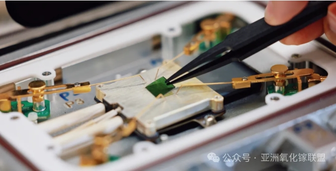
In addition, the growth process of Gallium Oxide single crystals is relatively simple. Unlike silicon carbide, which requires synthesis under high temperature and high pressure, Gallium Oxide can be grown using melt-based methods, significantly reducing production costs. Industry estimates suggest that the cost of Gallium Oxide power devices may be only one-third that of silicon carbide devices, paving the way for future industrialization.
Global Research Landscape and Recent Breakthroughs
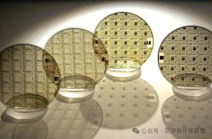
Globally, research on Gallium Oxide is accelerating. In 2023, a collaborative team from the U.S. Air Force Research Laboratory and Kyma successfully developed Gallium Oxide MOSFETs with breakdown voltages exceeding 2,000 volts, achieving significant performance improvements over conventional devices. In Japan, FLOSFIA is focusing on the industrialization of Gallium Oxide power devices and plans to begin mass production in 2025, targeting the electric vehicle charging market.
European research institutions have made important progress in material epitaxy. A novel heteroepitaxial technology developed by the Fraunhofer Institute in Germany has significantly improved the quality of Gallium Oxide thin films, laying the foundation for the development of high-electron-mobility transistors. These international advances indicate the rapid maturation of Gallium Oxide technology.
In China, Gallium Oxide research is also showing strong momentum. Among the leading institutions, the Hangzhou Global Scientific and Technological Innovation Center of Zhejiang University has achieved a series of important results with independent intellectual property, supported by solid fundamental research and innovative technical approaches.
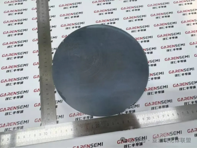
The high cost of Gallium Oxide substrates has severely hindered large-scale applications, while the edge-defined film-fed growth (EFG) method commonly adopted domestically also involves intellectual property risks. Focusing on the key scientific challenges of low-cost and high-quality Gallium Oxide crystal growth, the research team has achieved original and iterative technological breakthroughs, developing a novel melt-based technique with fully independent intellectual property rights—the casting method for bulk Gallium Oxide single crystal growth. Through this “new casting method,” multiple core technologies have been independently developed, enabling large-size and high-speed crystal growth and showing strong potential as a next-generation mass-production technology.
Application Prospects and Future Outlook
The unique properties of Gallium Oxide offer broad application prospects across multiple key fields. In smart grid construction, Gallium Oxide devices can significantly enhance the efficiency and reliability of high-voltage direct current transmission systems. In the new energy vehicle sector, Gallium Oxide power modules are expected to become critical components for 800 V high-voltage platforms, substantially reducing charging time and improving energy utilization efficiency.
The demand for high-power RF devices in 5G and future 6G communication base stations also provides an important arena for Gallium Oxide. Its excellent high-frequency characteristics make it well suited for millimeter-wave communication applications. In the defense and aerospace sectors, the outstanding radiation resistance of Gallium Oxide devices enables reliable operation in extreme environments such as satellites and deep-space probes.
Industry experts predict that as material growth and device fabrication technologies continue to mature, the market for Gallium Oxide power devices will expand rapidly over the next five years. The research team at the Zhejiang University Innovation Center will continue to deepen fundamental research and strengthen industry–academia–research collaboration, focusing on breakthroughs in large-size single crystal growth, device reliability, and system integration, in order to help China gain a strategic advantage in the next generation of semiconductor technologies.
