Paper Sharing
【Member Papers】Solar-blind deep UV photodetector based on β-Ga₂O₃/AlN/p-Si nBp tunneling photodiode for extreme temperature applications
日期:2026-02-05阅读:381
Researchers from the Northeast Normal University have published a dissertation titled "Solar-blind deep UV photodetector based on β-Ga2O3/AlN/p-Si nBp tunneling photodiode for extreme temperature applications" in Materials Today.
Project Support
This work was supported by the National Natural Science Foundation of China under Grant 62274027 and 62404039, the Open Research Fund of Song Shan Lake Materials Laboratory (2023SLABFK03), and 111 Center (B25030), the Postdoctoral Fellowship Program of CPSF (GZC20230416), the Fundamental Research Funds for the Central Universities (2412024QD010).
Background
With the rapidly growing demand for ultraviolet detection in environmental monitoring, military defense, aerospace, and high-voltage power systems under extreme conditions, solar-blind deep-UV photodetectors have attracted increasing attention due to their intrinsically low background noise in the 200–280 nm wavelength range. Compared with conventional technologies such as photomultiplier tubes and silicon-based CCDs, wide-bandgap semiconductor photodetectors offer advantages in miniaturization, integration, and system simplicity. However, commonly studied materials such as AlGaN and MgZnO suffer from phase separation and high defect densities, which significantly limit device performance and reliability.
As an ultra-wide-bandgap semiconductor with a bandgap of ~4.9 eV, β-Ga₂O₃ naturally matches the solar-blind UV spectrum and exhibits excellent thermal, chemical, and radiation stability, making it a promising candidate for next-generation solar-blind photodetectors. In particular, integrating β-Ga₂O₃ with silicon substrates offers the potential to combine high UV sensitivity with mature Si-based technology. Nevertheless, the large lattice mismatch and the presence of an interfacial amorphous SiOx layer severely degrade the crystalline quality of β-Ga₂O₃ films on Si, resulting in high dark current and limited gain performance in Si-based devices.
To overcome these limitations, heterojunction engineering and band alignment modulation have emerged as effective strategies for suppressing dark current and tailoring carrier transport mechanisms. By adjusting the conduction type of the Si substrate and redesigning the heterostructure, it becomes possible to fundamentally alter the dominant gain mechanism and improve device stability over a wide temperature range. Against this background, the present work explores a β-Ga₂O₃/AlN/p-Si heterojunction design, demonstrating a viable pathway toward high-performance, temperature-robust, silicon-based solar-blind UV photodetectors.
Abstract
The authors report high gain solar-blind deep UV photodetector of a β-Ga2O3/AlN/p-Si nBp heterojunction exhibits high-efficiency and stable operation across an extreme temperature range from 173 K to 373 K with ultra-high detectivity of 4.39 × 10¹⁵ – 1.06 × 10¹⁶ Jones as well as high ultraviolet–visible rejection ratio surpassing 105. At room temperature, the nbp device shows a peak responsivity of 18.92 A/W, an extremely high ultraviolet–visible rejection ratio of 6.87 × 10⁵, and a detectivity of 7.38 × 10¹⁵Jones. Upon the application of an external reverse bias voltage of 46 V, a pronounced abrupt increase in the current is observed, signifying the presence of a substantial gain. Under a bias voltage of −70 V, the gain achieves 9 × 10⁴. Variable-temperature I-V characterization reveals that the threshold voltage corresponding to abrupt current onset in the nbp heterojunction exhibits a negative temperature coefficient, which provides the evidence for tunneling effect as the dominant carrier transport mechanism. This operational principle diverges from the avalanche multiplication mechanism reported previously in β-Ga2O3/AlN/ Si nBn heterostructures. Notably, this result demonstrates a design strategy for Si-based β-Ga2O3 solar-blind ultraviolet photodetectors by engineering the Fermi level offset at the β-Ga2O3/Si interface. Through precise modulation of the band alignment, the depletion layer width is controlled, enabling a transition between distinct gain mechanisms.
Conclusion
In this paper, the surface roughness of β-Ga₂O₃ was reduced to 1.7 nm. Based on this, a β-Ga₂O₃/AlN/p-Si nBp heterostructure solar-blind ultraviolet photodetector was constructed. It is proposed that the gain mechanism of the device originates from a tunneling effect. Compared with the β-Ga₂O₃/AlN/n-Si (nBn) structure, a photodetector with a distinct gain mechanism was realized through energy band engineering. At room temperature, the device exhibits a peak responsivity of 18.92 A/W, an ultraviolet–visible rejection ratio (Rpeak/R400nm) as high as 6.87 × 10⁵, and a peak detectivity of 7.38 × 10¹⁵ Jones. In addition, the detector maintains a detectivity on the order of 10¹⁵–10¹⁶ Jones and an ultraviolet–visible rejection ratio exceeding 10⁵ over a wide operating temperature range from 173 K to 373 K. This work provides new insights into the design of Si-based solar-blind photodetectors capable of stable and high-performance operation under extreme temperatures.
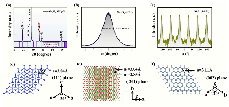
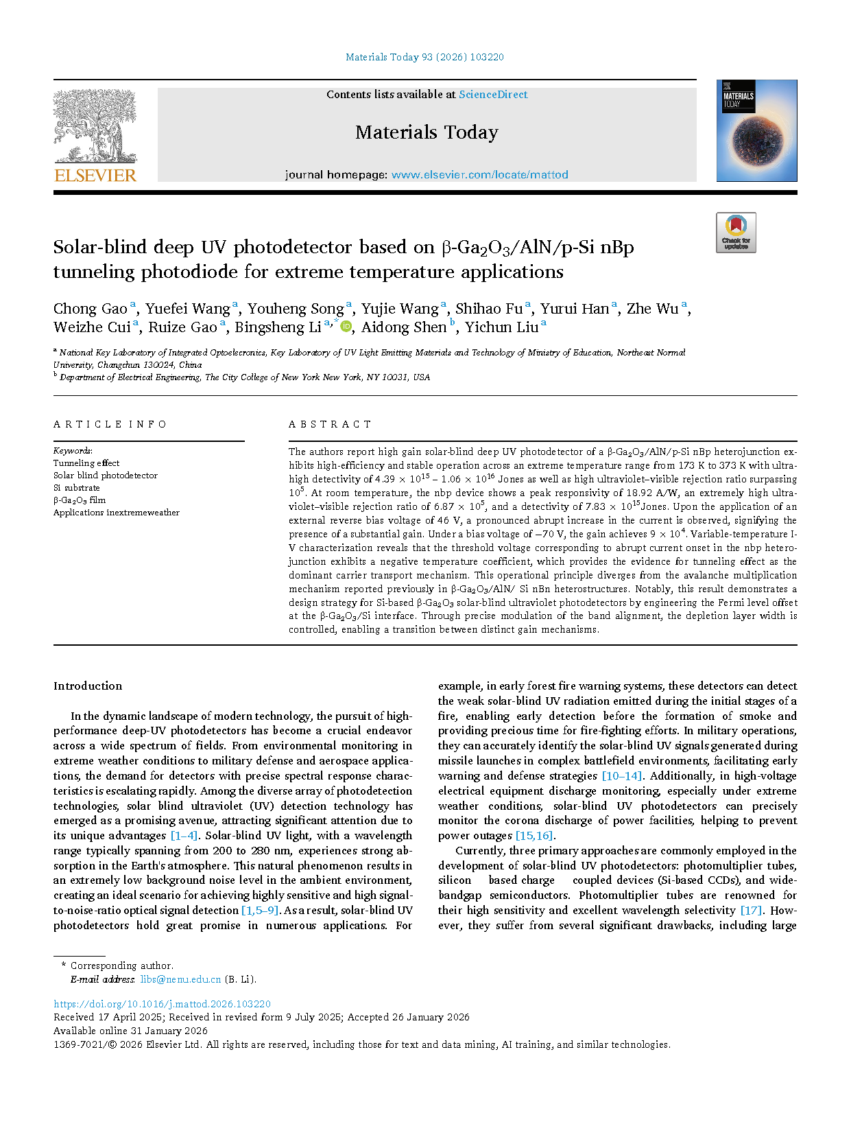
Fig. 1. (a) XRD curves of β-Ga2O3 grown on p-Si (111) with a 30 nm AlN buffer layer. (b) the rocking curve of the (−201) diffraction peak. (c) XRD phi scan of β-Ga2O3 films. the top views of the atomic arrangement of (d) the (−201) plane of β-Ga2O3, (e) the (002) plane of AlN, and (f) the (111) plane of Si arrangement.
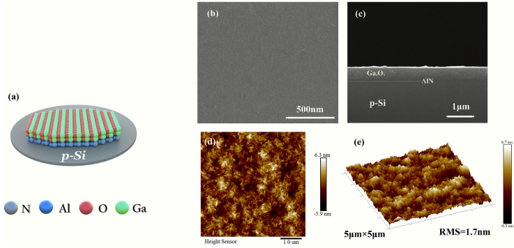
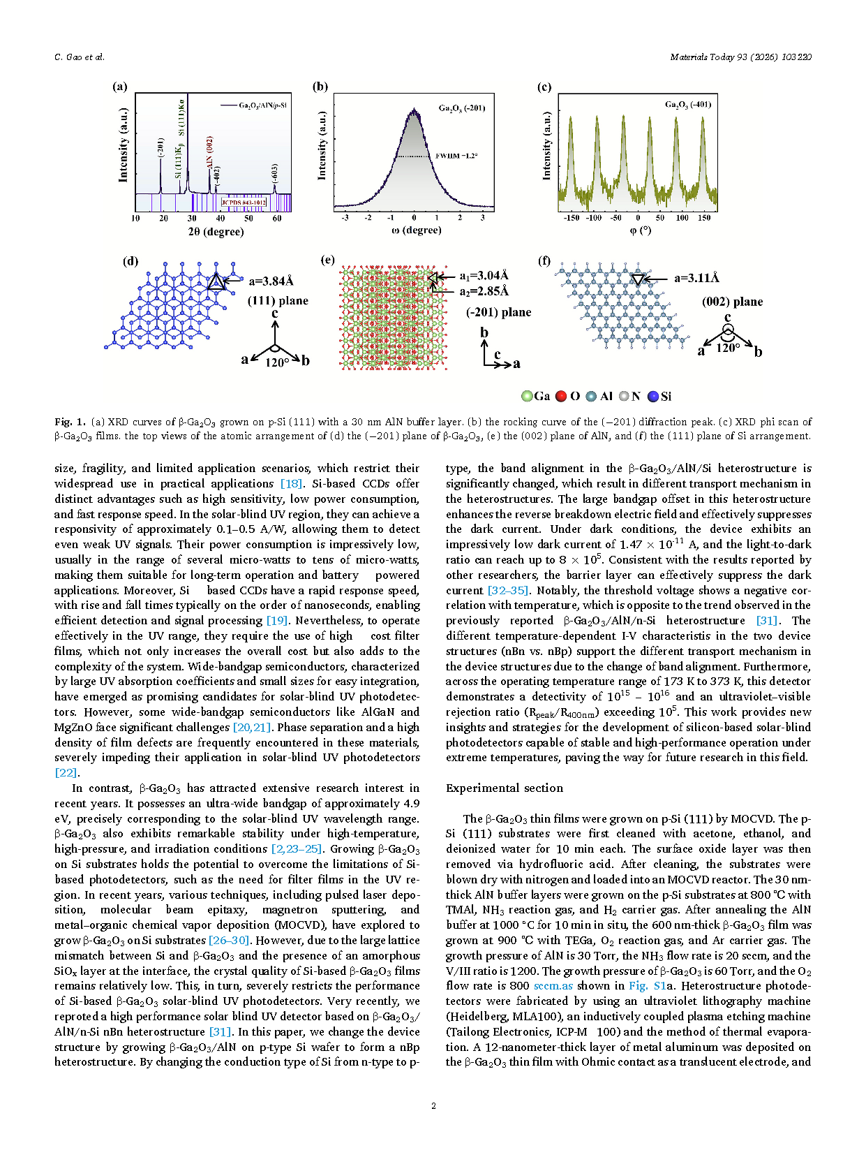
Fig. 2. (a) Schematic diagram of the sample structure. (b) Top-view SEM image of the sample. (c) Side − view SEM image of the sample. (d) 2D atomic force microscope image of the sample within a 5 μm × 5 μm range. (e) 3D atomic force microscope image of the sample within a 5 μm × 5 μm range.
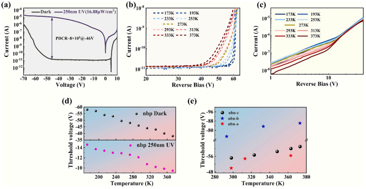
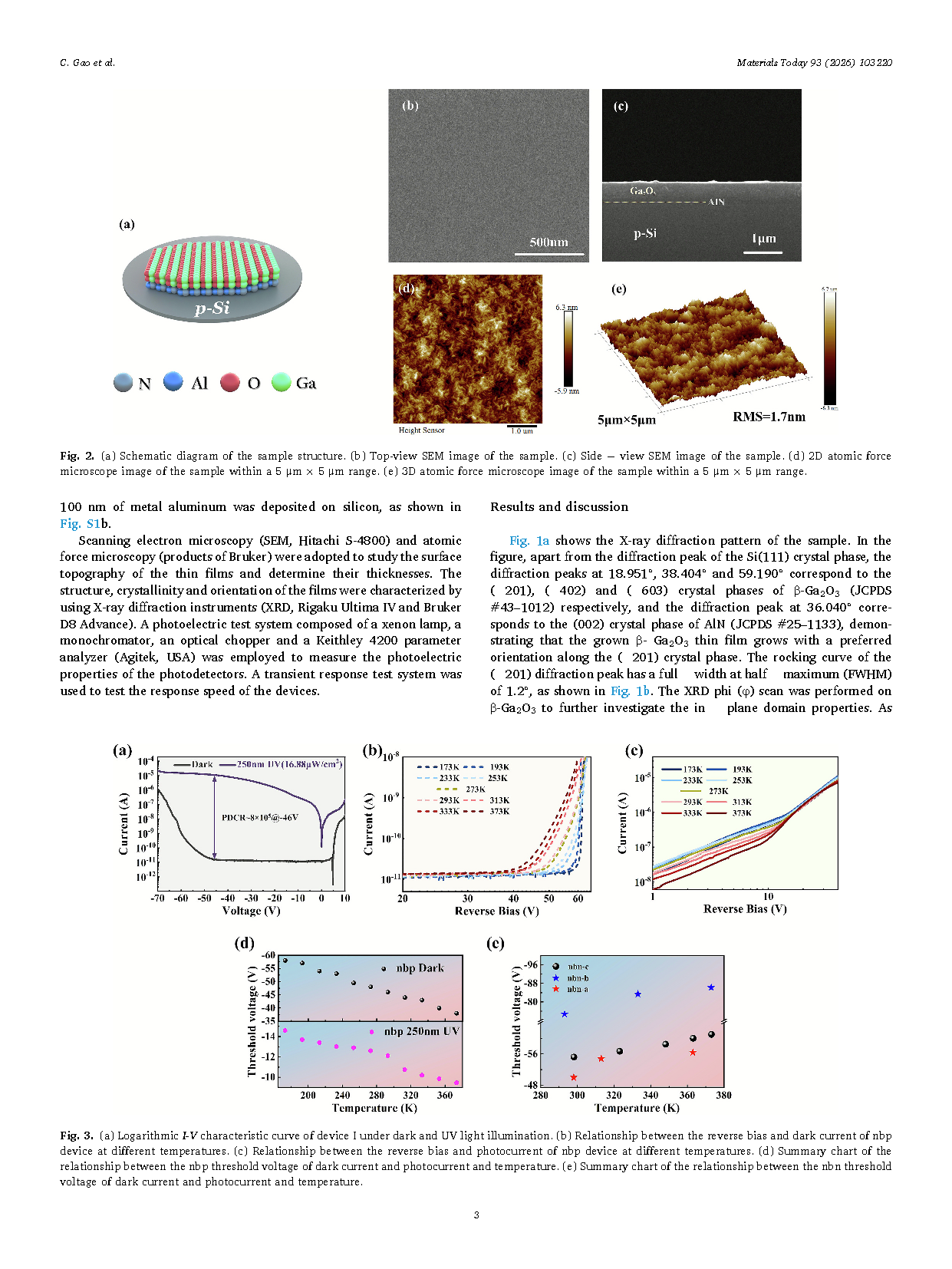
Fig. 3. (a) Logarithmic I-V characteristic curve of device I under dark and UV light illumination. (b) Relationship between the reverse bias and dark current of nbp device at different temperatures. (c) Relationship between the reverse bias and photocurrent of nbp device at different temperatures. (d) Summary chart of the relationship between the nbp threshold voltage of dark current and photocurrent and temperature. (e) Summary chart of the relationship between the nbn threshold voltage of dark current and photocurrent and temperature.
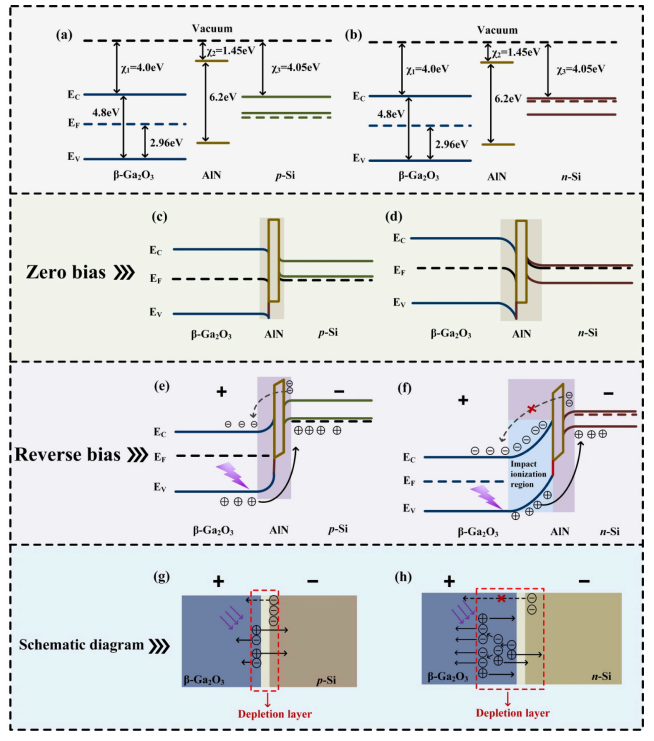
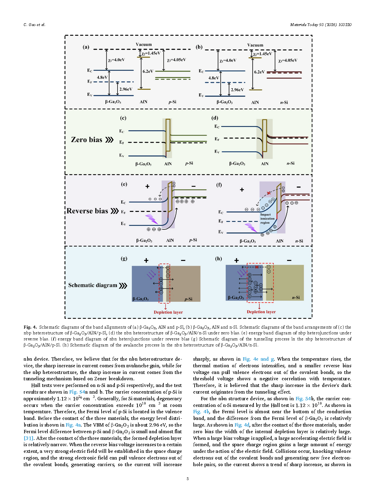
Fig. 4. Schematic diagrams of the band alignments of (a) β-Ga2O3, AlN and p-Si, (b) β-Ga2O3, AlN and n-Si. Schematic diagrams of the band arrangements of (c) the nbp heterostructure of β-Ga2O3/AlN/p-Si, (d) the nbn heterostructure of β-Ga2O3/AlN/n-Si under zero bias. (e) energy band diagram of nbp heterojunctions under reverse bias. (f) energy band diagram of nbn heterojunctions under reverse bias (g) Schematic diagram of the tunneling process in the nbp heterostructure of β-Ga2O3/AlN/p-Si. (h) Schematic diagram of the avalanche process in the nbn heterostructure of β-Ga2O3/AlN/n-Si.
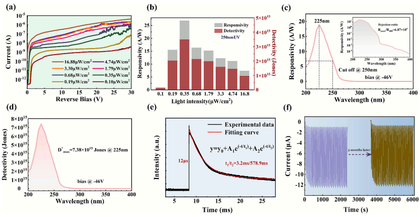
Fig. 5. (a) Reverse I-V characteristics of nbp device under dark and various intensities of 250 nm light illumination. (b) Summary diagram of responsivity and detectivity under 250 nm light illumination with different optical power densities. (c) Spectral response of nbp device at a − 46 V bias (illustration is a logarithmic graph). (d) detectivity of nbp device at a − 46 V bias. (e) Transient response curve of nbp device at a − 46 V bias, and (f) Stability evaluation of the photodetector after three months of storage in open air.
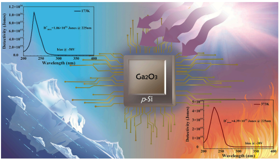
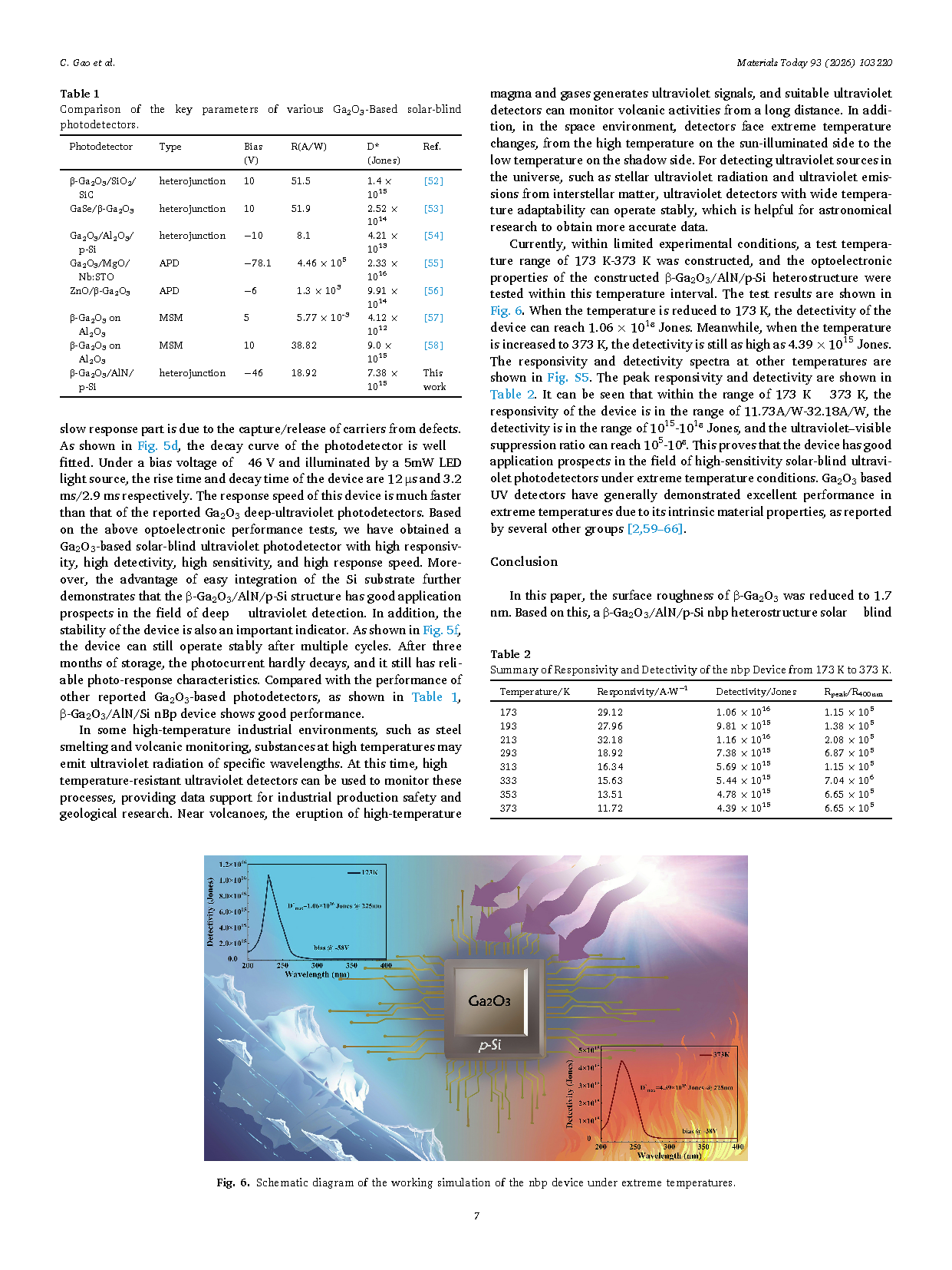
Fig. 6. Schematic diagram of the working simulation of the nbp device under extreme temperatures.
DOI:
doi.org/10.1016/j.mattod.2026.103220