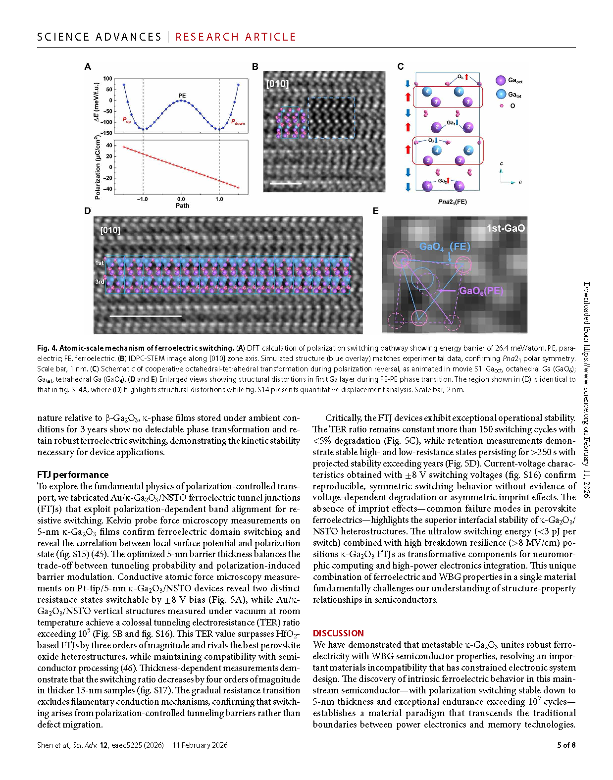
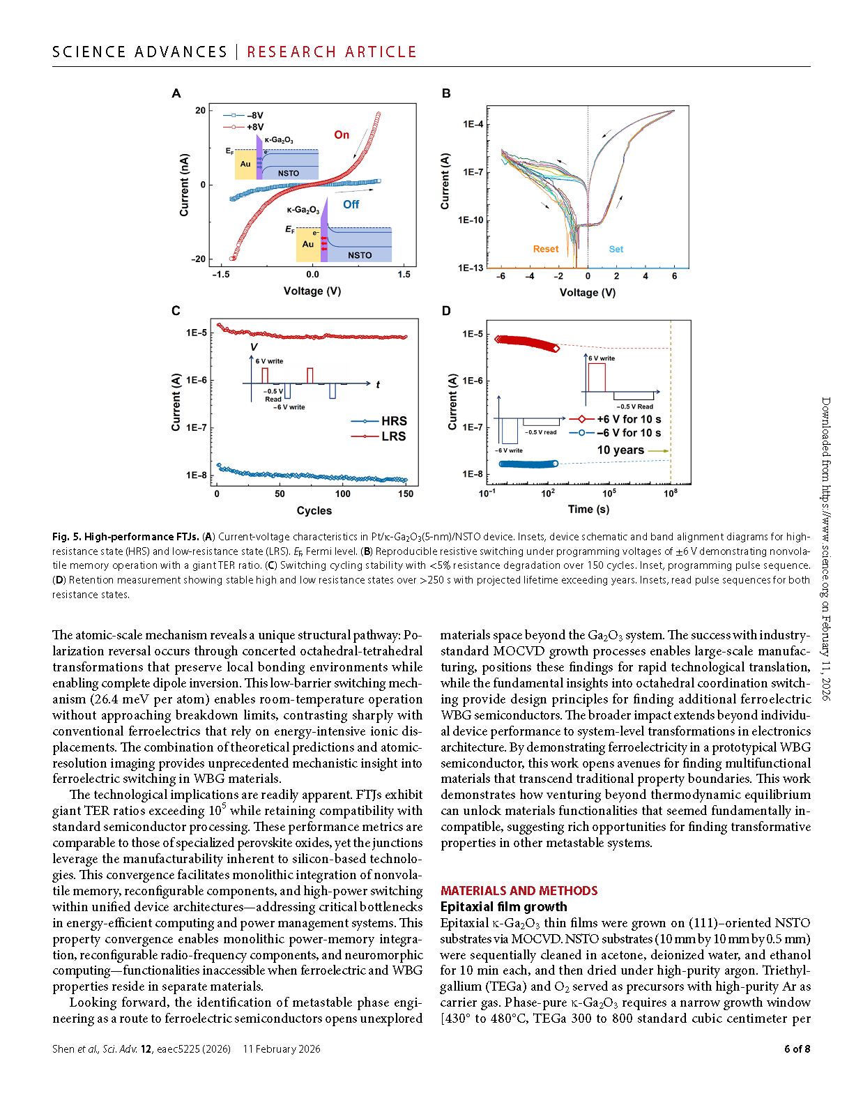
Paper Sharing
【International Papers】Domain engineered gallium oxide phototransistors enabling intelligent ultraviolet vision with dynamic gating
日期:2026-02-12阅读:448
Researchers from the Seoul National University have published a dissertation titled "Domain engineered gallium oxide phototransistors enabling intelligent ultraviolet vision with dynamic gating" in InfoMat.
Background
With the rapid development of machine vision, increasing demands are being placed on real-time performance and energy efficiency in image acquisition and recognition. However, conventional von Neumann architectures suffer from high power consumption and latency due to the physical separation of sensing, memory, and computing units, which makes them particularly unsuitable for edge scenarios where sensing and computation must occur simultaneously. As a result, neuromorphic image sensors that integrate sensing and computation at the device level have attracted growing interest as a promising route toward fast and energy-efficient visual perception. For neuromorphic vision systems, high-selectivity and high–signal-to-noise photodetection is a critical prerequisite. Deep-ultraviolet (DUV) solar-blind detection can inherently suppress interference from visible and ambient light, offering intrinsically high signal-to-noise ratios and enabling reliable operation under complex illumination conditions. Consequently, DUV detection has become an important building block for neuromorphic vision platforms. Among candidate materials, β-Ga₂O₃, an ultra-wide-bandgap semiconductor, stands out due to its wide bandgap, high breakdown field, strong DUV absorption, and excellent thermal stability. Despite these advantages, β-Ga₂O₃-based devices are limited by low carrier mobility, deep trap states, and crystallographic domain boundaries formed during heteroepitaxial growth, which act as scattering centers and trap sites. These intrinsic material and structural issues lead to carrier confinement and persistent photoconductivity (PPC), significantly degrading charge transport and temporal response. Previous studies have mainly relied on circuit-level approaches, such as gate-pulse modulation, to mitigate PPC; however, such strategies do not address the root cause at the material level and often increase system complexity and power consumption. Therefore, there is a clear need for a materials-level solution combined with device and circuit optimization to fundamentally overcome the transport limitations of β-Ga₂O₃. Addressing crystallographic and defect-related issues at the source is essential for realizing high-speed, high-sensitivity, and low-power deep-ultraviolet photodetectors and neuromorphic vision systems.
Abstract
Domain-induced carrier scattering and persistent photoconductivity (PPC) remain major bottlenecks in β-Ga2O3-based deep-ultraviolet (DUV) photodetectors, limiting their use in high-speed imaging, optical communication, and neuromorphic sensing systems. Here, we propose a materials–circuits co-design strategy that integrates crystallographic domain engineering with pulsed-gate modulation to overcome these challenges. Si-doped β-Ga2O3 thin films were epitaxially grown on 6° off-axis sapphire substrates, where atomic step edges induced single-domain alignment, resulting in improved lateral carrier transport and reduced leakage current compared with on-axis counterparts. Under comparable pulsed conditions, single-domain devices exhibited faster recovery than previously reported β-Ga2O3 phototransistors, highlighting the synergistic interplay between domain-engineered transport and dynamic gating. As a result, the devices achieved a high detectivity (D*) of 9.17 × 10¹⁵ Jones and a fast photoresponse of 0.7 ms under reset conditions, while maintaining stable and energy-efficient operation under sub-volt bias. Beyond individual devices, the optimized phototransistors were integrated into a 24 × 24 active-pixel array for system-level DUV imaging. Coupled with convolutional neural networks (CNNs), the array achieved accurate pattern recognition and image reconstruction, while synaptic depression and active reset processes enabled rapid afterimage suppression and image recovery. Overall, this work establishes a domain-engineered, pulse-modulated β-Ga2O3 phototransistor platform that unifies materials-, device-, and system-level innovations, providing a scalable and energy-efficient route toward intelligent ultraviolet vision.
Conclusion
In this study, we implemented a complementary strategy that integrates materials- and circuit-level approaches to address two major bottlenecks in β-Ga2O3-based DUV phototransistors: domain-induced carrier scattering and PPC. Epitaxial growth on off-axis sapphire substrates effectively suppressed rotational domain boundaries, thereby enhancing lateral carrier transport and reducing leakage currents relative to conventional on-axis counterparts. Gate-pulse modulation accelerated carrier recombination and effectively mitigated PPC, leading to sub-millisecond response. When integrated into a 24 × 24 active pixel phototransistor array, the optimized devices enabled high-contrast DUV imaging and accurate CNN-based pattern recognition under sequential illumination. Beyond achieving a D* of 9.17 × 10¹⁵ Jones and a 0.7 ms response time, this work underscores that domain engineering and dynamic gate modulation together provide an effective framework for scalable and intelligent UWBG optoelectronics, providing a practical foundation for real-time neuromorphic ultraviolet vision. Importantly, synaptic depression further allowed clear image reconstruction under sub-volt operation, underscoring the feasibility of low-power neuromorphic sensing. Furthermore, the coexistence of reset and residual-depression functionalities underscores the adaptive nature of domain-engineered β-Ga2O3 phototransistors, which can flexibly adapt between rapid-reset operation for fast recovery and residual-depression operation for energy-efficient recognition, depending on the system requirements .
Building upon these results, we further explored how dynamic gate control can be extended toward more compact array-level operation through a bipolar photogate pulsing scheme. Owing to the wide bandgap and highly insulating nature of the domain-engineered β-Ga2O3, the Iph can be effectively modulated even without auxiliary switching transistors, demonstrating an inherent material-driven advantage that enables stable on/off control and simplified circuit design. Alternating positive and negative pulses stabilized Iph dynamics, with positive pulses suppressing PPC and negative pulses enabling selective pixel access through current modulation, thereby offering clear benefits in integration density, energy efficiency, and process scalability. These advances underscore the synergistic value of combining material- and circuit-level design, positioning β-Ga2O3 phototransistors not only as high-performance DUV detectors but also as versatile building blocks for neuromorphic sensing. Taken together, our findings establish domain-engineered, pulse-driven β-Ga2O3 phototransistors as a scalable and energy-efficient platform for next-generation ultraviolet vision, paving the way for integration into multifunctional neuromorphic and optoelectronic systems.
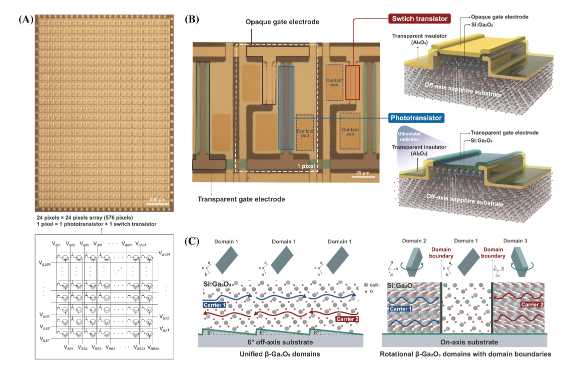
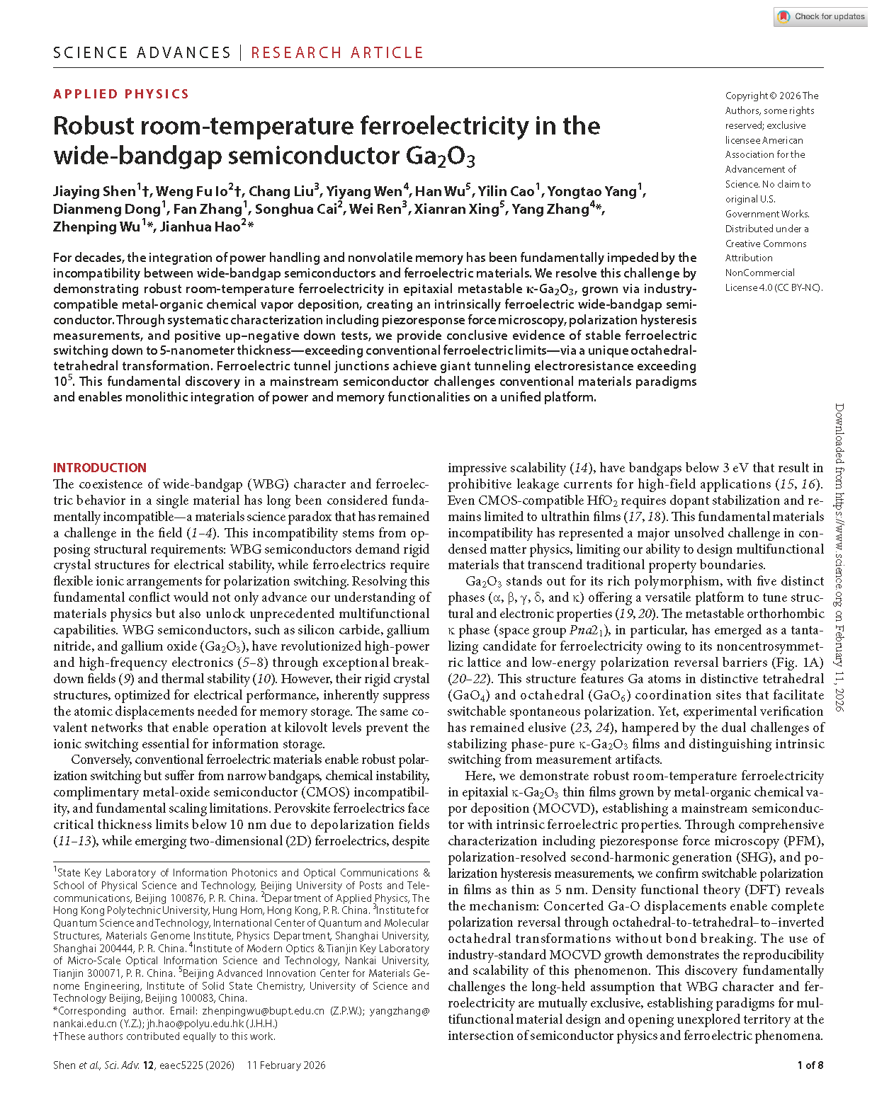
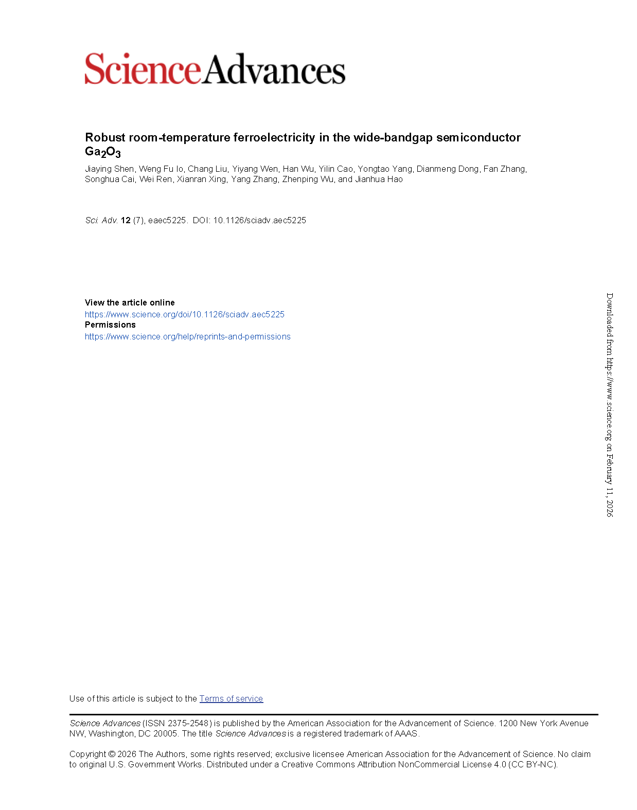
FIGURE 1 Scalable integration of Si:Ga2O3 phototransistors into active pixel phototransistor arrays with controlled domain orientation. (A) Optical microscopy image (top) and corresponding circuit diagram (bottom) of a 24 × 24 active pixel phototransistor array, comprising 576 pixels. Each pixel integrates a phototransistor and a switch transistor, which are individually addressed via dedicated Vdd, Vss, Vg,p, and Vg,s voltage lines. (B) Magnified optical image of a single pixel (left) and schematic diagrams of the vertical stack structures (right) for both transistors. The phototransistor utilizes a transparent gate electrode to allow DUV exposure, while the switch transistor uses an opaque gate to block light. (C) Schematic illustration of domain formation on on-axis versus off-axis sapphire substrates. The symmetric on-axis surface induces rotational domains with boundaries that hinder carrier transport, while the stepped off-axis surface promotes single-domain alignment and improved mobility.
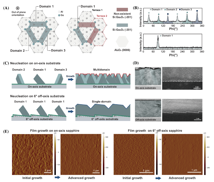
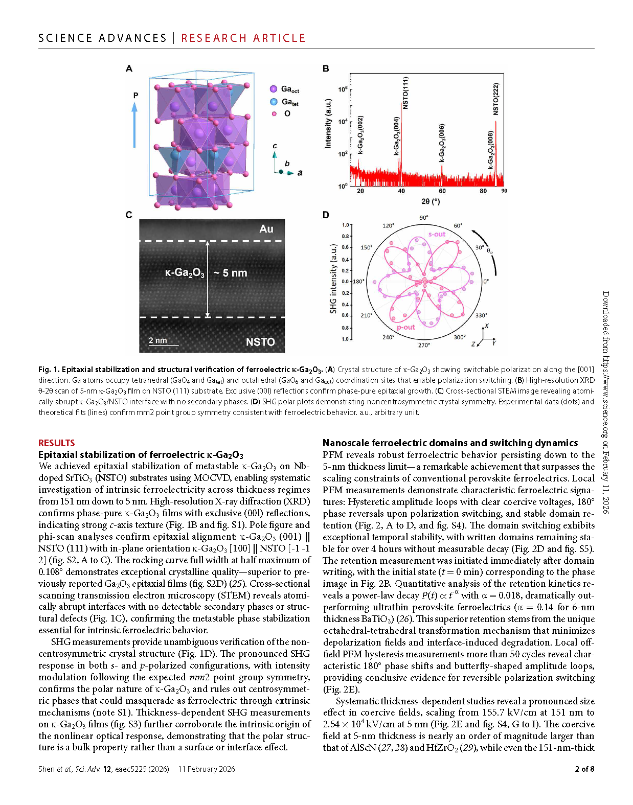
FIGURE 2 Structural control of Si:Ga2O3 thin films via off-axis sapphire substrate. (A) Schematic illustration of domain growth on on-axis substrate with a flat surface and 6° off-axis substrate with a stepped morphology. During film growth, the 6° off-axis substrate restricts the domain growth direction. (B) φ-scan measurements showing a single, well-defined peak for the 6° off-axis substrate, attributed to controlled domain alignment. (C) Schematic representation of the film growth orientation from a cross-sectional perspective, illustrating that a unified domain structure results in a smoother surface morphology compared to multidomain growth. (D) Cross-sectional TEM image showing that, unlike on-axis substrate, the 6° off-axis substrate exhibits a smoother surface with single-crystal growth along the steps. (E) AFM images illustrating the morphological evolution during film growth, demonstrating that the off-axis substrate maintains lower surface roughness.
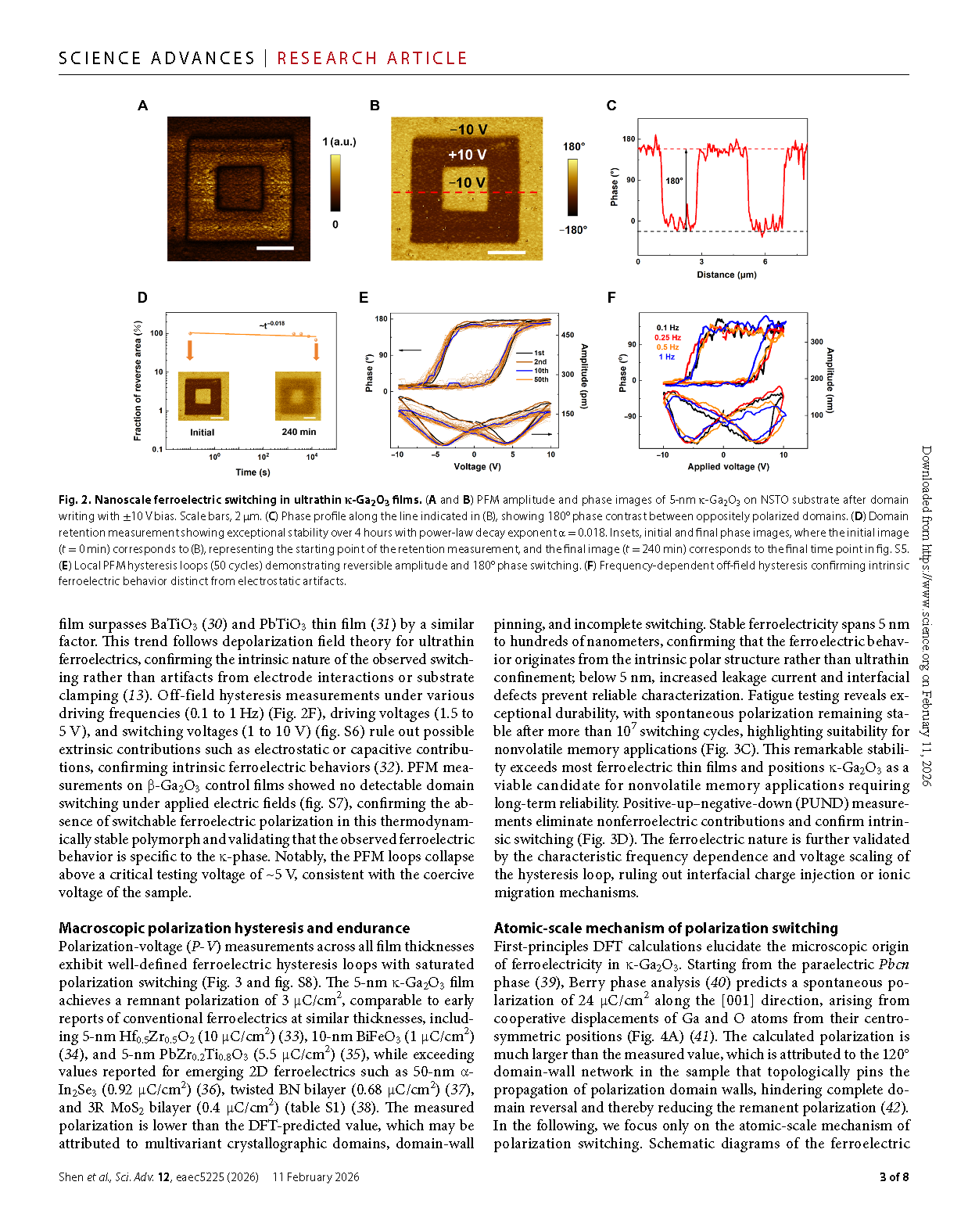
FIGURE 3 Characterization and performance of the phototransistor. (A) Ilight, (B) R, and (C) D* as functions of Vg,p and Plight. (D) D* as a function of Vg,p under a Plight of 110 μW cm–2, showing that D* is maximized when the photogating effect is pronounced and Idark is minimized. (E) Time-resolved Ilight measurements under varying Plight for the single-domain phototransistor illustrating a highly stable and reproducible Ilight response to DUV illumination. (F) ΔVth as a function of Plight for Si:Ga2O3-based multidomain and single-domain phototransistors. (G) D* of single-domain and multidomain phototransistors showing the consistently superior performance of the single-domain device. (H) R as a function of DUV wavelength showing that the single-domain device exhibits significantly higher photoresponse efficiency than its multidomain counterpart and demonstrates a distinct peak response at 254 nm. (I) Time-resolved current response under pulsed drain bias in single-domain and multidomain Si:Ga2O3 devices. (J) The normalized TRPL decay profiles showing the defect density related carrier dynamics.
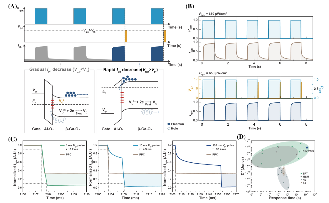
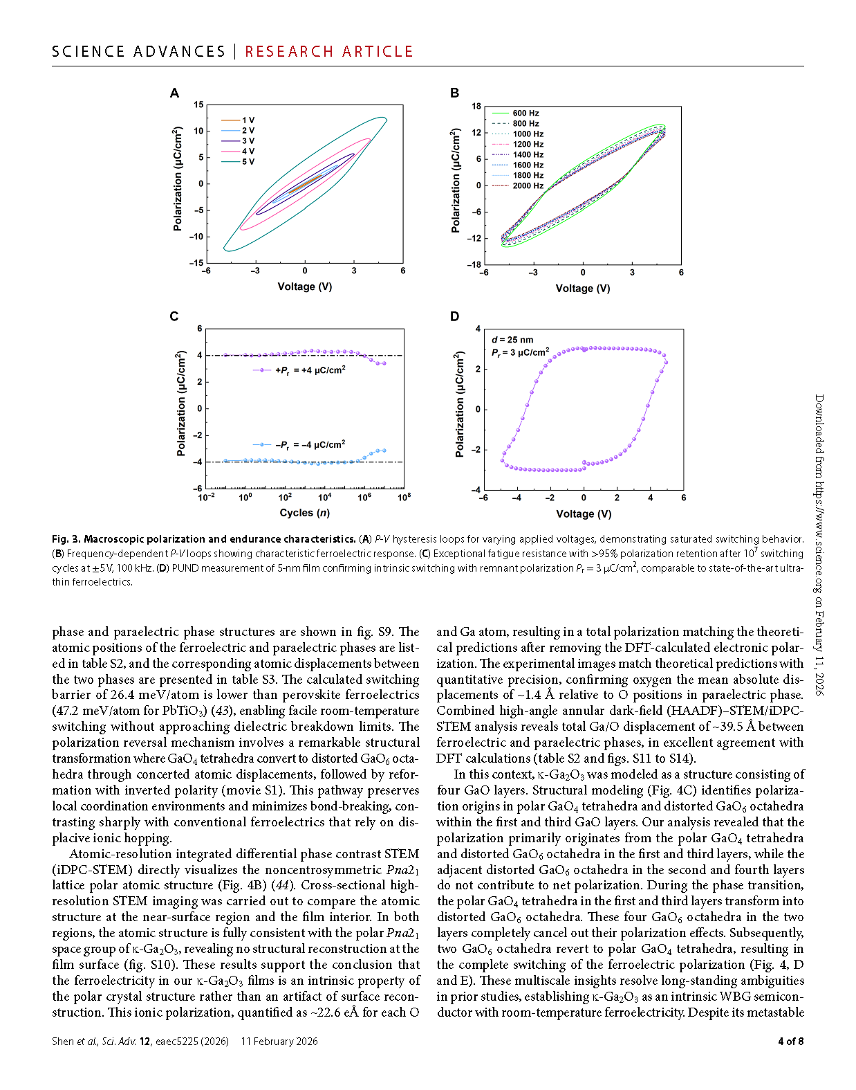
FIGURE 4 Effective elimination of PPC in phototransistors through Vg,p pulsing. (A) Experimental schematic illustrating the PPC elimination process, including DUV pulse irradiation, Vg,p pulse application, and Ilight measurement, along with an energy band diagram describing the PPC removal mechanism via an electric pulse applied to the photogate. The Vg,p pulse induces electron accumulation, effectively suppressing PPC. (B) Effect of Vg,p pulse on PPC removal. The top panel shows the Ilight response to a DUV pulse without gate pulsing, while the bottom panel demonstrates effective PPC suppression when a positive Vg,p pulse is applied under identical conditions. (C) Measurement of response decay time as a function of Vg,p pulse width. (D) Performance comparison of photodetectors in terms of D* and response time. The PPC elimination mechanism enables a shorter response time and enhanced D* compared to conventional photosensors.
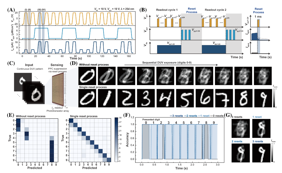
FIGURE 5 Pattern recognition under continuous DUV illumination with Vg,p-induced PPC elimination. (A) Time-resolved Ilight measurements under four operation modes (I–IV), showing the isolated and combined effects of DUV illumination and switch transistor gating. (B) Quasi-parallel readout protocol with row-wise sensing and reset implemented through Vg,p-pulse modulation (left), and suppression of residual Iph following Vg,p pulsing during the reset process (right). (C) Active pixel phototransistor array operation under continuous DUV illumination for sequential digit (0–9) recognition. (D) Terminal current maps of each session under continuous DUV exposure, demonstrating that the reset process effectively removes residual afterimages across different digit classes. (E) Confusion matrices comparing recognition performance with and without the reset process during sequential digit exposure. (F) Recognition accuracy across digit sessions with 0–3 applied Vg,p reset pulses, showing delayed convergence in the absence of reset and markedly improved accuracy when reset pulses are introduced. (G) Current map evolution at the onset of digit presentation as a function of the number of reset pulses applied between digits.
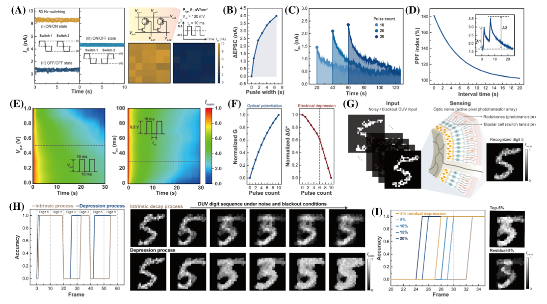
FIGURE 6 Synaptic characteristics of phototransistors and energy-efficient pattern recognition under low-light noisy and blackout conditions. (A) Schematic of Iph modulation by switch transistors. Waveforms of the applied Vg,s1 and Vg,s2 are shown (left), and applying ±500 mV, 10 ms Vg,s pulses produces three distinct current levels controlled by two switch transistors (right). Potentiation characteristics of the phototransistor. (B) Excitatory postsynaptic current as a function of pulse width, (C) Ilight responses with increasing pulse number, and (D) PPF curve. (E) Depression characteristics of the phototransistor. Current maps showing depression modulated by pulse amplitude (left) and by inter-pulse interval (right). (F) Conductance modulation curves illustrating optical potentiation and electrical depression. (G) Active pixel phototransistor array operation for digit recognition, highlighting synapse-like sensing. Even under noisy and blackout DUV inputs, clear digit images are reconstructed. (H) Recognition accuracy and current maps under sequential DUV exposure of the digit sequence 5–5–3–3–5–5. Depression Vg,p pulses were applied to the top 15% of high-current pixels. (I) Recognition performance for digit “3” in the third session under varying percentages of depressed pixels. The residual-depression method demonstrates superior efficiency, enabling clearer recognition even with only 5% depressed pixels.
DOI:
doi.org/10.1002/inf2.70112