Paper Sharing
【Member Papers】Ultrahigh Dielectric Permittivity in Ultrathin 2D β-Ga₂O₃ for Advanced Dielectric Applications
日期:2026-02-12阅读:424
Researchers from the Fudan University have published a dissertation titled "Ultrahigh Dielectric Permittivity in Ultrathin 2D β-Ga2O3 for Advanced Dielectric Applications" in Nano Letters.
Project Support
This work was supported in part by the Fundamental Research Funds for the Central Universities of Ministry of Education of China (No. D5000240188), in part by the Natural Science Foundation of Jiangsu Province (Grants No. BK20240484), and in part by the Natural Science Foundation of Shandong Province (Grant No. ZR2025QC1603).
Background
As advanced transistors continue to scale into the nanometer regime, maintaining strong gate control to suppress short-channel effects while simultaneously reducing operating voltage for low-power consumption has become a central challenge in the semiconductor industry. Conventional silicon dioxide (SiO₂) gate dielectrics are approaching their fundamental physical limits, as aggressive thickness scaling leads to severe quantum tunneling leakage and increased power dissipation. Replacing SiO₂ with high-permittivity (high-k) dielectrics is therefore essential for sustaining device scaling, since high-k materials enable a larger physical thickness at the same equivalent oxide thickness (EOT), effectively suppressing leakage currents and enhancing gate capacitance for improved channel control.
At present, hafnium oxide (HfO₂)-based dielectrics are widely adopted owing to their compatibility with CMOS fabrication processes; however, their dielectric constant is typically limited to around 50, which may be insufficient for future technology nodes requiring more aggressive scaling. Although some materials, such as relaxor ferroelectrics, can exhibit higher permittivity, their dielectric performance often degrades significantly in ultrathin films due to interfacial layer effects, severely restricting practical implementation. These limitations highlight the urgent need for novel dielectric materials that combine a higher dielectric constant with robust performance at the ultrathin limit. In this context, β-gallium oxide (β-Ga₂O₃), an ultrawide-bandgap semiconductor known for its excellent physical and chemical stability, has attracted increasing attention, yet its dielectric properties in the two-dimensional (2D) ultrathin regime remain largely unexplored.
In this work, we address this gap by systematically investigating the dielectric behavior of ultrathin 2D β-Ga₂O₃ single crystals. Metal–insulator–metal capacitors based on a 10 nm-thick β-Ga₂O₃ flake are fabricated, revealing an anomalously high dielectric constant of approximately 150. Through combined photoelectric and microstructural analyses, the physical origin of this ultrahigh permittivity is elucidated, and the strong potential of ultrathin β-Ga₂O₃ for high-performance memory and logic applications is demonstrated. These results establish β-Ga₂O₃ as a highly promising high-k dielectric material in the 2D limit for next-generation electronic devices.
Abstract
The continuous scaling of semiconductor devices necessitates the integration of high-permittivity (high-k) dielectrics to maintain gate control and reduce power consumption. Here, we report an ultrahigh dielectric constant (k) of ∼150 in ultrathin (10 nm) β-gallium oxide (β-Ga2O3) metal–insulator–metal capacitors. Photoresponse and microstructural analyses link the giant permittivity to an oxygen vacancy (VO)-ordered phase. The fabricated capacitors exhibit excellent performance for memory applications, including low dielectric loss (<0.02 at 100 kHz), low leakage current (<10–7 A/cm2), high operating speed (>20 MHz), and high endurance (>1010 cycles). To validate practical utility, MoS2 field-effect transistors gated by β-Ga2O3 were fabricated, exhibiting a high on/off ratio (>106), a low subthreshold swing (SS) of 68.1 mV/dec, negligible hysteresis (5.8 mV), and ultralow gate leakage (∼10–13 A). These findings establish ultrathin β-Ga2O3 as a compelling high-k material for next-generation logic and memory devices.
Conclusion
In summary, we have fabricated and characterized MIM capacitors based on an ultrathin (10 nm) 2D β-Ga2O3 dielectric, discovering an ultrahigh dielectric constant of ∼150. Photoelectric and microstructural analyses strongly suggest that this giant permittivity originates from the formation of an ordered oxygen vacancy superstructure, which induces a new polar phase with large dipole moments. The capacitor demonstrates performance that is promising for memory applications, including low dielectric loss, low leakage current, high operating speed (>20 MHz), and high endurance (>1010 cycles). We also have demonstrated MoS2 FETs gated by an ultrathin β-Ga2O3 dielectric with promising performance metrics: high on/off ratio, near-ideal SS, negligible hysteresis, and ultralow leakage current. This work not only reveals the notable dielectric properties of β-Ga2O3 in the 2D limit but also suggests it is a promising high-k material for future memory and logic technologies.
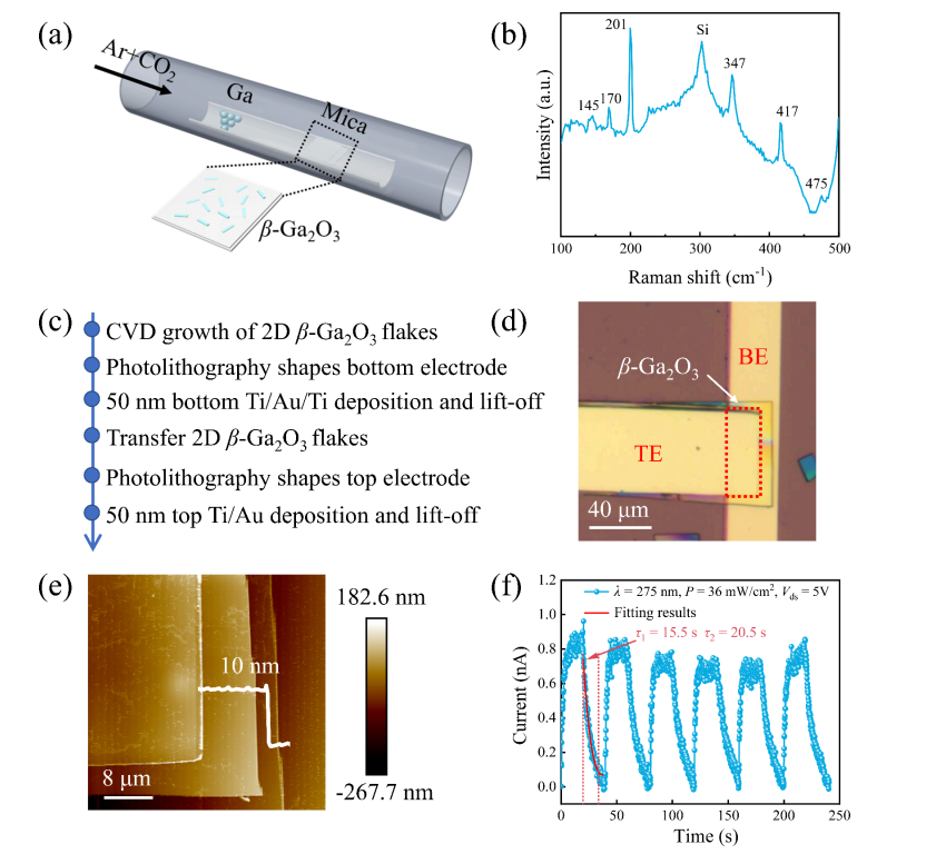
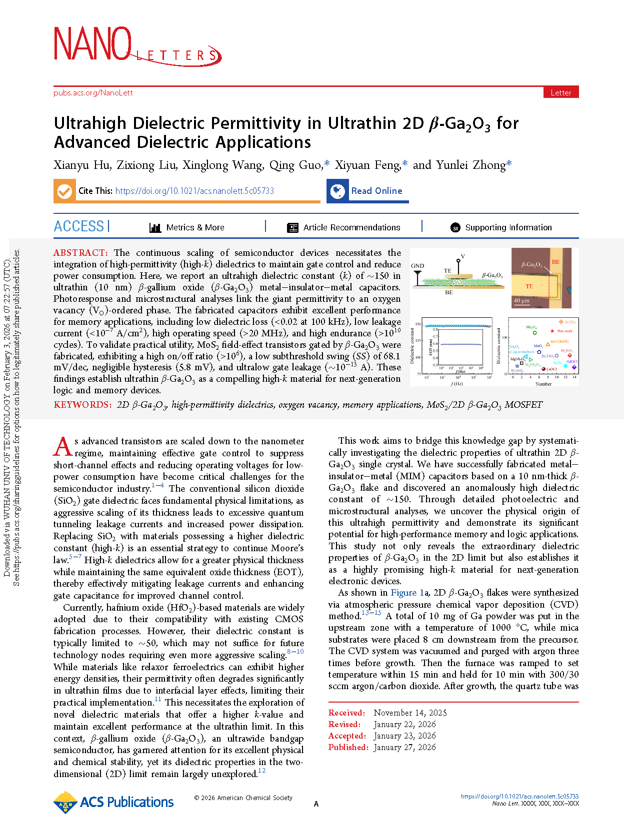
Figure 1. Fabrication, characterization, and electrical performance of the β-Ga2O3 MIM capacitor. (a) Synthesis schematic illustration of β-Ga2O3 flakes grown on mica. (b) Raman spectra of β-Ga2O3 flakes on Si/SiO2 substrate. (c) Schematic illustration of the key fabrication steps for the MIM capacitor based on a β-Ga2O3 dielectric layer. (d) Top-view optical microscopy image of the completed capacitor device. (e) AFM image illustrating the surface morphology. (f) I−t characteristics of the β-Ga2O3 capacitor measured under dark and illuminated conditions.
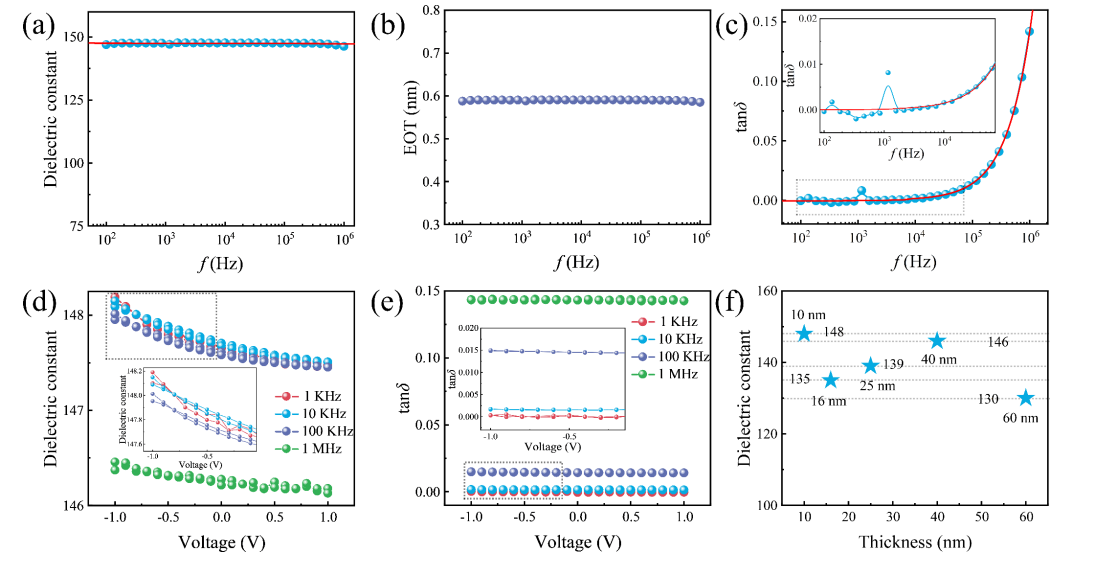
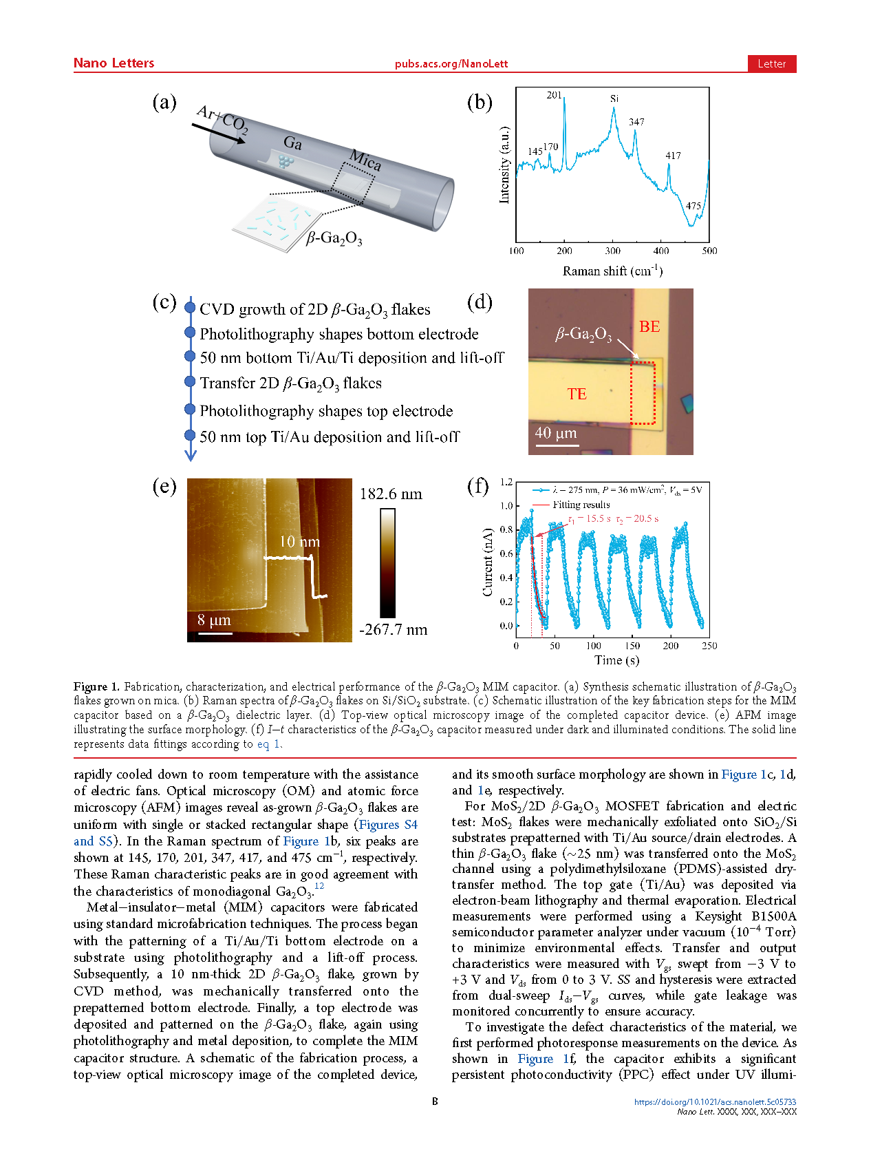
Figure 2. Dielectric properties of the β-Ga2O3 capacitor. (a, b) Frequency dependences of the dielectric constant (ε′, a) and the equivalent oxide thickness (EOT, b) under an oscillating field of VOSC = 0.05 V. The solid line represents data fittings according to eq 2. (c) Corresponding frequency dependence of the loss tangent (tan δ). The solid line represents data fittings according to eq 3. Inset: A magnified view of the lowfrequency section. (d and e) Voltage dependences of ε’ and tan δ, respectively, measured at frequencies of 1 kHz, 10 kHz, 100 kHz, and 1 MHz. Inset: Local magnification images. (f) Dielectric constants of MIM capacitors with different thicknesses ranging from 10 to 60 nm at a measuring frequency of 1 MHz.
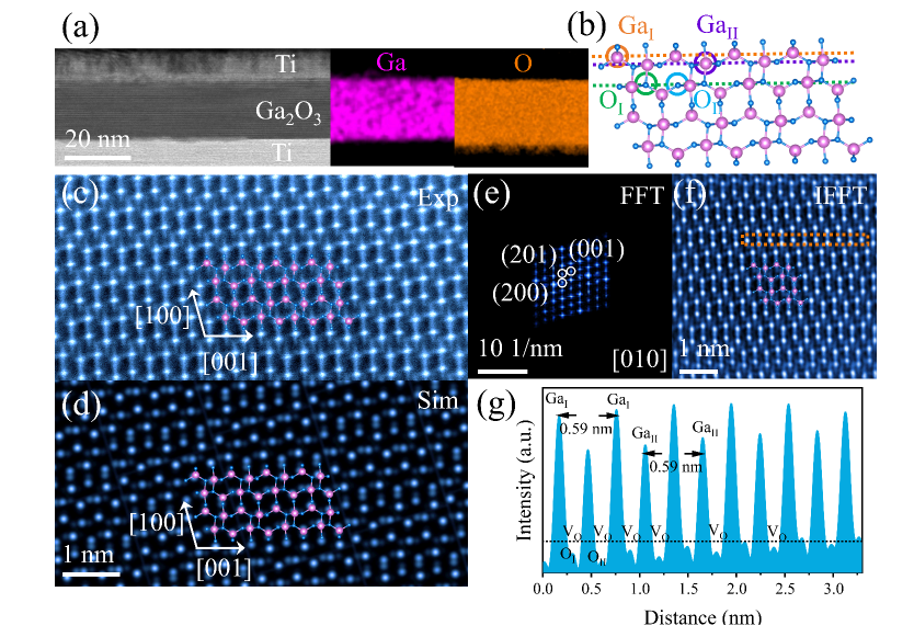
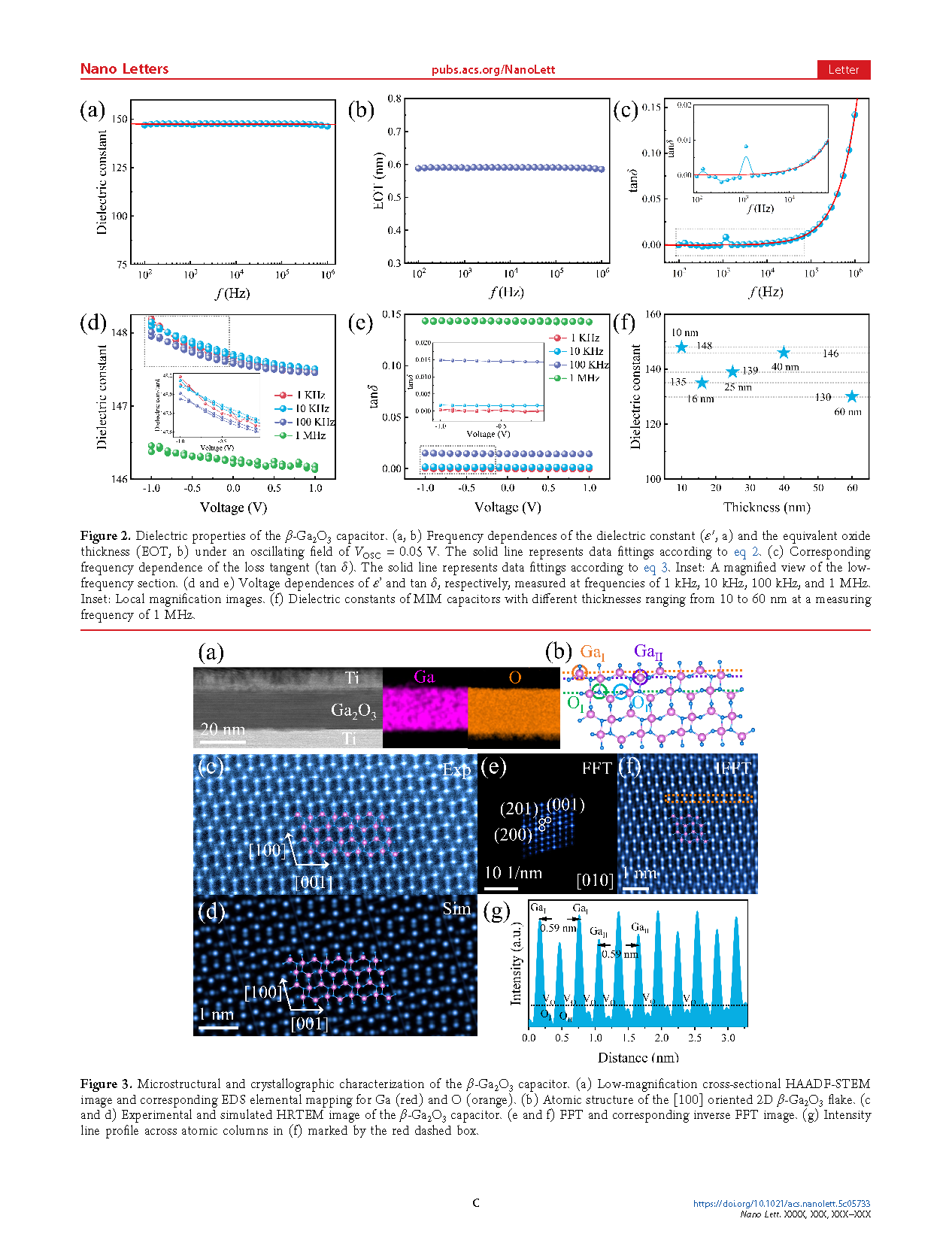
Figure 3. Microstructural and crystallographic characterization of the β-Ga2O3 capacitor. (a) Low-magnification cross-sectional HAADF-STEM image and corresponding EDS elemental mapping for Ga (red) and O (orange). (b) Atomic structure of the [100] oriented 2D β-Ga2O3 flake. (c and d) Experimental and simulated HRTEM image of the β-Ga2O3 capacitor. (e and f) FFT and corresponding inverse FFT image. (g) Intensity line profile across atomic columns in (f) marked by the red dashed box.
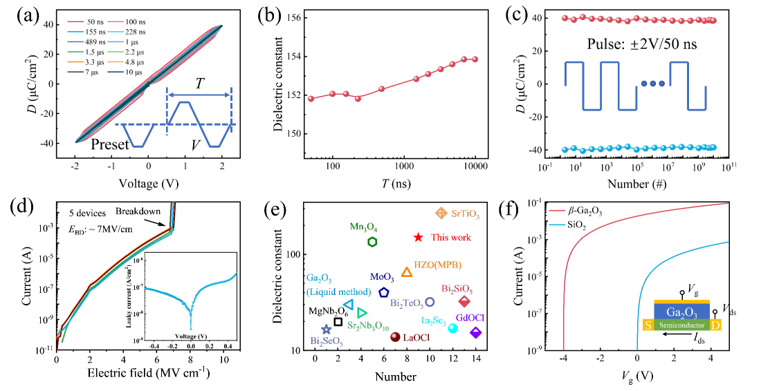
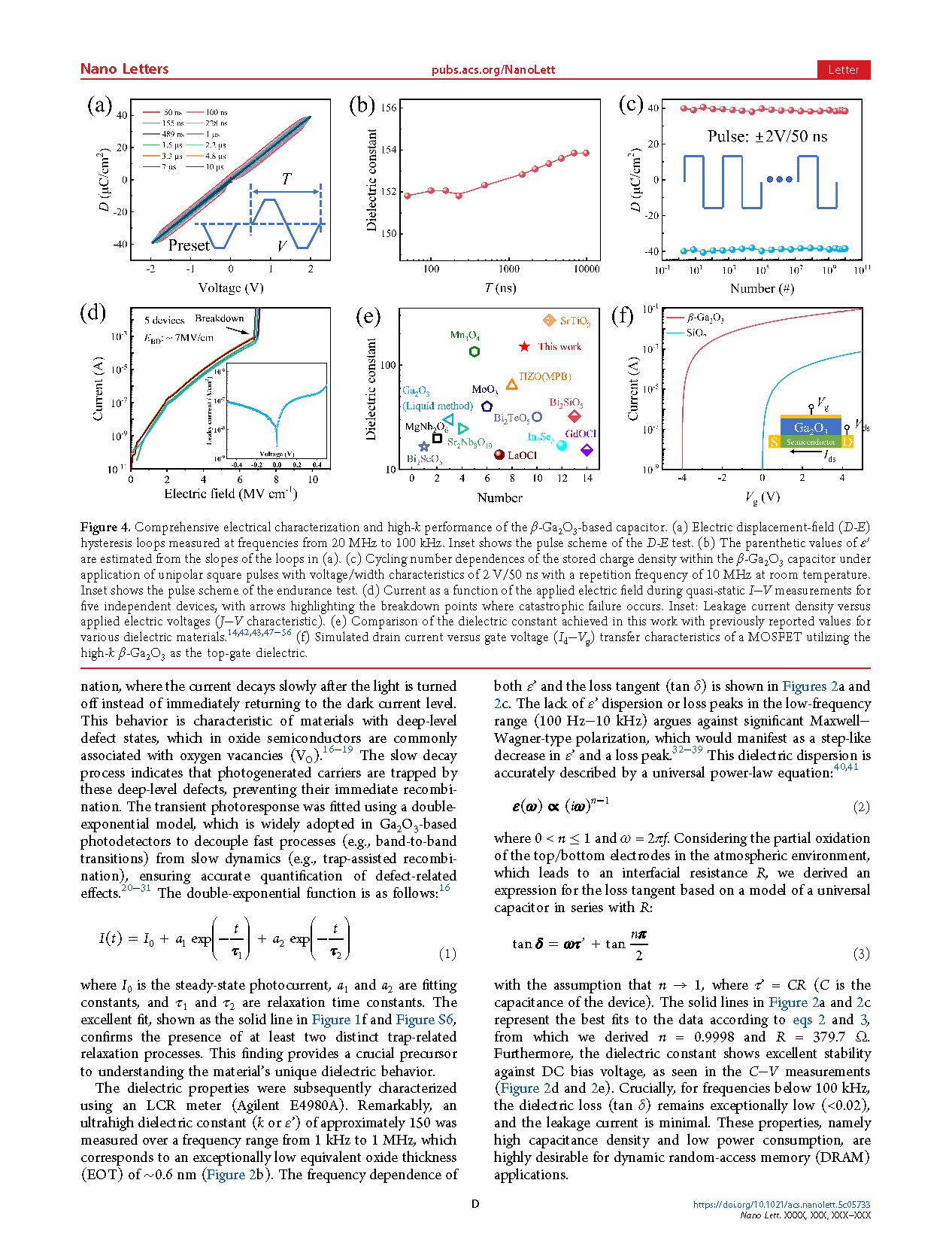
Figure 4. Comprehensive electrical characterization and high-k performance of the β-Ga2O3-based capacitor. (a) Electric displacement-field (D-E) hysteresis loops measured at frequencies from 20 MHz to 100 kHz. Inset shows the pulse scheme of the D-E test. (b) The parenthetic values of ε′ are estimated from the slopes of the loops in (a). (c) Cycling number dependences of the stored charge density within the β-Ga2O3 capacitor under application of unipolar square pulses with voltage/width characteristics of 2 V/50 ns with a repetition frequency of 10 MHz at room temperature. Inset shows the pulse scheme of the endurance test. (d) Current as a function of the applied electric field during quasi-static I−V measurements for five independent devices, with arrows highlighting the breakdown points where catastrophic failure occurs. Inset: Leakage current density versus applied electric voltages (J−V characteristic). (e) Comparison of the dielectric constant achieved in this work with previously reported values for various dielectric materials. (f) Simulated drain current versus gate voltage (Id−Vg) transfer characteristics of a MOSFET utilizing the high-k β-Ga2O3 as the top-gate dielectric.
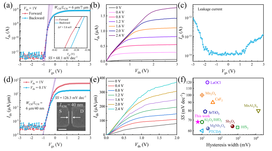
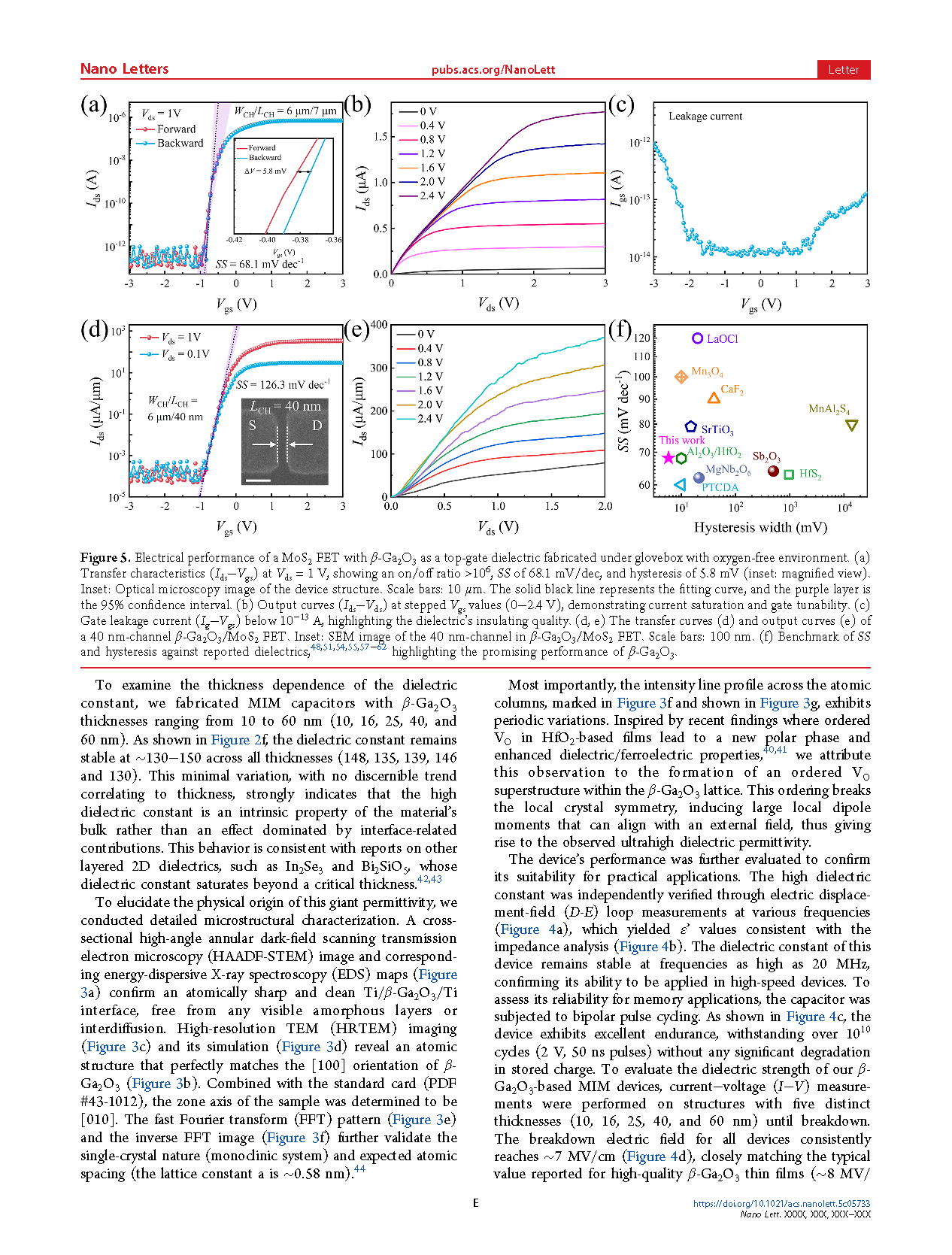
Figure 5. Electrical performance of a MoS2 FET with β-Ga2O3 as a top-gate dielectric fabricated under glovebox with oxygen-free environment. (a) Transfer characteristics (Ids−Vgs) at Vds = 1 V, showing an on/off ratio >106 , SS of 68.1 mV/dec, and hysteresis of 5.8 mV (inset: magnified view). Inset: Optical microscopy image of the device structure. Scale bars: 10 μm. The solid black line represents the fitting curve, and the purple layer is the 95% confidence interval. (b) Output curves (Ids−Vds) at stepped Vgs values (0−2.4 V), demonstrating current saturation and gate tunability. (c) Gate leakage current (Ig−Vgs) below 10−13 A, highlighting the dielectric’s insulating quality. (d, e) The transfer curves (d) and output curves (e) of a 40 nm-channel β-Ga2O3/MoS2 FET. Inset: SEM image of the 40 nm-channel in β-Ga2O3/MoS2 FET. Scale bars: 100 nm. (f) Benchmark of SS and hysteresis against reported dielectrics highlighting the promising performance of β-Ga2O3.
DOI:
doi.org/10.1021/acs.nanolett.5c05733