Paper Sharing
【Domestic Papers】Ultrahigh Responsivity β-Ga₂O₃ Solar-Blind Ultraviolet Photodetectors through In-situ Growth Pressure-Tuned Defect Engineering
日期:2026-02-26阅读:357
Researchers from the a Ningbo Institute of Materials Technology and Engineering, Chinese Academy of Sciences have published a dissertation titled "Ultrahigh Responsivity β-Ga2O3 Solar-Blind Ultraviolet Photodetectors through In-situ Growth Pressure-Tuned Defect Engineering" in Materials Today Physics.
Project Support
This work was supported by the National Natural Science Foundation of China (Grant No. 62304227), the Zhejiang Provincial Natural Science Foundation of China (Grant No. LQ23F040005), and the Ningbo Yongjiang Talent Introduction Program (Grant No. 2021A-046-C).
Background
Solar-blind ultraviolet (UV) photodetectors, which are intrinsically insensitive to solar background radiation, play a crucial role in a wide range of applications such as flame detection, secure communication, environmental monitoring, and missile warning systems. To meet the stringent requirements of these applications, extensive efforts have been devoted to the development of solar-blind UV photodetectors based on ultrawide-bandgap semiconductors, including AlGaN, ZnMgO, ZnGa₂O₄, diamond, and β-Ga₂O₃. Among these candidates, β-Ga₂O₃ has attracted particular attention owing to its ultrawide bandgap of 4.5–4.9 eV, high breakdown electric field, and excellent chemical and thermal stability. Despite these intrinsic advantages and the substantial progress achieved in recent years, the performance of β-Ga₂O₃-based photodetectors remains constrained by several critical issues, such as relatively high dark current, limited responsivity, and slow temporal response. These limitations are widely attributed to the presence of native point defects in β-Ga₂O₃, including oxygen vacancies, gallium vacancies, and gallium–oxygen divacancy complexes. Such defects can act as carrier trapping and recombination centers and are closely associated with persistent photoconductivity, thereby exerting a profound influence on the optoelectronic behavior of β-Ga₂O₃ photodetectors. To mitigate defect-related performance degradation, various post-growth approaches, including thermal annealing and surface passivation, have been explored. However, these strategies often offer limited controllability and do not fundamentally address defect formation during film growth. In contrast, in-situ defect engineering during epitaxial growth provides a more direct and systematic route for tailoring the defect landscape and, consequently, the electronic and optoelectronic properties of β-Ga₂O₃. Metal-organic chemical vapor deposition (MOCVD), with its precise control over growth parameters, represents a particularly powerful platform for this purpose.Among the key MOCVD growth parameters, deposition pressure plays a critical role in governing precursor transport, nucleation behavior, and adatom surface migration, all of which directly impact the incorporation of point defects. Nevertheless, a comprehensive understanding of how growth pressure influences defect evolution and photoresponse characteristics in β-Ga₂O₃ remains lacking. Addressing this gap is essential for establishing rational defect-engineering strategies toward high-performance solar-blind UV photodetectors.
Abstract
β-Ga2O3 is a promising material for solar-blind ultraviolet (UV) photodetectors, yet its performance is often limited by native point defects. Here, we demonstrate ultrahigh performance β-Ga2O3 photodetectors through in-situ defect engineering via growth-pressure modulation during metal-organic chemical vapor deposition. Systematic variation of deposition pressure from 40 to 100 mbar reveals a nonmonotonic formation of gallium-oxygen divacancy (VGa–VO) complexes governed by competing effects of precursor transport, surface nucleation, and adatom migration kinetics. X-ray photoelectron spectroscopy and photoluminescence analyses confirm that an intermediate pressure of 80 mbar maximizes VGa–VO defect incorporation by balancing adatom mobility and precursor kinetics. The VGa–VO complexes act as deep-level hole traps, prolonging carrier lifetimes and generating strong photoconductive gain. The β-Ga2O3 photodetector grown at 80 mbar exhibits an ultrahigh responsivity of 1.40 × 10⁴ A/W, a photo-to-dark current ratio of 1.88 × 10⁷, a detectivity of 1.12 × 10¹⁴ Jones, and rapid rise/decay times of 33.9/10.5 ms. This study establishes growth pressure-tuned defect engineering as an effective strategy for tailoring the optoelectronic properties of β-Ga2O3, providing a viable pathway toward high-performance solar-blind UV photodetectors.
Conclusion
We have demonstrated ultrahigh responsivity β-Ga₂O₃ photodetectors by employing in-situ defect control through growth-pressure modulation during MOCVD. Growth pressure-induced variations in surface nucleation, adatom mobility, and gas-phase reaction kinetics lead to a nonmonotonic formation of VGa–VO complexes, which function as deep-level centers that prolong carrier lifetimes and generate photoconductive gain. The β-Ga₂O₃ photodetector grown at 80 mbar exhibits outstanding performance, including a photo-to-dark current ratio of 1.88 × 10⁷, an ultrahigh responsivity of 1.4 × 10⁴ A/W, a detectivity of 1.12 × 10¹⁴ Jones, and fast rise/decay times of 33.9/10.5 ms. This study establishes a robust framework for tailoring the optoelectronic properties of β-Ga₂O₃ through in-situ defect engineering, providing valuable insights for the design and fabrication of next-generation high-performance solar-blind UV photodetectors.
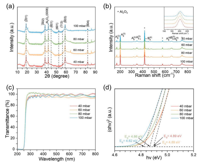
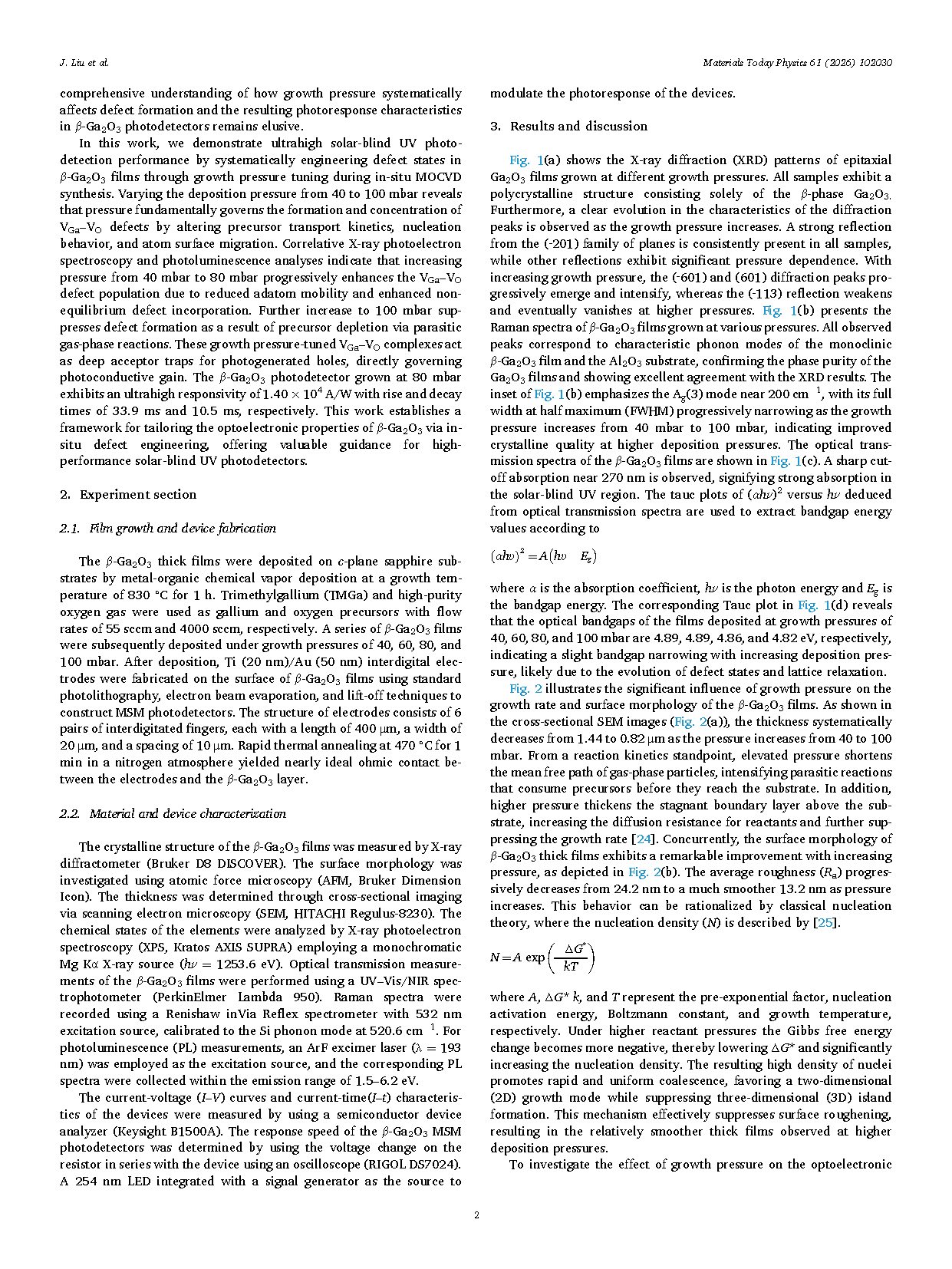
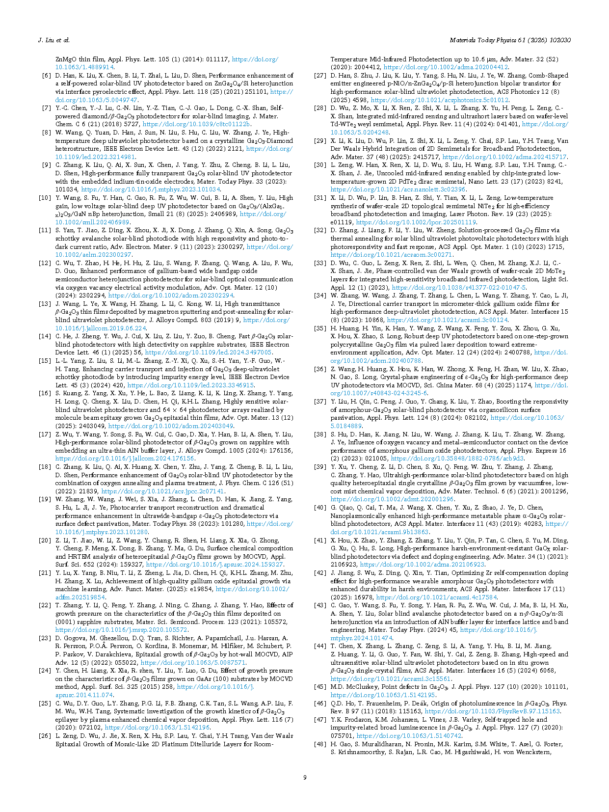
Fig. 1. (a) XRD patterns of the β-Ga₂O₃ films grown on the sapphire substrates with different growth pressures. (b) Raman spectra of the β-Ga₂O₃ films prepared at various growth pressures, and the inset displays the fitting results of the β-Ga₂O₃ Raman-active peak at 200 cm⁻¹. (c) Optical transmission spectra of the β-Ga₂O₃ films. (d) Tauc plots of the β-Ga₂O₃ films for the optical bandgap calculation.
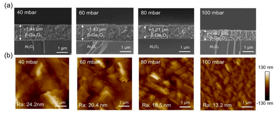
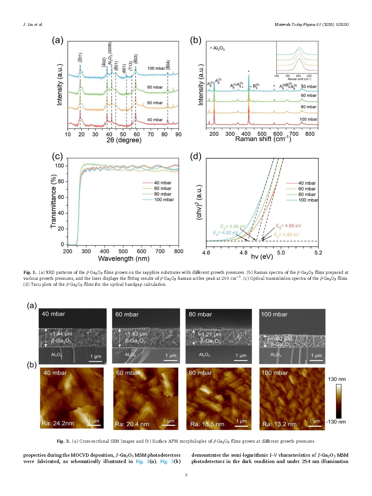
Fig. 2. (a) Cross-sectional SEM images and (b) Surface AFM morphologies of β-Ga2O3 films grown at different growth pressures.
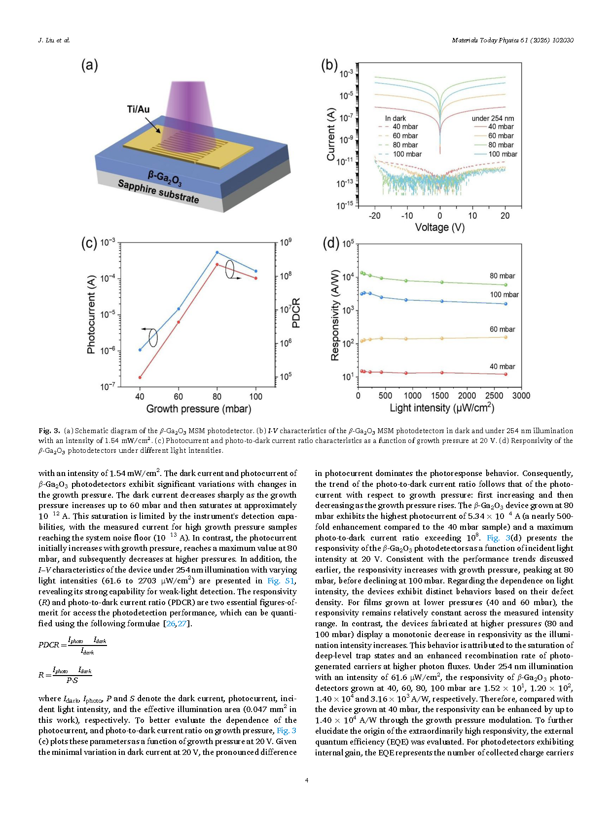
Fig. 3. (a) Schematic diagram of the β-Ga₂O₃ MSM photodetector. (b) I–V characteristics of the β-Ga₂O₃ MSM photodetectors in dark and under 254 nm illumination with an intensity of 1.54 mW/cm². (c) Photocurrent and photo-to-dark current ratio characteristics as a function of growth pressure at 20 V. (d) Responsivity of the β-Ga₂O₃ photodetectors under different light intensities.
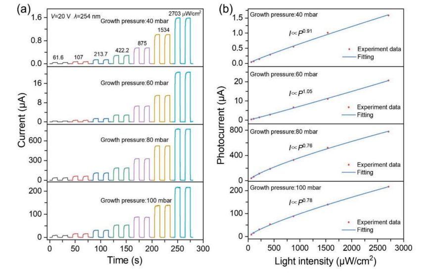
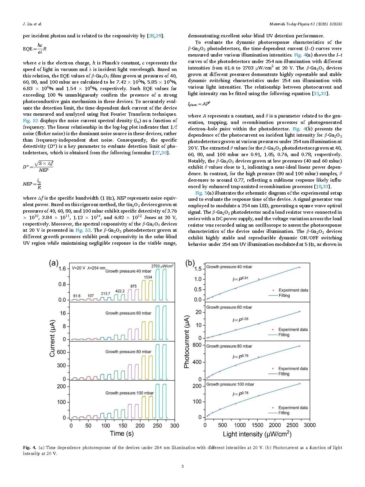
Fig. 4. (a) Time dependence photoresponse of the devices under 254 nm illumination with different intensities at 20 V. (b) Photocurrent as a function of light intensity at 20 V.
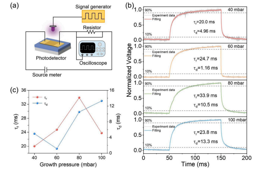
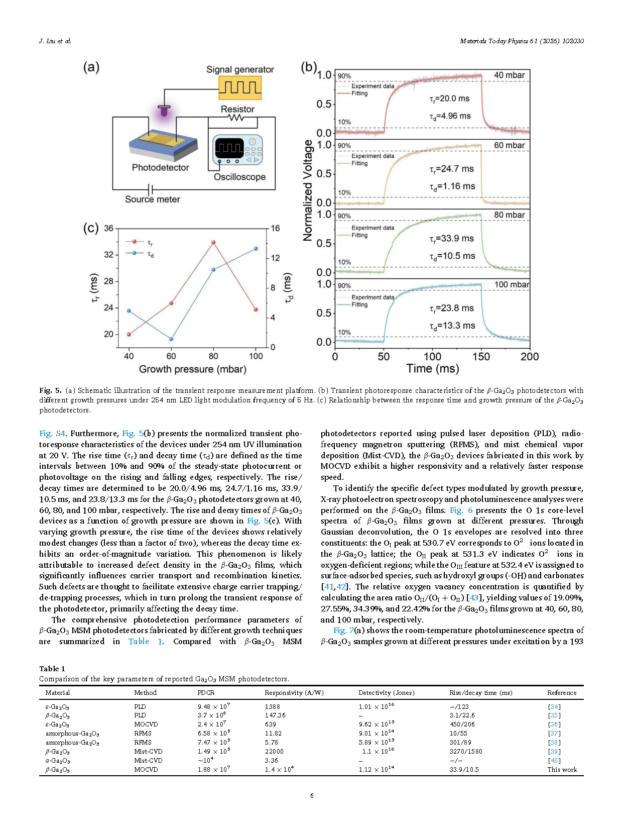
Fig. 5. (a) Schematic illustration of the transient response measurement platform. (b) Transient photoresponse characteristics of the β-Ga₂O₃ photodetectors with different growth pressures under 254 nm LED light modulation at a frequency of 5 Hz. (c) Relationship between the response time and growth pressure of the β-Ga₂O₃ photodetectors.
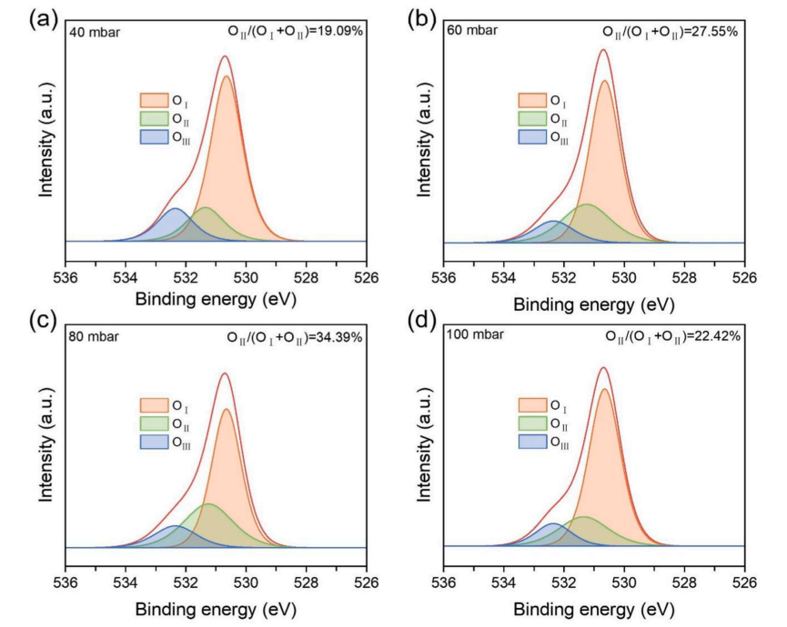
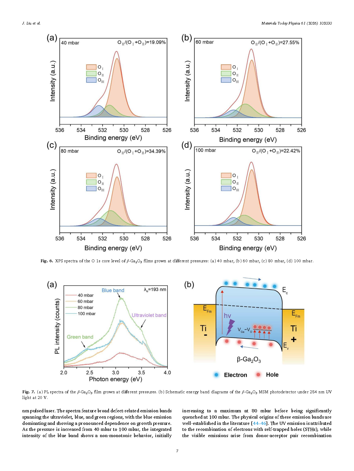
Fig. 6. XPS spectra of the O 1s core level of β-Ga₂O₃ films grown at different pressures: (a) 40 mbar, (b) 60 mbar, (c) 80 mbar, (d) 100 mbar.
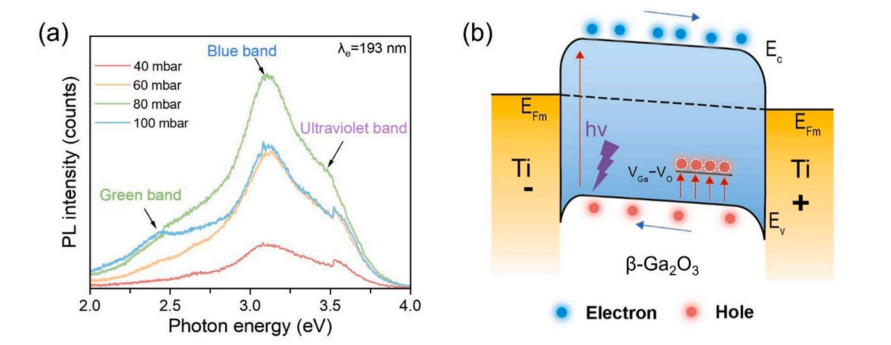
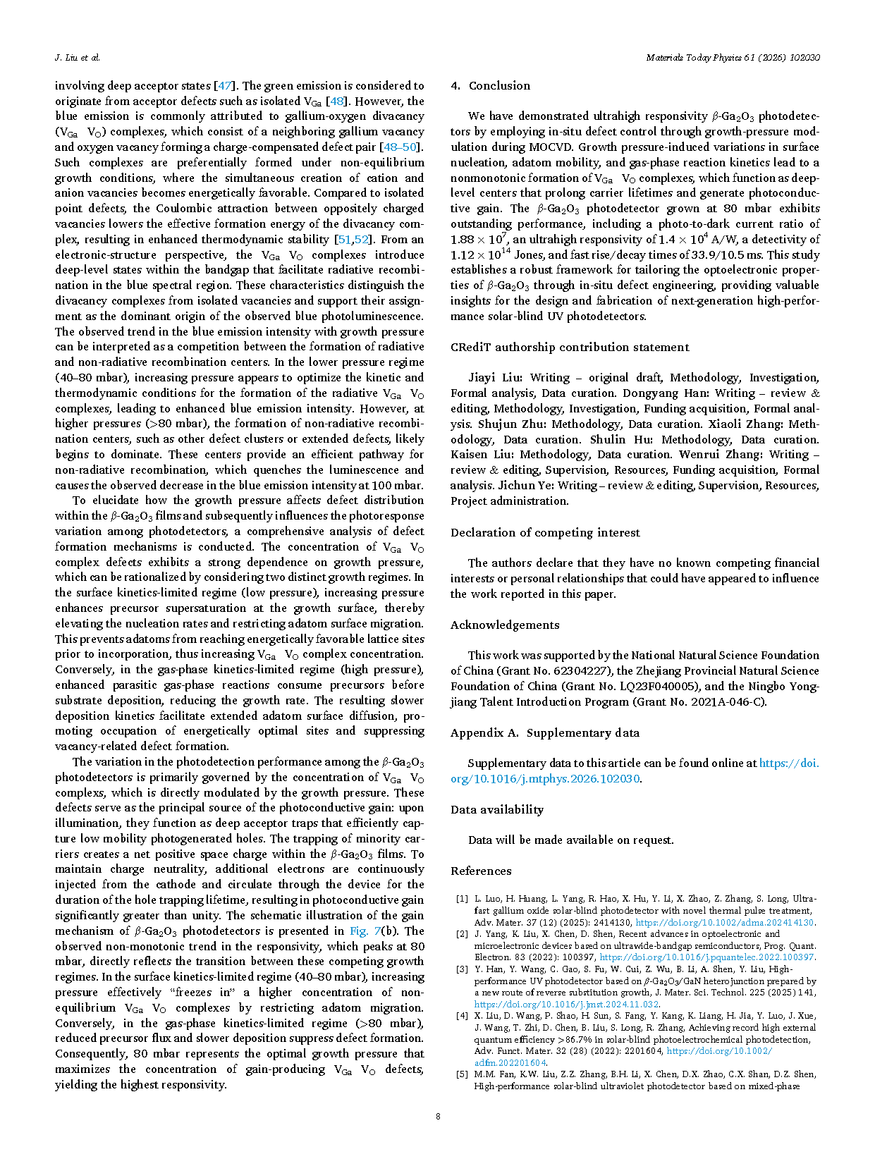
Fig. 7. (a) PL spectra of the β-Ga₂O₃ films grown at different pressures. (b) Schematic energy band diagrams of the β-Ga₂O₃ MSM photodetector under 254 nm UV light at 20 V.
DOI:
doi.org/10.1016/j.mtphys.2026.102030