Paper Sharing
【Member Papers】Deciphering the mechanism of enhanced scintillation properties in In-doped β-Ga₂O₃ ultrafast scintillation crystal
日期:2026-02-27阅读:347
Researchers from the Tongji University have published a dissertation titled "Deciphering the mechanism of enhanced scintillation properties in In-doped β-Ga2O3 ultrafast scintillation crystal" in Optics Express.
Background
β-Ga2O3, an ultra-wide bandgap semiconductor (4.7–4.9 eV), offers a high critical electric field (∼8 MV/cm) and excellent stability, making it promising for high-power electronics making it promising for high-power electronics, deep ultraviolet detection, and solar-blind detection applications. Beyond electronic and optoelectronic devices, β-Ga2O3 is also a luminescent material. Luminescence refers to non-thermal light emission arising from radiative electronic transitions following excitation by an external energy source. When the excitation is provided by high-energy ionizing radiation, this light-emission process is referred to as scintillation, which represents a specific form of luminescence and is directly relevant to radiation detection applications. Recently, β-Ga2O3 has also emerged as a fast-decay scintillator with unique advantages for medical imaging, space detection, and particle identification. These include an ultrafast decay time (<10 ns), high theoretical light yield (∼40800 ph/MeV), strong radiation resistance, and feasibility of large-scale single-crystal growth by melt techniques. Although β-Ga2O3 shows great potential as a scintillator, its application in radiation detection is limited by slow decay components (hundreds of ns) and sub-theoretical light yield. Doping can tune its electronic structure and recombination dynamics, offering a route to improved performance. However, most dopants show trade-offs: Si4+ shortens decay but reduces light yield, whereas Al3+ and Cu2+ increase light output but slow the decay. These contrasting effects highlight the need for advanced doping strategies to achieve balanced scintillation properties in β-Ga2O3 crystals.
Abstract
β-Ga2O3 is a promising ultrafast semiconductor scintillator, but its efficiency is hindered by low light yield and slow decay components. Here, high-quality β-Ga2O3:In single crystals were grown by the optical floating-zone method. In3+ incorporation narrows the bandgap (4.76 eV to 4.72 eV), redshifts photoluminescence, strengthens electron–phonon coupling, and accelerates recombination, with a 91 meV activation energy for blue-to-ultraviolet energy transfer. Compared to unintentionally doped (UID) β-Ga2O3, the β-Ga2O3:In bulk single crystal demonstrates enhanced light yields of (3348 ± 310) ph/MeV and (5664 ± 710) ph/5.5 MeV under 662 keV γ-ray and 5.5 MeV α-ray excitation, respectively, using Bi4Ge3O12 (BGO) as the reference scintillator, together with a markedly faster nanosecond-scale decay. The improved performance is attributed to enhanced charge transport and carrier recombination, highlighting its potential for ultrafast radiation detection.
Conclusion
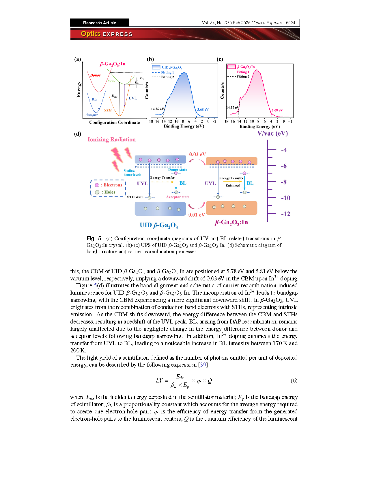
In summary, high-quality β-Ga2O3:In bulk single crystals were successfully synthesized, and their luminescence and scintillation properties systematically investigated. About 1 at% In3+ doping reduces the bandgap by 0.04 eV. UVL and BL exhibit distinct electron–phonon coupling with effective phonon energies of 38 and 44 meV, respectively, and enhanced UVL-to-BL energy transfer (Ea2 = 91 meV) leads to anomalous thermal BL enhancement. In3+ doping also leads to enhanced scintillation performance. Under 662 keV γ-ray excitation, using a commercial BGO scintillator as the reference, the light yield increases from (2797 ± 270) to (3348 ± 310) ph/MeV, while the fast component (∼4 ns) is preserved and the slow component is shortened from 331.3 ns (84.3%) to 148.5 ns (73.0%). Under 5.5 MeV α-ray excitation, β-Ga2O3:In exhibits a higher light yield (5664 ± 710 ph/5.5 MeV) compared with the UID β-Ga2O3 (5428 ± 650 ph/5.5 MeV), together with an increased fast-component fraction and a reduced contribution from the slow component. A comprehensive model incorporating band structure changes and carrier pathways explains the enhanced light yield and accelerated decay. This study provides fundamental insights into β-Ga2O3:In luminescence and highlights its potential for ultrafast scintillators and advanced optoelectronic applications.
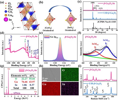
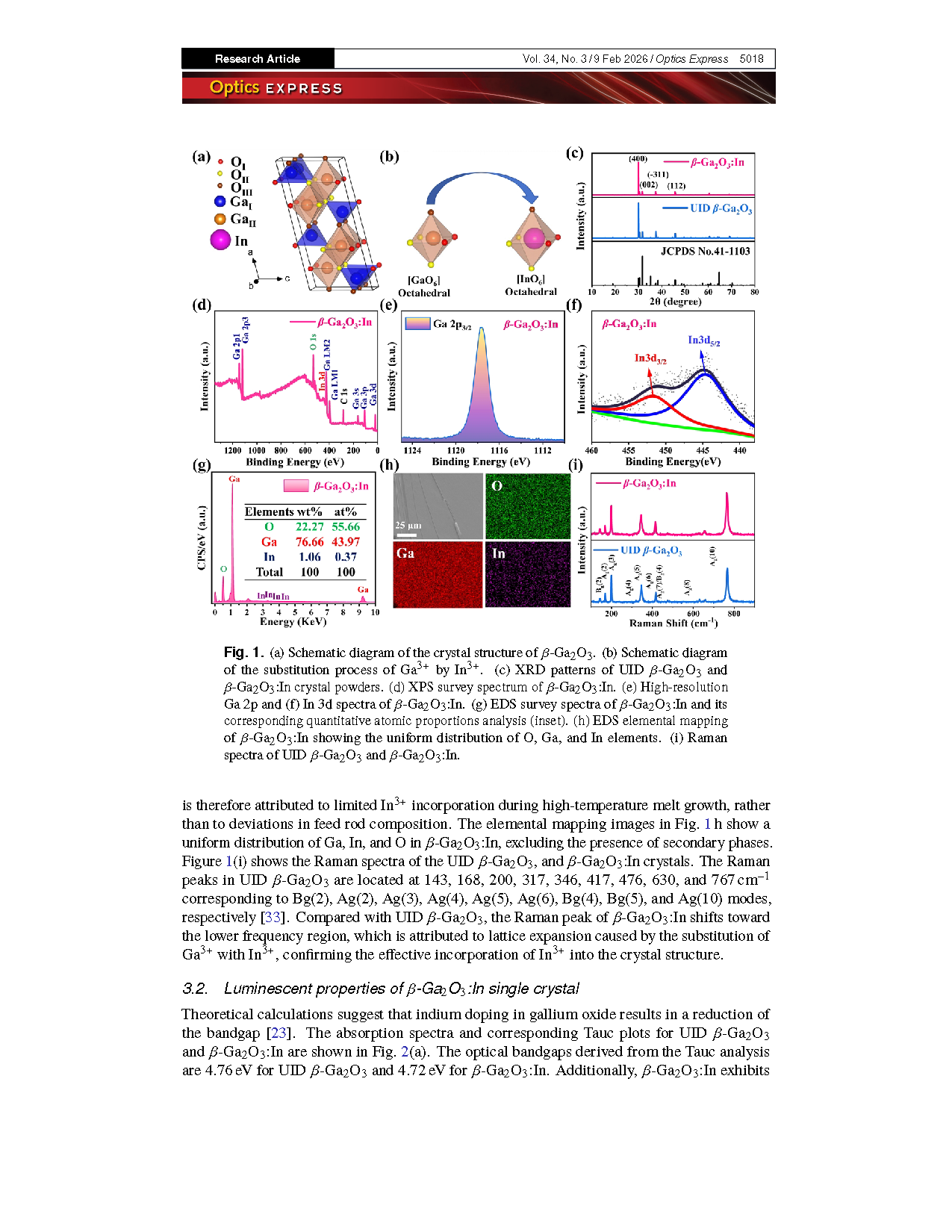
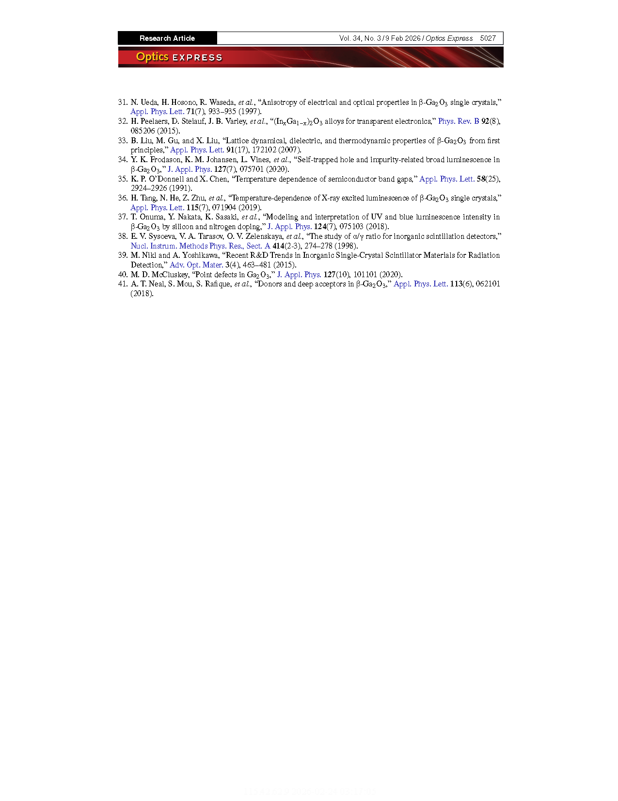
Fig. 1. (a) Schematic diagram of the crystal structure of β-Ga2O3. (b) Schematic diagram of the substitution process of Ga3+ by In3+. (c) XRD patterns of UID β-Ga2O3 and β-Ga2O3:In crystal powders. (d) XPS survey spectrum of β-Ga2O3:In. (e) High-resolution Ga 2p and (f) In 3d spectra of β-Ga2O3:In. (g) EDS survey spectra of β-Ga2O3:In and its corresponding quantitative atomic proportions analysis (inset). (h) EDS elemental mapping of β-Ga2O3:In showing the uniform distribution of O, Ga, and In elements. (i) Raman spectra of UID β-Ga2O3 and β-Ga2O3:In.
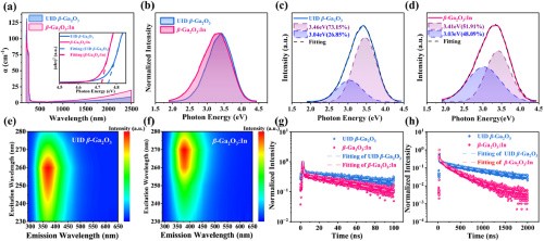
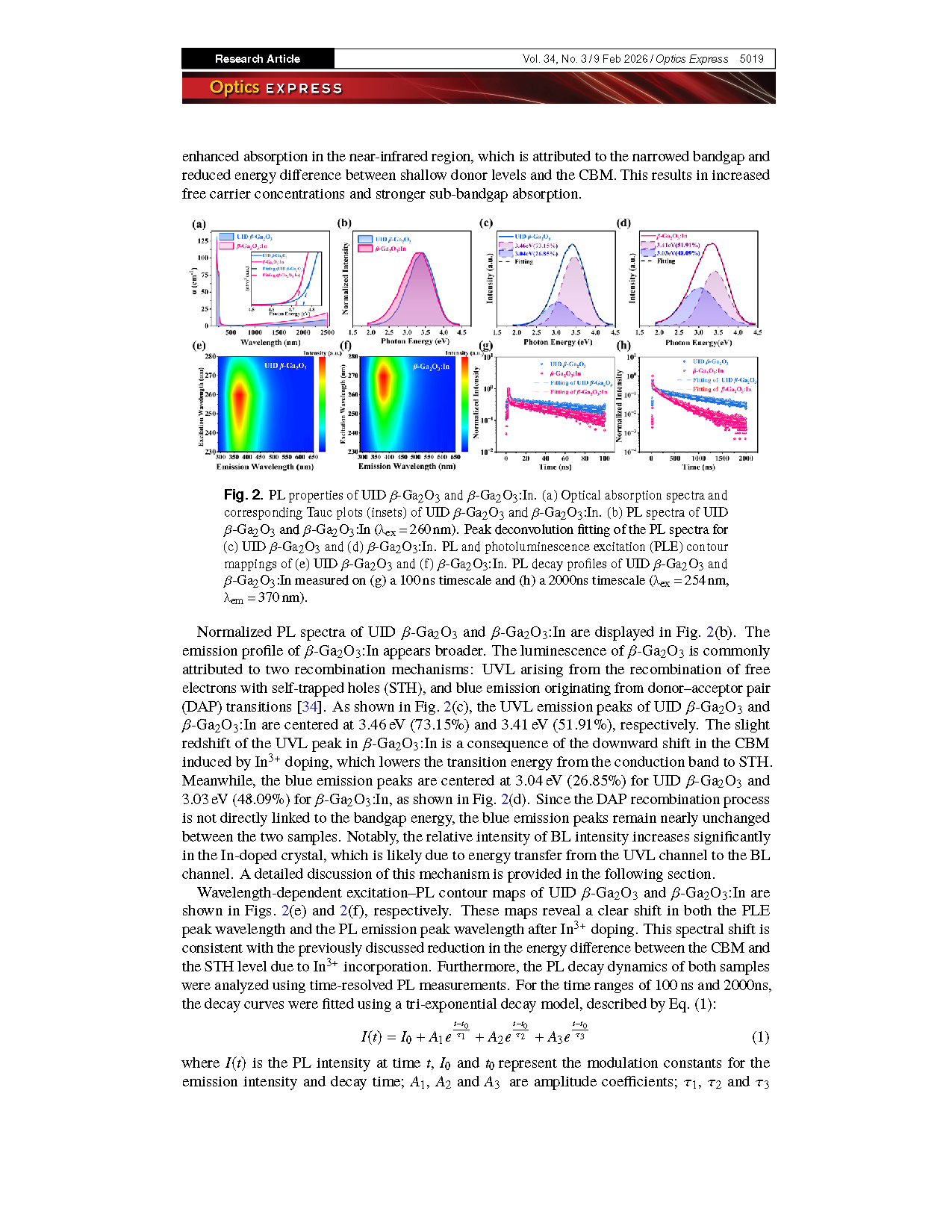
Fig. 2. PL properties of UID β-Ga2O3 and β-Ga2O3:In. (a) Optical absorption spectra and corresponding Tauc plots (insets) of UID β-Ga2O3 and β-Ga2O3:In. (b) PL spectra of UID β-Ga2O3 and β-Ga2O3:In (λex = 260 nm). Peak deconvolution fitting of the PL spectra for (c) UID β-Ga2O3 and (d) β-Ga2O3:In. PL and photoluminescence excitation (PLE) contour mappings of (e) UID β-Ga2O3 and (f) β-Ga2O3:In. PL decay profiles of UID β-Ga2O3 and β-Ga2O3:In measured on (g) a 100 ns timescale and (h) a 2000ns timescale (λex = 254 nm, λem = 370 nm).
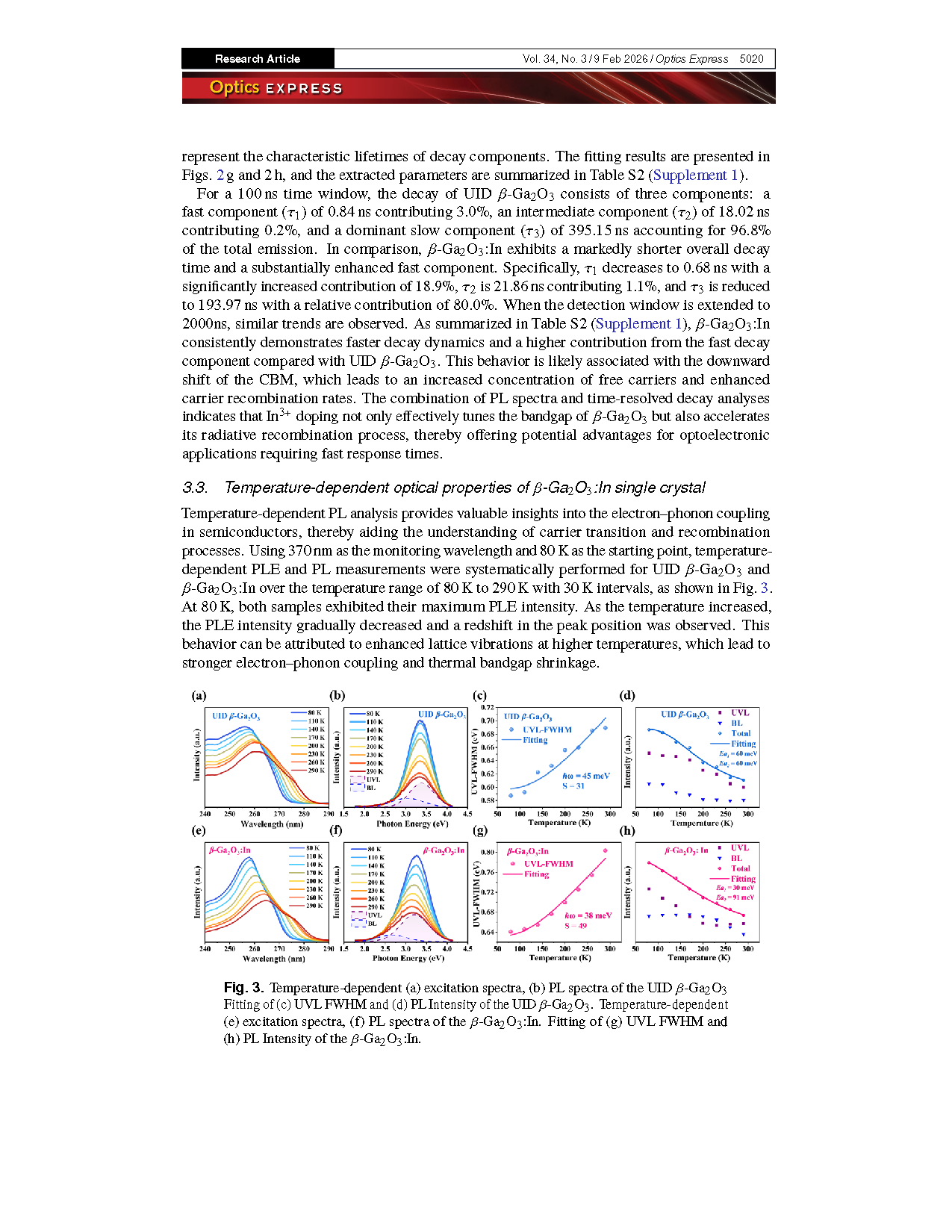
Fig. 3. Temperature-dependent (a) excitation spectra, (b) PL spectra of the UID β-Ga2O3 Fitting of (c) UVL FWHM and (d) PL Intensity of the UID β-Ga2O3. Temperature-dependent (e) excitation spectra, (f) PL spectra of the β-Ga2O3:In. Fitting of (g) UVL FWHM and (h) PL Intensity of the β-Ga2O3:In.
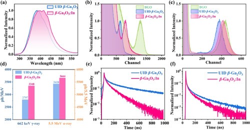
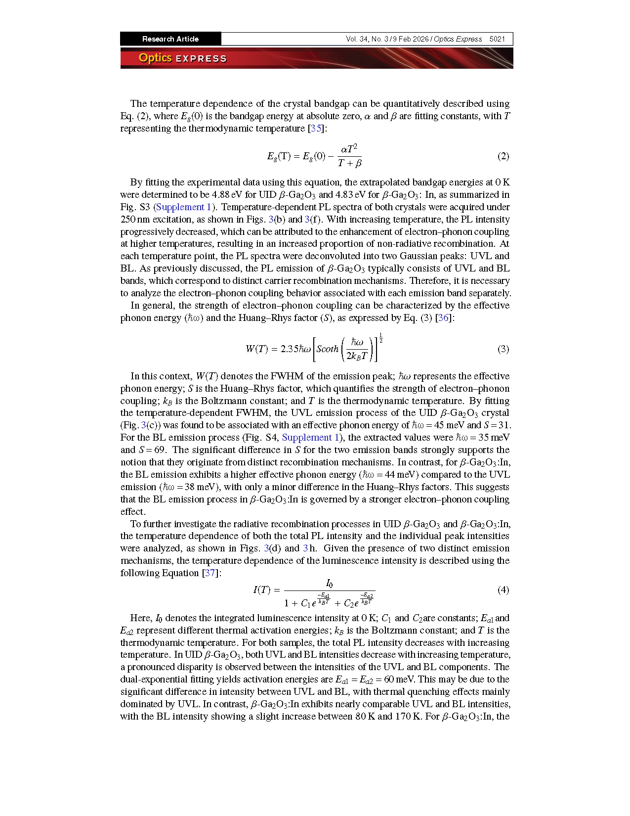
Fig. 4. (a) Radiation luminescence spectra of UID β-Ga2O3 and β-Ga2O3:In crystals under X-ray excitation. (b)-(c) Pulse-height spectra of UID β-Ga2O3 and β-Ga2O3:In single crystals under excitation by 662 keV γ-ray from a 137Cs source and 5.5 MeV α-ray from a 241Am source, respectively, with a commercial BGO scintillator used as the reference. (d) Scintillation light yields of UID β-Ga2O3 and β-Ga2O3:In under 662 keV γ-ray and 5.5 MeV α-ray excitation, determined relative to the BGO reference after correction for the PMT spectral response. Numerical labels indicate the mean light-yield values; corresponding uncertainties (1σ) are provided in the text. (e)-(f) Scintillation decay curves of UID β-Ga2O3 and β-Ga2O3:In under excitation by 662 keV γ-ray and 5.5 MeV α-ray, respectively.
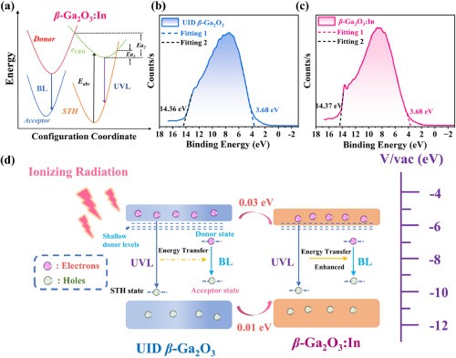
Fig. 5. (a) Configuration coordinate diagrams of UV and BL-related transitions in β-Ga2O3:In crystal. (b)-(c) UPS of UID β-Ga2O3 and β-Ga2O3:In. (d) Schematic diagram of band structure and carrier recombination processes.
DOI:
doi.org/10.1364/OE.584439