Paper Sharing
【Member Papers】Theoretical insights into β-Ga₂O₃/diamond heterojunction interfaces: Surface selection, band alignment, and interfacial interaction
日期:2026-03-05阅读:413
Researchers from Wuhan University have published a paper titled “Theoretical Insights into β-Ga₂O₃/Diamond Heterojunction Interfaces: Surface Selection, Band Alignment, and Interfacial Interaction” in Applied Physics Letters. The study was authored by doctoral student Feng Jiaren as the first author, with Professor Zhang Zhaofu from the team of Academician Liu Sheng at the School of Integrated Circuits, Wuhan University, serving as the corresponding author.
Background
β-Ga₂O₃, with its ultra-wide bandgap (~4.85 eV), high critical breakdown field, and outstanding Baliga’s figure of merit (~3444), has emerged as a key material for electronic and optoelectronic applications. However, its relatively low thermal conductivity and the difficulty of achieving p-type doping limit further device development. Heterogeneous integration of β-Ga₂O₃ with diamond—a high-thermal-conductivity p-type wide-bandgap semiconductor—offers an effective strategy to overcome these bottlenecks. As a result, β-Ga₂O₃/diamond heterojunctions show great promise for both power and optoelectronic devices.
Band alignment is a critical factor determining heterojunction performance. Existing experimental studies have reported significantly different valence band offsets (1.12–2.9 eV), largely due to variations in surface orientation, interface termination, and measurement methods. While theoretical studies can provide more precise values for valence band offsets, research on β-Ga₂O₃/diamond interfaces remains limited because of the complexity of interface modeling and bonding configurations.
Main Content
In this study, density functional theory (DFT) was employed to systematically investigate β-Ga₂O₃/diamond heterojunctions based on crystal-plane combinations previously reported in experiments. All constructed interface models—both covalently bonded and hydrogen-terminated—satisfy the electron counting rule and exhibit negative formation energies.
The calculations reveal that all heterojunctions display type-II band alignment. For covalently bonded interfaces, the valence band offset ranges from 1.84 eV to 2.78 eV and is modulated by material anisotropy and lattice-mismatch-induced strain, confirming the effectiveness of surface selection for tuning interfacial barriers. Hydrogen termination can further increase the valence band offset by 1.11–1.88 eV, reaching a maximum value of 3.89 eV.
Interfacial charge transfer analysis shows that electrons transfer from the diamond side to the β-Ga₂O₃ side, with the transfer pattern governed by atomic electronegativity differences. At covalently bonded interfaces, band bending occurs near the interface—an upward bending of the β-Ga₂O₃ valence band maximum and a downward bending of the diamond conduction band minimum—which effectively lowers the actual interface barrier and facilitates carrier transport.
However, hydrogen termination introduces a van der Waals gap at the interface. The resulting vacuum-like barrier layer significantly hinders intrinsic carrier transport and prevents complete Fermi-level alignment across the interface, leading to the formation of a built-in electric field within the depletion region.
Conclusion
This theoretical study systematically reveals the interfacial properties of β-Ga₂O₃/diamond heterojunctions under different surface orientations and termination conditions. The results show that selecting different crystal-plane combinations can dynamically tune the valence band offset by nearly 1 eV, while hydrogen termination can further increase the offset by 1.11–1.88 eV.
Covalently bonded interfaces, with moderate valence band offsets and favorable band bending that facilitates carrier transport, are more suitable for applications such as photodetectors. In contrast, hydrogen-terminated interfaces—although unfavorable for photogenerated carrier collection due to their large valence band offset and van der Waals barrier—exhibit strong carrier blocking capability and effective interface passivation. This makes them promising for applications requiring leakage current suppression, such as serving as β-Ga₂O₃ epitaxial substrates.
Overall, this work provides an important theoretical foundation for the design and performance optimization of β-Ga₂O₃/diamond heterojunction devices.

Figure 1 Atomic structure relaxation diagrams of the Gallium Oxide/diamond interfaces with different crystal planes and terminations.

Figure 2 (a) Differential charge density of β-Ga₂O₃(−201)/diamond(100); (b) differential charge density of β-Ga₂O₃(−201)/H-terminated diamond(100); (c) electrostatic potential distribution of β-Ga₂O₃(−201)/diamond(100); (d) electrostatic potential distribution of β-Ga₂O₃(−201)/H-terminated diamond(100).

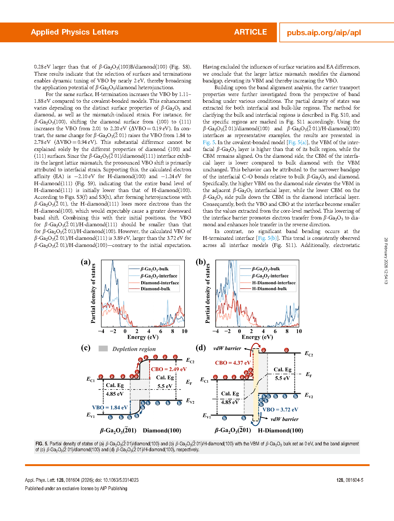
Figure 3 Band alignment diagrams of β-Ga₂O₃/diamond interfaces with different surface orientations and terminations. For consistent comparison, the valence band maximum of β-Ga₂O₃ is set to 0 eV.

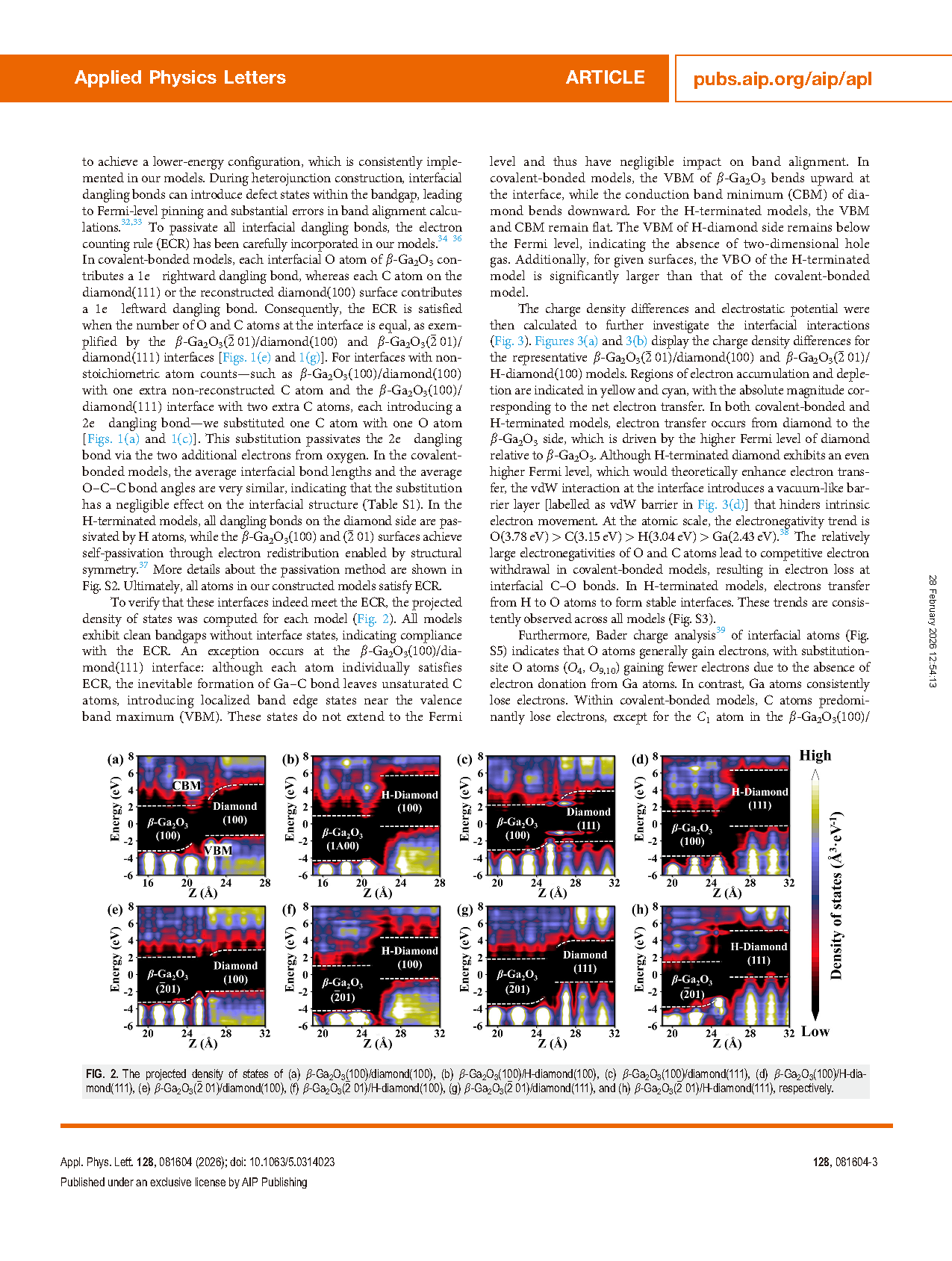
Figure 4 (a) Projected density of states (PDOS) of the β-Ga₂O₃(−201)/diamond(100) interface; (b) PDOS of the β-Ga₂O₃(−201)/H-terminated diamond(100) interface; (c) schematic band alignment of β-Ga₂O₃(−201)/diamond(100); (d) schematic band alignment of β-Ga₂O₃(−201)/H-terminated diamond(100).
DOI:
10.1063/5.0314023