


Member News
【Member News】First Attempt at Full Industry Chain Integration: Fujia Gallium’s High-Quality Epitaxial Wafers Enable Deep Advancement of the Ga₂O₃ “Materials–Devices–Applications” Chain
日期:2026-03-16阅读:376
Hangzhou Fujia Gallium Technology Co., Ltd. (hereinafter referred to as “Fujia Gallium”) has partnered with Shanghai CoolSemi Semiconductor Technology Co., Ltd. (hereinafter referred to as “CoolSemi”) to jointly tackle key technologies for the industrialization of the fourth-generation semiconductor Gallium Oxide (Ga₂O₃). The collaboration spans the entire value chain—from materials and devices to applications—and has now progressed to the device verification stage. According to reports, this marks China’s first attempt to establish a fully integrated Gallium Oxide industry chain.
In the recently released Outline of the 15th Five-Year Plan for National Economic and Social Development of the People’s Republic of China, China clearly proposed to “accelerate the upgrading of the wide-bandgap semiconductor industry and promote the industrialization of ultra-wide-bandgap semiconductors such as Gallium Oxide and diamond.” This joint initiative precisely targets key application demands in new energy storage and liquid-cooling systems for data centers, while also aligning with the product development requirements of CoolSemi’s 400 V motor drive platform, leading to multiple breakthroughs in key technologies.
Leveraging high-quality MOCVD-grown Gallium Oxide epitaxial wafers independently developed by Fujia Gallium and the fabrication of high-performance Gallium Oxide vertical schottky diode devices, CoolSemi has carried out device packaging and application verification. At present, the Gallium Oxide diode device has successfully passed chip-level testing and packaging processes, and CoolSemi is advancing its validation in liquid-cooling modules. These efforts will help establish a solid technological foundation for future large-scale commercialization, while also providing strong practical support for achieving independent and controllable core technologies in China’s fourth-generation semiconductor sector.
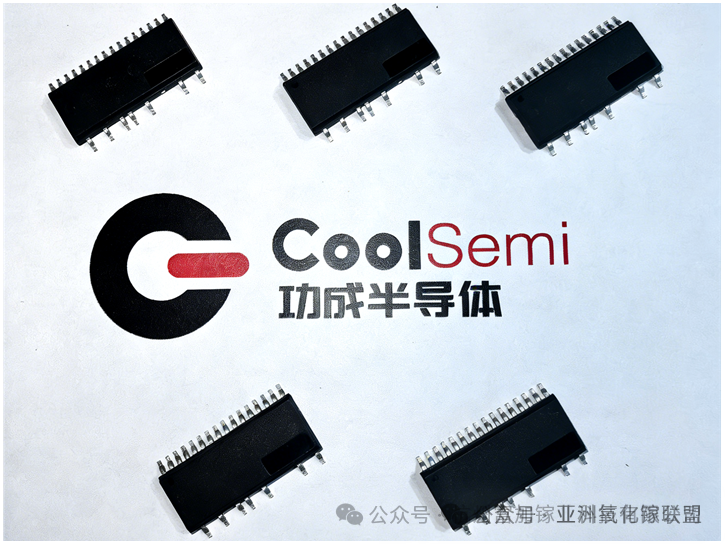
Packaged Ga₂O₃ SBD Device Based on Fujia Gallium’s MOCVD Epitaxial Wafers
Company Profile
Hangzhou Fujia Gallium Technology Co., Ltd. (hereinafter referred to as “Fujia Gallium”) was established on December 31, 2019, and focuses on the industrialization of ultra-wide-bandgap semiconductor Gallium Oxide (Ga₂O₃) materials. Its core products include Gallium Oxide single-crystal substrates, MOCVD/MBE epitaxial wafers, as well as crystal growth equipment based on the Vertical Bridgman (VB) method and Edge-defined Film-fed Growth (EFG) method, providing systematic solutions for both material development and large-scale production. With the vision of “enabling the world to use better materials,” the company is committed to accelerating the development of the entire Gallium Oxide industry chain and promoting the application of Gallium Oxide materials in fields such as power devices, microwave RF devices, and optoelectronic detection.
Fujia Gallium has been recognized as a National High-Tech Enterprise, a Zhejiang Province Technology-based SME, a Zhejiang Province “Specialized, Refined, Distinctive and Innovative” SME, the Hangzhou Enterprise High-Tech R&D Center, and a Hangzhou “Young Eagle” Enterprise, among other honors. In 2025, the company obtained ISO 9001 quality management system certification. It has undertaken multiple national and provincial-level research and industrialization projects funded by organizations including the National Development and Reform Commission (NDRC), the Ministry of Industry and Information Technology (MIIT), the National Natural Science Foundation of China (NSFC), as well as authorities in Zhejiang Province and Shanghai. A number of its key achievements have been featured by major media outlets such as CCTV-1, CCTV-2, People’s Daily, Xinhua Net, China Securities Journal, and The Paper.
The company currently holds 14 authorized international patents, 42 authorized domestic patents, and 5 software copyrights, including the “One-Click Crystal Growth” control software. It is also leading the drafting of the first national standard in the Gallium Oxide field.
Shanghai CoolSemi Semiconductor Technology Co., Ltd. was established in May 2018, with its headquarters in Shanghai and branch offices in Wuxi, Shenzhen, and Chengdu. Guided by market demand and driven by technological innovation, CoolSemi is dedicated to the research, development, and industrialization of semiconductor power devices, providing customers with efficient and reliable products. The company focuses on the design and development of low-voltage Shielded Gate Trench (SGT) MOSFETs, high-voltage Super Junction (SJ) devices, trench-gate field-stop IGBTs, SiC Schottky Barrier Diodes (SBDs), SiC MOSFETs, GaN HEMTs, power modules (IPM), and power ICs.
CoolSemi primarily targets application areas including new energy, data centers, automotive electronics, smart home appliances, and high-end consumer electronics. Its products have been widely adopted in segments such as DC charging stations, communication power supplies, server power supplies, portable energy storage systems, residential energy storage, photovoltaic inverters, and automotive PTC heaters.
With a diversified product portfolio, CoolSemi has successfully entered the supply chains of multiple well-known enterprises. The company maintains close collaboration with leading domestic wafer foundries and packaging/testing service providers, and operates a comprehensive ISO 9001 quality management system, ensuring consistent product quality and stable supply.
