Paper Sharing
【International Papers】Mitigating Plasma Etch-Induced Negative Charge Trapping in 2.7 kV β-Ga₂O₃ (001) Trench Schottky Barrier Diodes Using H₃PO₄ Treatment
日期:2026-03-17阅读:237
Researchers from the University of Bristol have published a dissertation titled "Mitigating Plasma Etch-Induced Negative Charge Trapping in 2.7 kV β-Ga2O3 (001) Trench Schottky Barrier Diodes Using H3PO4 Treatment" in ACS Applied Electronic Materials.
Background
Beta-gallium oxide (β-Ga2O3) has attracted considerable attention for its ability to enable compact and energy-efficient power electronic devices, addressing the increasing power requirements of transportation, computing, and data center applications. Its ultrawide bandgap (4.9 eV) results in a high critical electric field (8 MV cm–1) and an associated high Baliga’s figure-of-merit (BFOM). Furthermore, the availability of potentially low-cost single-crystal substrates has positive implications for commercial uptake in mass-market power electronics applications. Recent demonstrations in vertical unipolar Ga2O3 devices include vertical trench Schottky barrier diodes (TSBDs) of up to 4 kV and transistors reaching over 10 kV. Surface field engineering in TSBDs, i.e., reduced surface field (RESURF) designs, is essential to fully exploit the high critical field strength of Ga2O3. Due to the lack of p-type doping in Ga2O3, implementation of conventional RESURF structures though is limited. TSBDs employ trench structures that exploit sidewall metal-oxide-semiconductor (MOS) capacitance to redistribute electric fields, offering a RESURF-like benefit in device performance.
Abstract
Stable β-Ga2O3 (001) trench Schottky barrier diodes (TSBDs) with a Baliga’s figure-of-merit (BFOM) of 0.7 GW cm–2 were demonstrated by reducing the Al2O3/Ga2O3 interface state trap density using a H3PO4 surface treatment during device fabrication. TSBDs with fins oriented along different directions have been studied, wherein devices with [010] fin orientation exhibited a low specific on-resistance (Ron,sp) of 11 mΩ cm2 and a breakdown voltage (Vbr) of up to 2.7 kV with H3PO4 treatment. Reliability testing using sequential voltage stress up to a reverse bias of −1.2 kV showed a degradation in Ron,sp by 20% in untreated devices but only by 9% in those with the H3PO4 surface treatment. TCAD simulations confirm that the H3PO4 treatment mitigates the density of negative interface charges, highlighting the effectiveness of the acid treatment in controlling defect-mediated instabilities. Furthermore, high-temperature bias stress tests demonstrated that [010]-oriented TSBDs achieved superior thermal and electrical stability after the treatment, eliminating the 10% Ron,sp increase observed in untreated devices. These results establish H3PO4 surface treatment as an effective strategy for enhancing the robustness of β-Ga2O3 power devices under combined thermal and electrical stress.
Conclusion
We studied the effect of H3PO4 surface treatment on the electrical performance and reliability under high-temperature and bias stressing in β-Ga2O3 TSBDs using measurements and simulations. At RT, the treatment ensured stable operation for [140]- and [120]-oriented TSBDs, while the [010]-oriented TSBD achieves a notable performance increase, with Ron,sp reduced from 13 to 11 mΩ cm2 and Vbr increased from 2.5 to 2.7 kV, resulting in a BFOM of approximately 0.7 GW cm–2. Under sequential voltage stress at reverse bias of up to −1.2 kV, untreated devices exhibited a 26% increase in Ron,sp, compared to only 11% in H3PO4-treated devices, and only 1 h was required for near-complete recovery. Furthermore, high-temperature reliability was confirmed at 150 °C, where H3PO4-treated TSBDs retained stable performance across repeated measurements, in contrast to untreated devices that exhibited a 10% Ron,sp increase and a positive Von shift. Overall, these findings underscore the importance of controlling interface charges and surface defects through surface treatments during device processing for enabling robust and reliable β-Ga2O3 TSBD operation under combined electrical and thermal stress, paving the way for high-voltage power electronics in harsh environments.
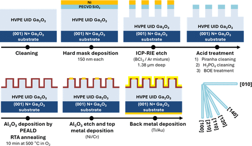
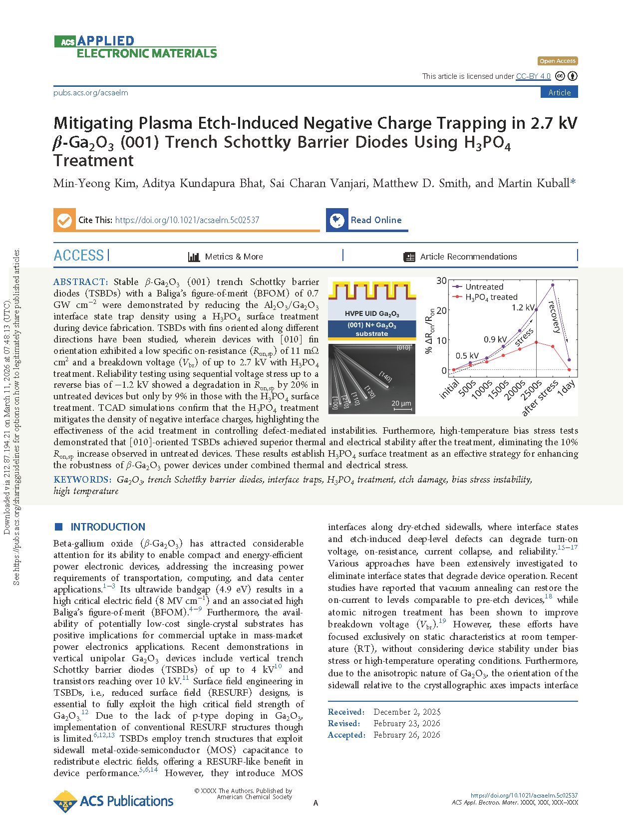
Figure 1. Schematics of the trench Schottky barrier diode (TSBD) with fabrication process flow and different fin orientations implemented in this study.
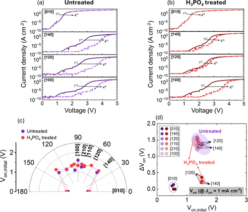
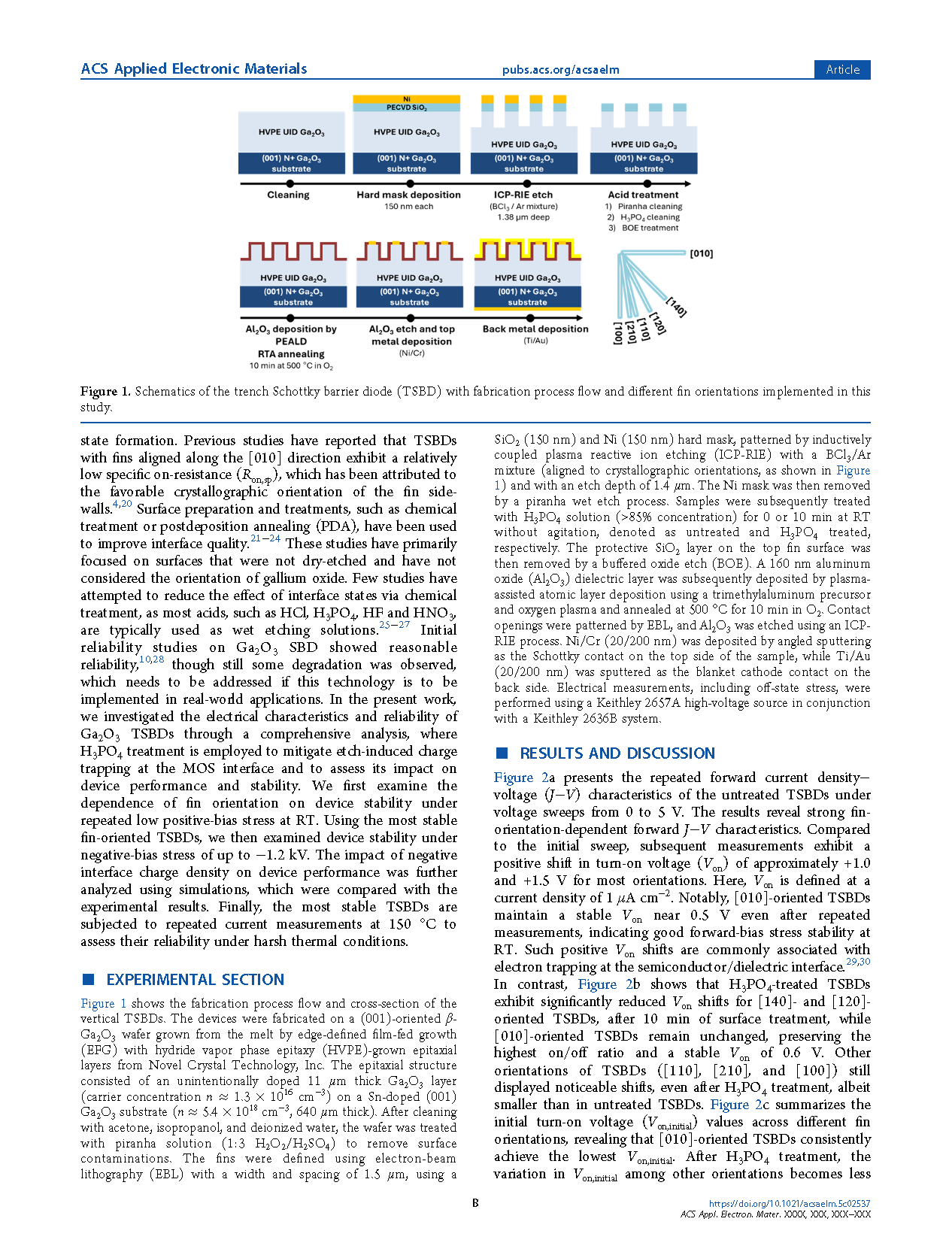
Figure 2. Repeated current density–voltage (J–V) characteristics from 0 to 5 V of Ga2O3 TSBDs with different fin orientations: (a) untreated and (b) H3PO4-treated TSBD. (c) Von,initial as a function of fin orientation, untreated and H3PO4 treated. (d) Summary plots of ΔVon vs Von,initial, measured at RT under repeated voltage sweeps from 0 to 5 V. ΔVon denotes the shift in Von between the fourth and the initial measurements.
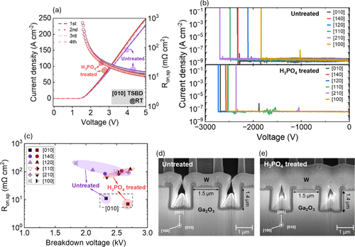
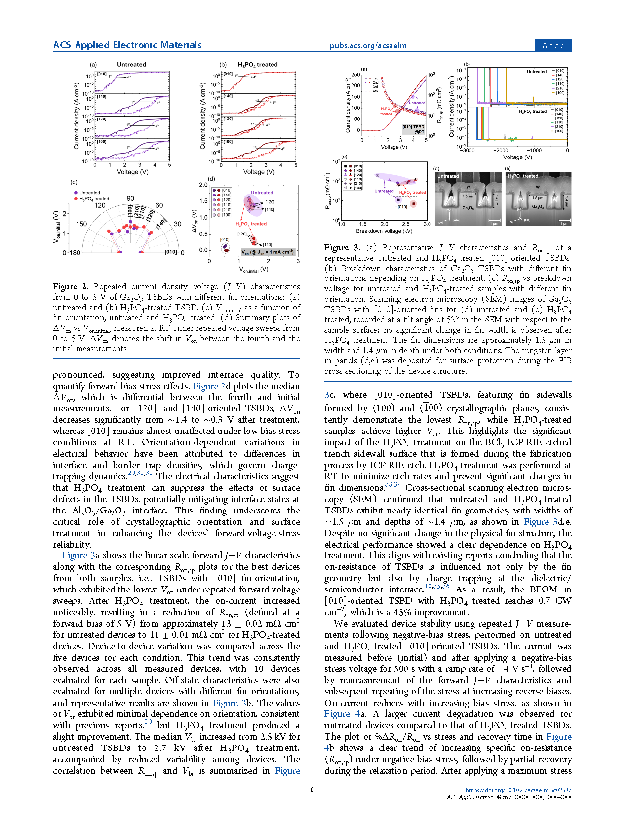
Figure 3. (a) Representative J–V characteristics and Ron,sp of a representative untreated and H3PO4-treated [010]-oriented TSBDs. (b) Breakdown characteristics of Ga2O3 TSBDs with different fin orientations depending on H3PO4 treatment. (c) Ron,sp vs breakdown voltage for untreated and H3PO4-treated samples with different fin orientation. Scanning electron microscopy (SEM) images of Ga2O3 TSBDs with [010]-oriented fins for (d) untreated and (e) H3PO4 treated, recorded at a tilt angle of 52° in the SEM with respect to the sample surface; no significant change in fin width is observed after H3PO4 treatment. The fin dimensions are approximately 1.5 μm in width and 1.4 μm in depth under both conditions. The tungsten layer in panels (d,e) was deposited for surface protection during the FIB cross-sectioning of the device structure.
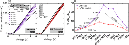
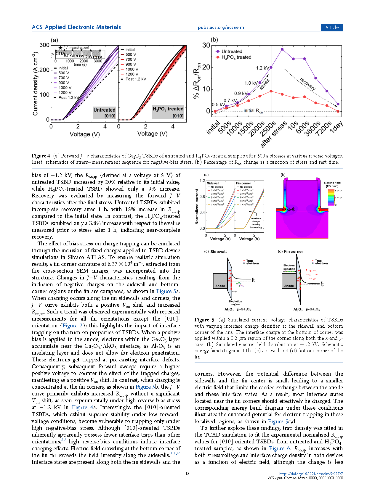
Figure 4. (a) Forward J–V characteristics of Ga2O3 TSBDs of untreated and H3PO4-treated samples after 500 s stresses at various reverse voltages. Inset: schematics of stress–measurement sequence for negative-bias stress. (b) Percentage of Ron change as a function of stress and rest time.
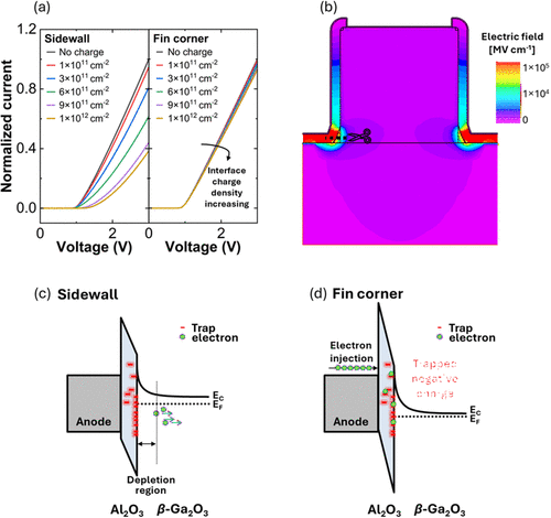
Figure 5. (a) Simulated current–voltage characteristics of TSBDs with varying interface charge densities at the sidewall and bottom corner of the fins. The interface charge at the bottom of corner was applied within a 0.2 μm region of the corner along both the x-and y-axes. (b) Simulated electric field distribution at −1.2 kV. Schematic energy band diagram at the (c) sidewall and (d) bottom corner of the fin.
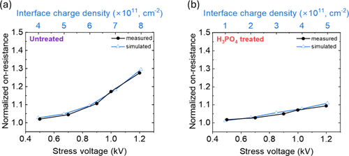
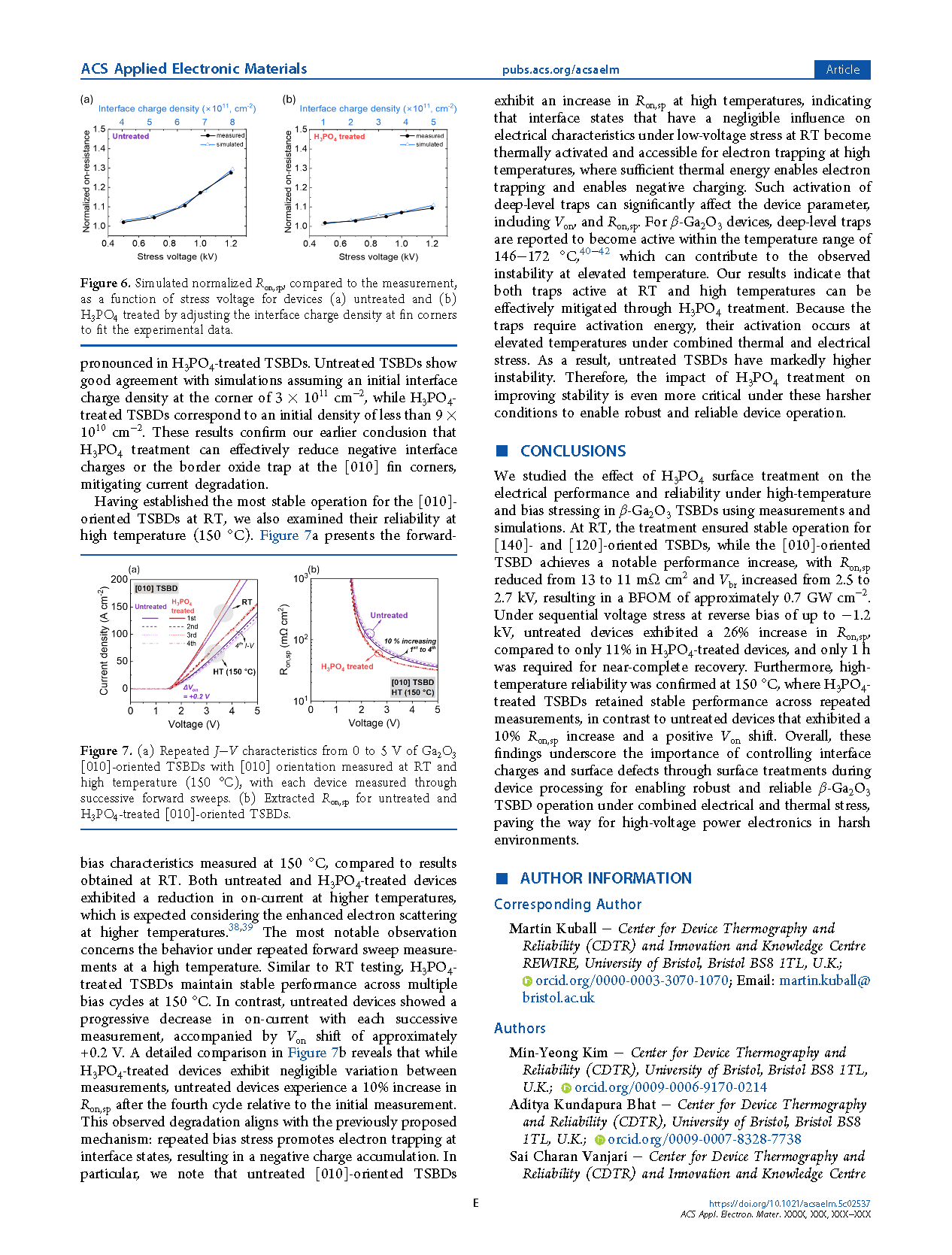
Figure 6. Simulated normalized Ron,sp, compared to the measurement, as a function of stress voltage for devices (a) untreated and (b) H3PO4 treated by adjusting the interface charge density at fin corners to fit the experimental data.
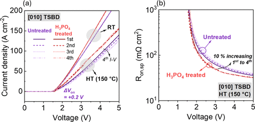
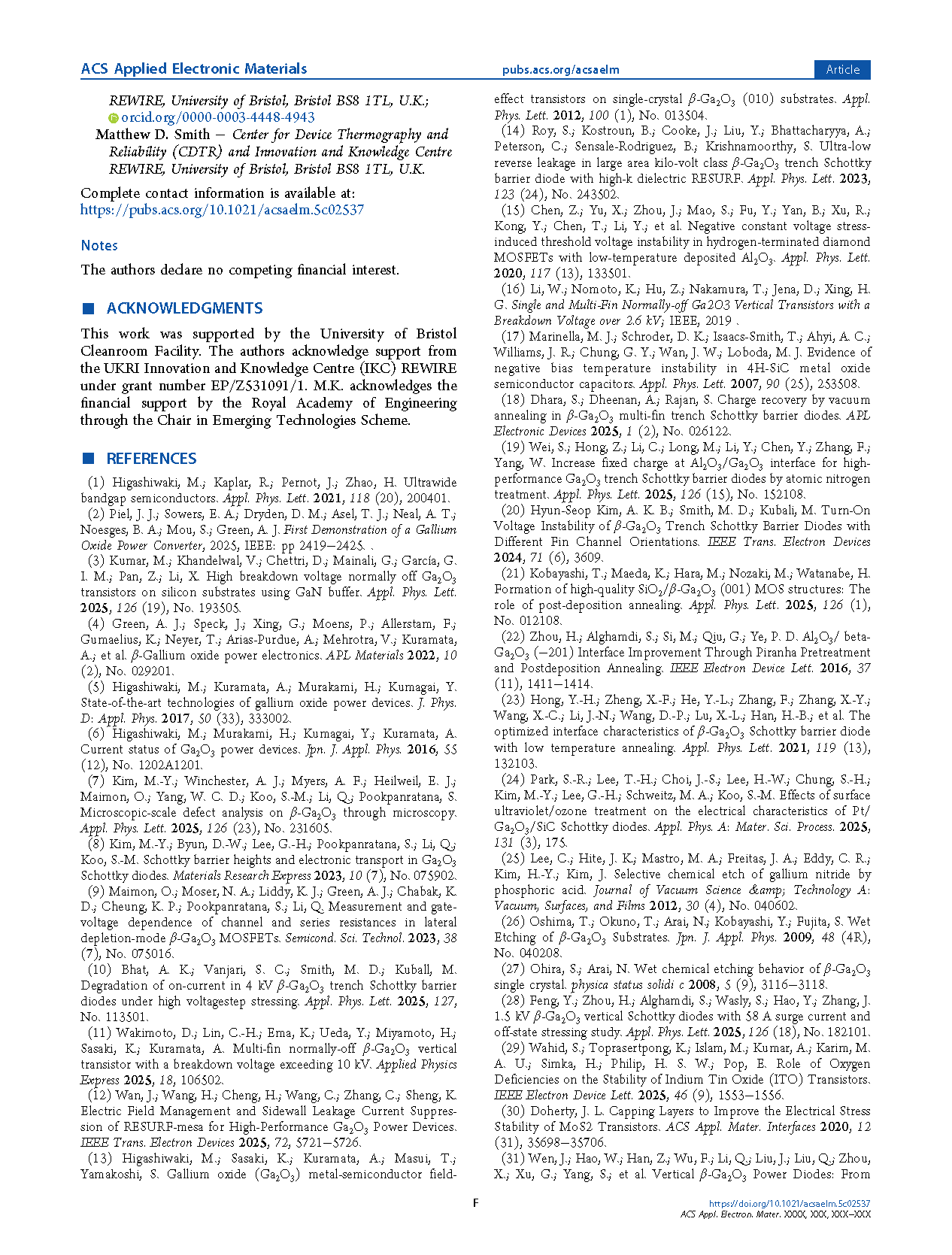
Figure 7. (a) Repeated J–V characteristics from 0 to 5 V of Ga2O3 [010]-oriented TSBDs with [010] orientation measured at RT and high temperature (150 °C), with each device measured through successive forward sweeps. (b) Extracted Ron,sp for untreated and H3PO4-treated [010]-oriented TSBDs.
DOI:
doi.org/10.1021/acsaelm.5c02537