Paper Sharing
【Member Papers】Bond-angle modulation in nucleation layer overcomes lattice-mismatch limits in Ga₂O₃ heteroepitaxy
日期:2026-03-17阅读:381
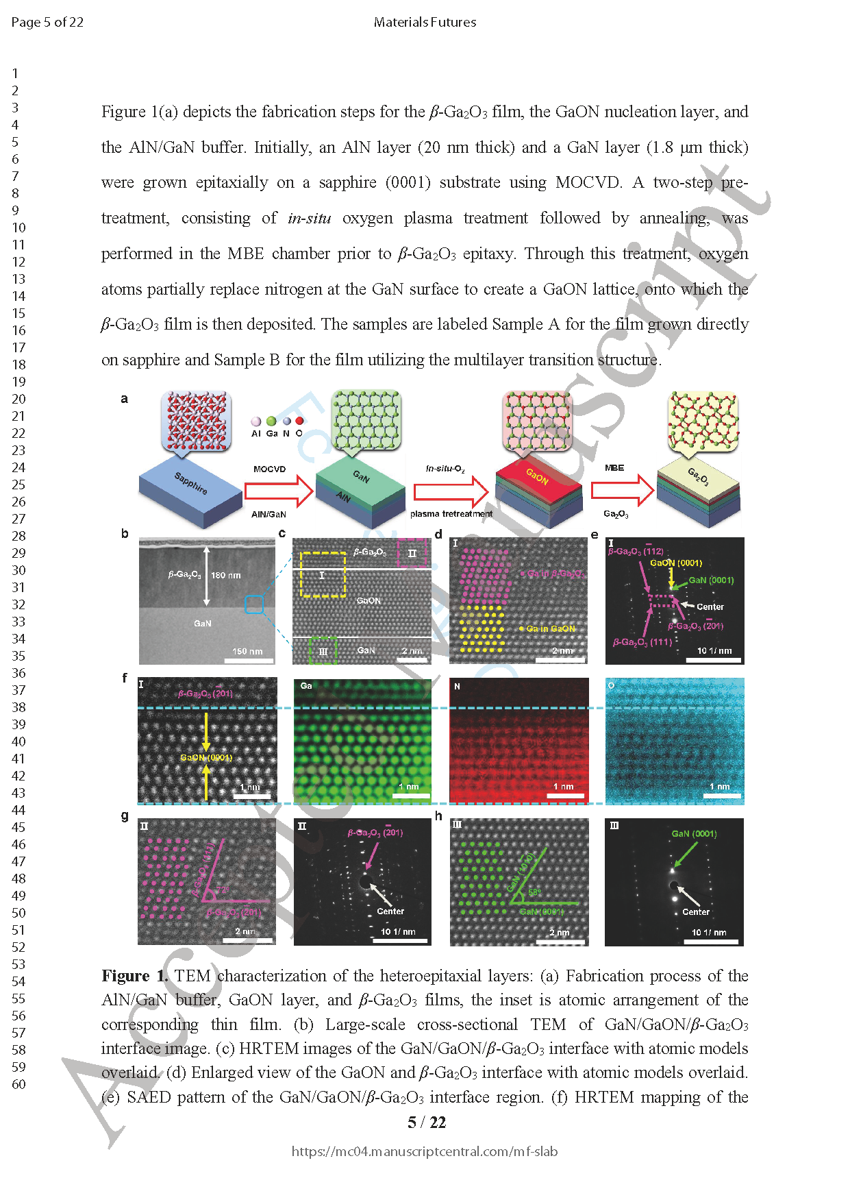
Researchers from the Xiamen University have published a dissertation titled "Bond-angle modulation in nucleation layer overcomes lattice-mismatch limits in Ga2O3 heteroepitaxy" in Materials Futures.
Background
β-Ga₂O₃ is an ideal material for high-power electronic devices and deep-ultraviolet optoelectronic applications due to its ultra-wide bandgap (~4.9 eV), high breakdown electric field (8 MV/cm), and excellent Baliga's figure of merit. However, the high cost and poor thermal properties of bulk single-crystal substrates make heteroepitaxial growth a critical pathway for its application. During heteroepitaxy, lattice mismatch and interfacial stress lead to high defect densities, severely limiting device performance. Traditional buffer layers like GaN can partially mitigate the mismatch, but issues like residual strain and interface disorder persist. Recently, gallium oxynitride (GaON) has been preliminarily explored as a nucleation layer, but its atomic-scale structure, nucleation mechanism, and influence on band structure and carrier dynamics remain unclear.
Abstract
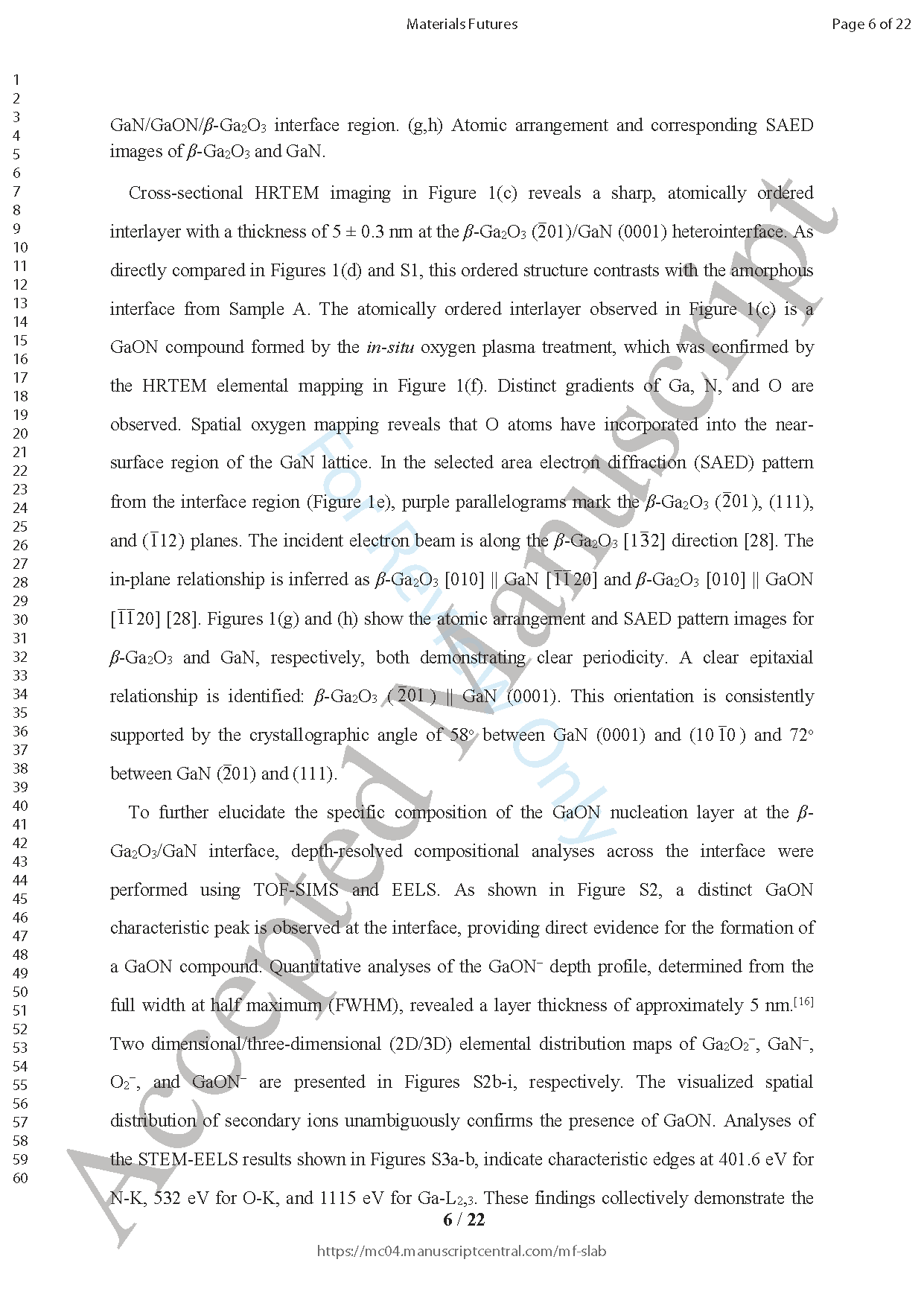
This study demonstrates a multilayer transition strategy for growing high-quality β-Ga₂O₃ thin films on sapphire substrates via plasma-assisted molecular beam epitaxy (PAMBE). The structure incorporates an AlN/GaN buffer layer and a GaON nucleation layer formed by in-situ oxygen plasma treatment. First-principles calculations reveal the mechanism of GaON as an effective nucleation layer: its N-Ga-O bond angle (90.27°) closely matches the average bond angle (90.4°) of GaO₆ octahedra in β-Ga₂O₃, and its effective plane energy (0.109 eV/Ų) is significantly lower than that of sapphire (0.218 eV/Ų), promoting heterogeneous nucleation.
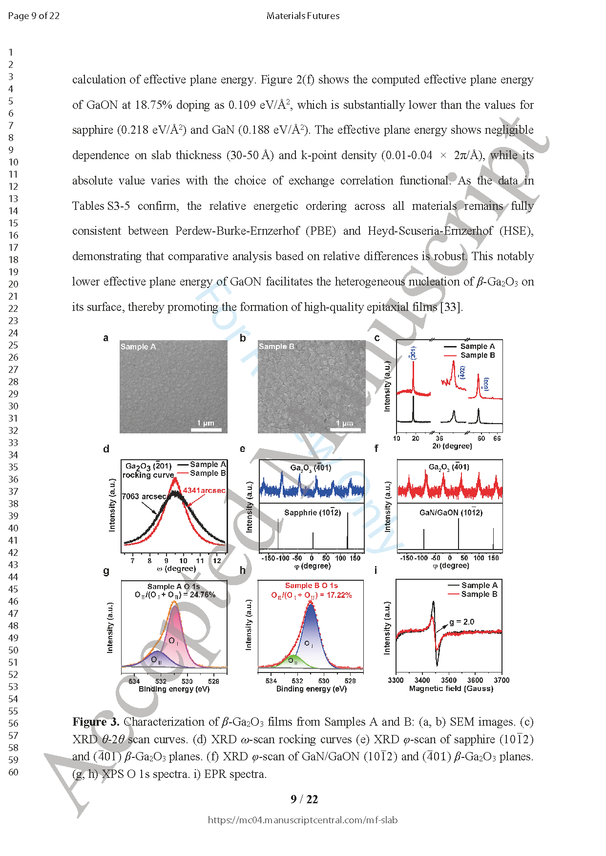
Experimental results show the GaON layer is approximately 5 nm thick with an oxygen gradient, transitioning from GaO₀.₁₇N₀.₈₃ at the outer region to GaN deeper within. HRTEM confirms this layer is atomically ordered, contrasting with the amorphous interface in samples without GaON. XRD analysis shows that introducing the GaON layer reduces the rocking curve FWHM of the β-Ga₂O₃ film from 7063 to 4341 arcsec, decreasing screw dislocation density by about 62%. XPS and EPR analyses further confirm that the GaON layer effectively suppresses oxygen vacancy defects.
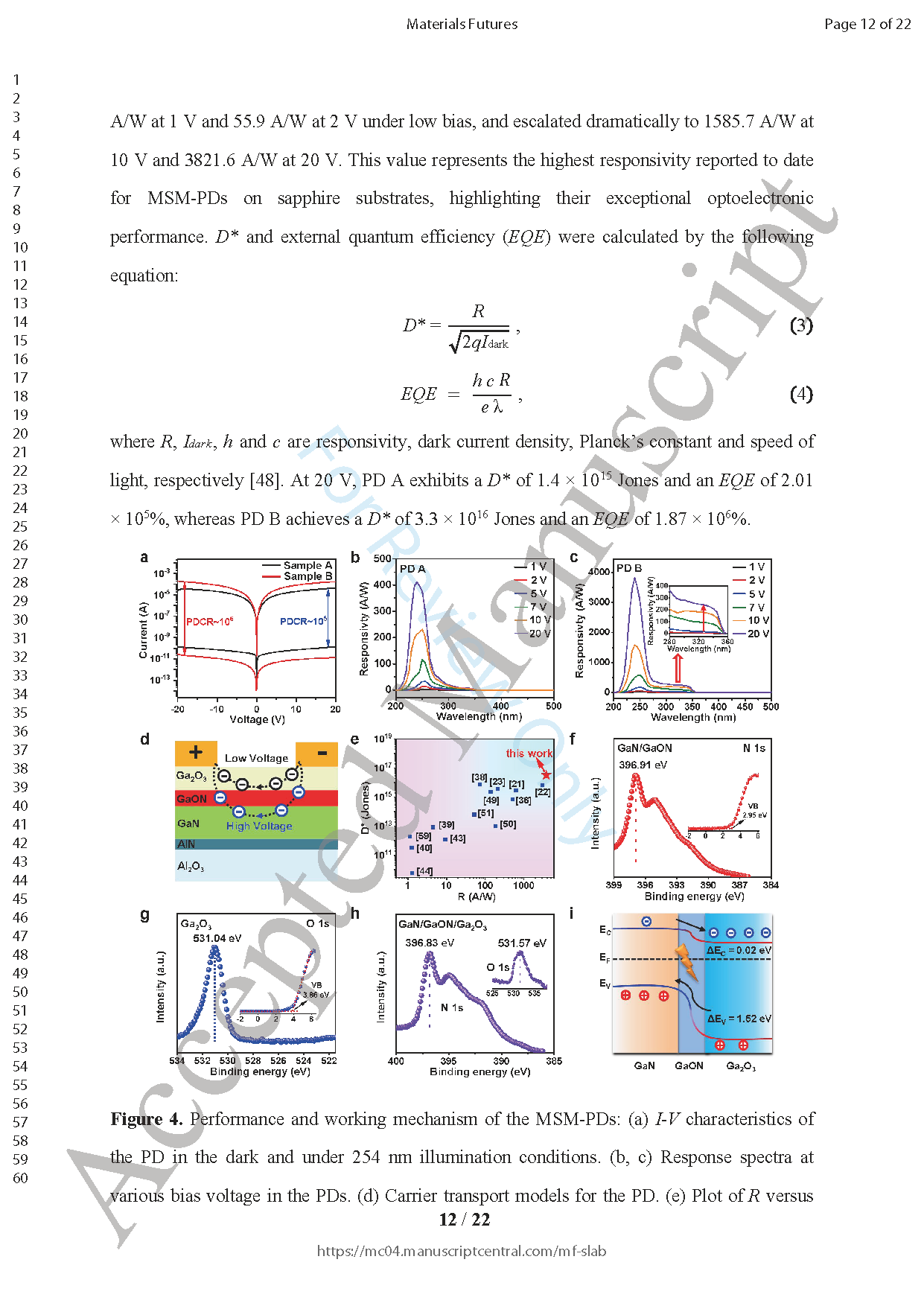
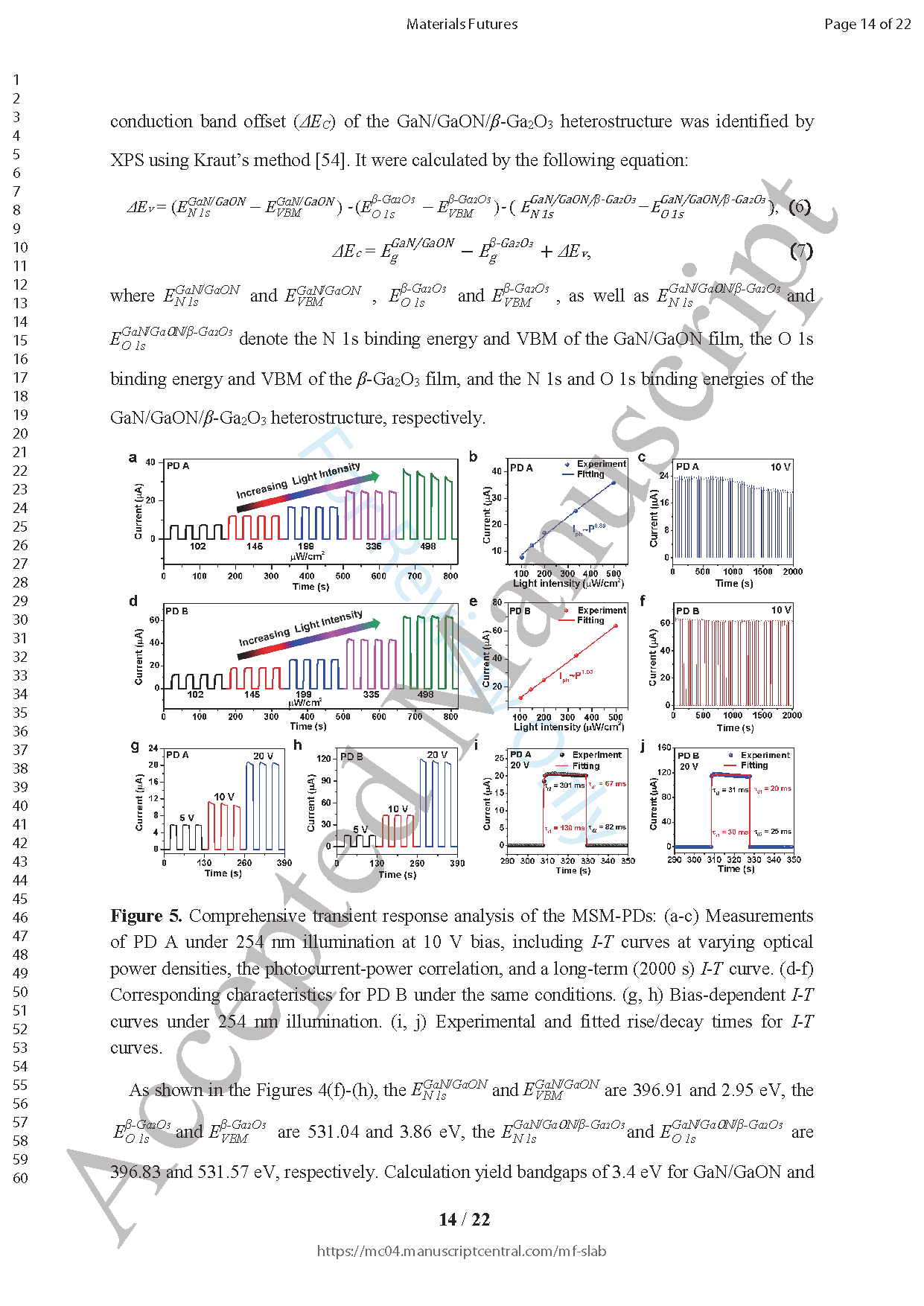
At the device level, metal-semiconductor-metal photodetectors (MSM-PDs) based on this structure exhibit excellent performance under 254 nm illumination: an ultra-low dark current of 13 pA, a photo-to-dark current ratio of 6.29×10⁶, a high responsivity of 3821.6 A/W, a high specific detectivity of 3.3×10¹⁶ Jones, and fast response times (rise/decay: 30/20 ms). Band structure analysis reveals that the GaON layer creates a smooth band transition from GaN to β-Ga₂O₃, reducing the valence band offset from 1.7 eV to 1.52 eV and the conduction band offset from 0.12 eV to 0.02 eV, significantly enhancing carrier extraction efficiency.
Highlights
Proposes and validates a bond-angle-matched GaON nucleation layer design strategy, overcoming traditional lattice-matching limitations.
First to combine DFT calculations with experiments to reveal the oxygen-gradient structure of GaON and its role in mitigating lattice strain.
The GaON layer not only improves crystal quality but also achieves a graded energy band, significantly optimizing carrier transport.
The fabricated MSM ultraviolet photodetectors achieve world-leading performance in key metrics like responsivity, detectivity, and response speed.
Conclusion
This research successfully achieved high-quality heteroepitaxial growth of β-Ga₂O₃ thin films on sapphire substrates by introducing a GaON nucleation layer within an AlN/GaN multilayer buffer structure. The GaON layer, with its bond-angle compatibility with β-Ga₂O₃ and low effective plane energy, effectively mitigates stress and defects caused by lattice mismatch. Band analysis further indicates that the GaON layer enables a smooth band transition from GaN to β-Ga₂O₃, improving carrier separation efficiency. The resulting ultraviolet photodetectors demonstrate excellent performance across multiple metrics, validating the universality and application potential of this strategy for heteroepitaxy of wide-bandgap semiconductors.
Project Support
This work was supported the National Natural Science Foundation of China (Grant No. 62171396), the Shenzhen Science and Technology Program (Grant No. JCYJ20240813145617023), the Central University Basic Research Fund of China under (Grant No. 20720230040), Fujian Minjiang Distinguished Scholar Program, and Xiamen Double Hundred-Talent Program.
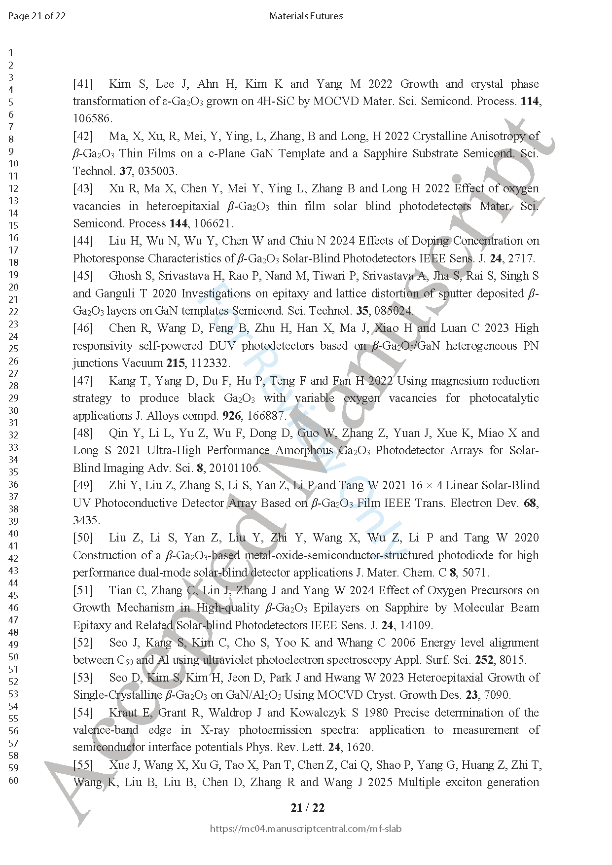
Figure 1. TEM characterization of the heteroepitaxial layers: (a) Fabrication process of the AlN/GaN buffer, GaON layer, and β-Ga₂O₃ films, the inset is atomic arrangement of the corresponding thin film. (b) Large-scale cross-sectional TEM of GaN/GaON/β-Ga₂O₃ interface image. (c) HRTEM images of the GaN/GaON/β-Ga₂O₃ interface with atomic models overlaid. (d) Enlarged view of the GaON and β-Ga₂O₃ interface with atomic models overlaid. (e) SAED pattern of the GaN/GaON/β-Ga₂O₃ interface region. (f) HRTEM mapping of the GaN/GaON/β-Ga₂O₃ interface region. (g,h) Atomic arrangement and corresponding SAED images of β-Ga₂O₃ and GaN.
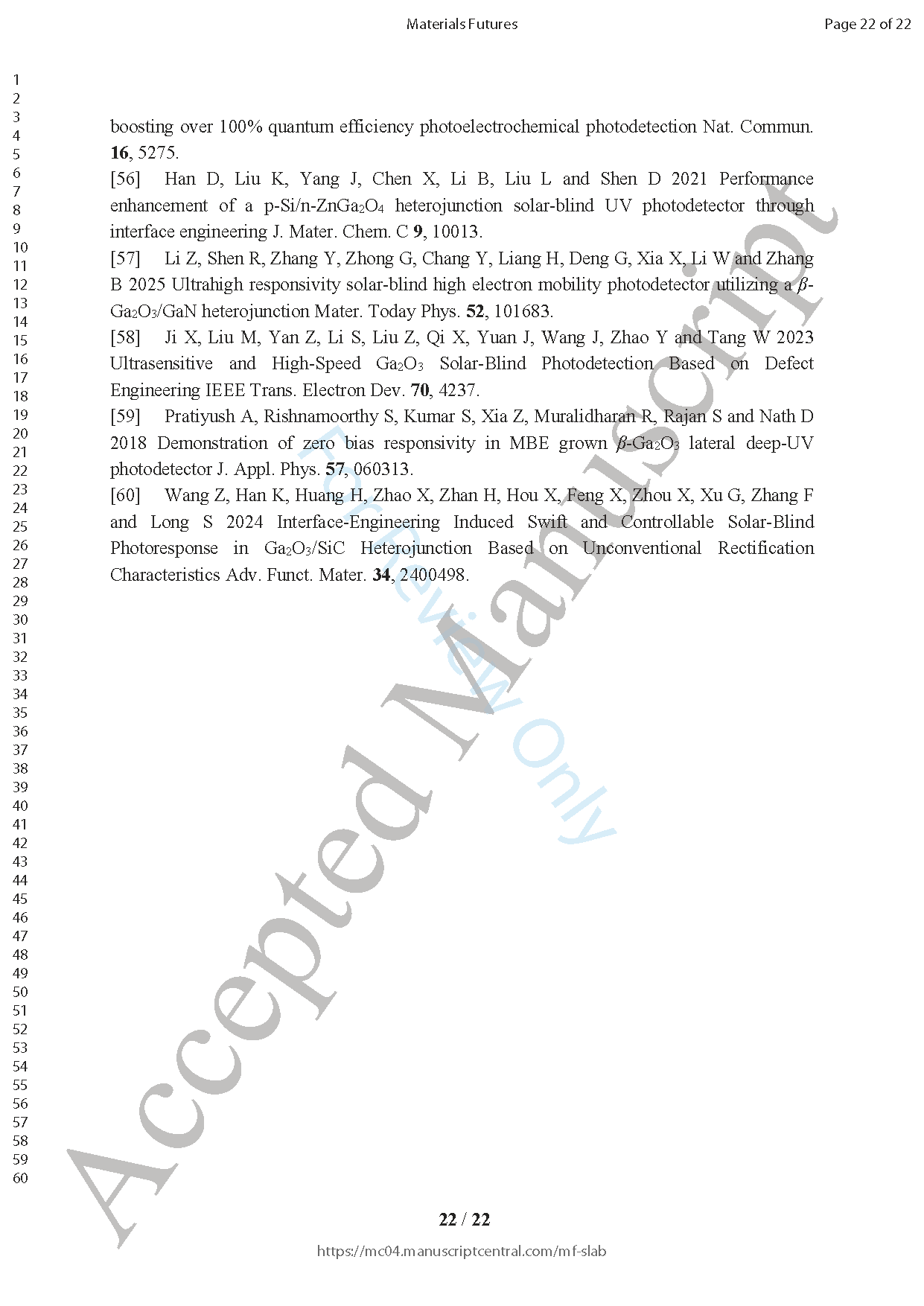
Figure 2. First-principles calculations of the GaON Nucleation Layer: (a) 5-nm-thick GaON with oxygen gradient HRTEM image. (b) Interplanar spacing of GaN and GaO₀.₁₇N₀.₈₃. (c) Model of GaN supercell structure (a = b = 6.436 Å, c = 10.483 Å) and the distance of interlayer is 1.975 Å. (d) The lattice constant as a function of oxygen concentration. (e) Bond angles (N-Ga-N and N-Ga-O) versus oxygen concentration. (f) The effective plane energy of Sapphire, GaN, and GaON with varying oxygen concentrations (GaO₀.₀₆N₀.₉₄, GaO₀.₁₃N₀.₈₇ and GaO₀.₁₉N₀.₈₁).
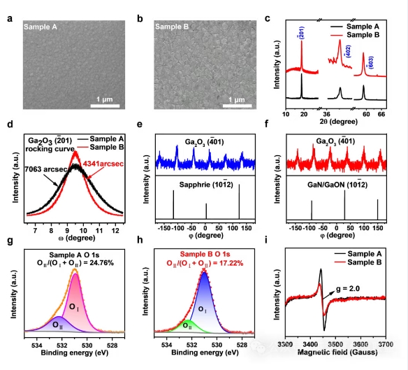
Figure 3. Characterization of β-Ga₂O₃ films from Samples A and B: (a, b) SEM images. (c) XRD θ-2θ scan curves. (d) XRD ω-scan rocking curves. (e) XRD φ-scan of sapphire (101-12) and (401) β-Ga₂O₃ planes. (f) XRD φ-scan of GaN/GaON (101-12) and (-401) β-Ga₂O₃ planes. (g, h) XPS O 1s spectra. (i) EPR spectra.
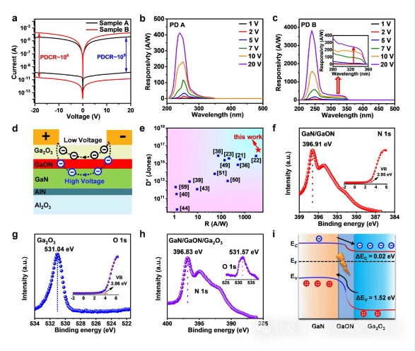
Figure 4. Performance and working mechanism of the MSM-PDs: (a) I-V characteristics of the PD in the dark and under 254 nm illumination conditions. (b, c) Response spectra at various bias voltage in the PDs. (d) Carrier transport models for the PD. (e) Plot of R versus D* for our PDs against the reported β-Ga2O3 MSM-PDs on sapphire substrates. (f) N 1s XPS and valence band spectra from the GaN/GaON film. (g) O 1s XPS and valence band spectra from the B-Ga2O3 film. (h) N 1s and O 1s core levels of the GaN/GaON/ß-Ga2O3 heterostructure. (i) Corresponding energy band diagrams.
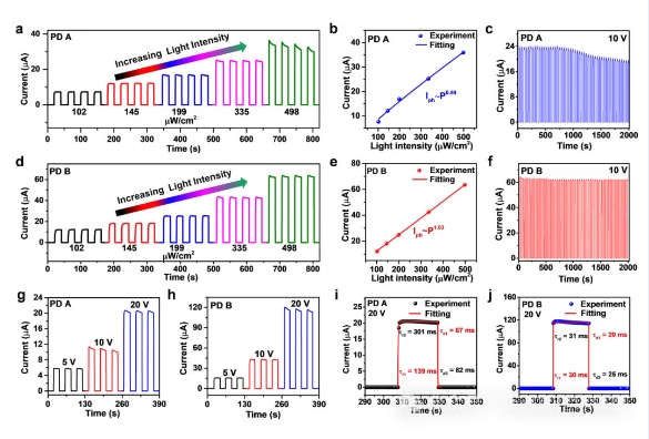
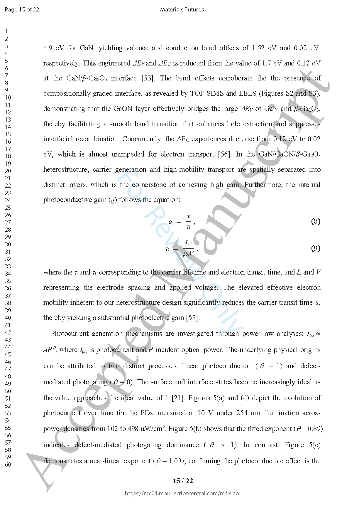
Figure 5. Comprehensive transient response analysis of the MSM-PDs: (a-c) Measurements of PD A under 254 nm illumination at 10 V bias, including I-T curves at varying optical power densities, the photocurrent-power correlation, and a long-term (2000 s) I-T curve. (d-f) Corresponding characteristics for PD B under the same conditions. (g, h) Bias-dependent I-T curves under 254 nm illumination. (i, j) Experimental and fitted rise/decay times for I-T curves.
DOI:
10.1088/2752-5724/ae4e4c