


Paper Sharing
【Member Papers】Ultrathin GaOx Tunneling Contact for 2D Transition-metal Dichalcogenides Transistor
日期:2026-03-18阅读:257
Two-dimensional (2D) semiconductor materials hold critical strategic significance for the development of integrated circuits in the post-Moore era, yet their device performance has long been constrained by Schottky barriers and Fermi level pinning at metal–semiconductor interfaces. To address this fundamental challenge, a joint team comprising Researcher Lin Shenghuang from Songshan Lake Materials Laboratory, Researcher Zhang Guangyu from Songshan Lake Materials Laboratory/Institute of Physics, Chinese Academy of Sciences, Associate Researcher Cui Nan from Songshan Lake Materials Laboratory, and Professor Zhang Song from Wuhan University of Technology, has innovatively developed a printable ultrathin gallium oxide (GaOx) tunneling contact technology. The team systematically revealed a defect-mediated tunneling transport mechanism controlled by oxygen vacancies, and simultaneously achieved high carrier mobility, low contact resistance, and low barrier height in multilayer tungsten disulfide (WS₂) field-effect transistors (FETs). This study provides a new physical picture and fabrication paradigm for transforming tunneling contacts from a “passive insulating layer” to a “functionalized injection interface.” The related results were published in International Journal of Extreme Manufacturing, with Songshan Lake Materials Laboratory as a co-corresponding institution.
The core innovation of this work lies in proposing and validating a novel contact engineering strategy for 2D transistors based on a printable ultrathin GaOx tunneling layer. The team utilized the self-limiting oxidation characteristic of liquid gallium to fabricate an ultrathin GaOx film with a thickness of only ~3.6 nm, and for the first time functionally applied it as an active tunneling contact layer in 2D semiconductor devices. Unlike conventional insulating tunneling dielectrics such as hBN, the controllably introduced oxygen vacancy defect states in the GaOx layer significantly reduce the effective tunneling barrier width, thereby establishing a low-barrier, high-tunneling-probability carrier injection channel between the metal and the WS₂ channel.
The study shows that carrier transport through the GaOx tunneling contact is not dominated by a single tunneling mechanism; rather, under the combined influence of electric field and temperature, a defect-mediated composite tunneling transport mechanism is activated. This mechanism involves the synergistic contribution of defect-assisted tunneling, direct tunneling, and Fowler–Nordheim tunneling. This unique hybrid tunneling behavior enables the device to simultaneously achieve ultralow contact resistance (2.38 kΩ·μm), extremely low contact barrier (3.7 meV), and a record-high electron mobility in multilayer WS₂ (296 cm²·V⁻¹·s⁻¹).
Moreover, the GaOx tunneling layer is fabricated using a low-temperature liquid-metal printing process, forming a van der Waals integrated interface with the 2D material. This approach effectively circumvents the Fermi level pinning issue while exhibiting excellent large-area uniformity and device stability. This work not only elucidates the critical physical role of oxygen vacancies in tunneling modulation within ultrathin GaOx, but also provides a new scalable and low-thermal-budget pathway for achieving high-performance contacts in low-dimensional electronic devices.
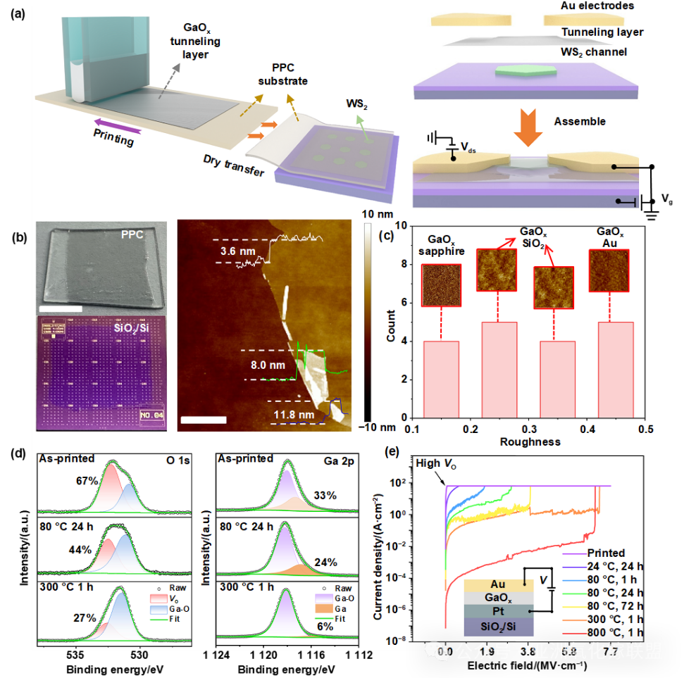
Figure 1. Structural and performance characterization of the printed atomically thin GaOx layer
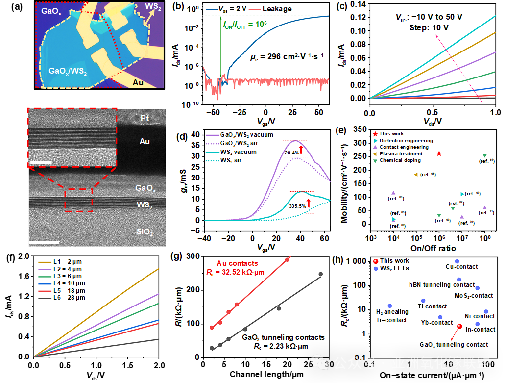
Figure 2. Room-temperature electrical performance characterization of the devices
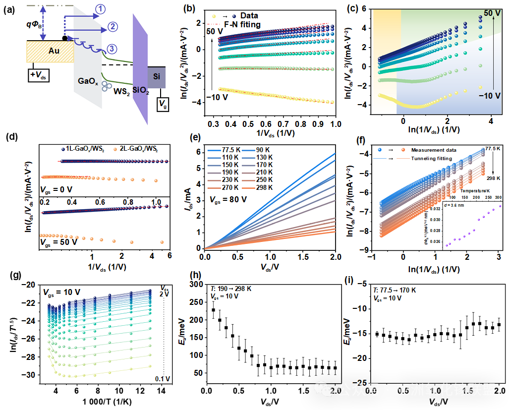
Figure 3. Analysis of the electron tunneling mechanism in the GaOx layer
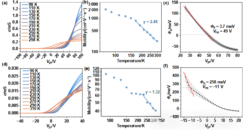
Figure 4. Temperature-dependent characterization and analysis of the devices
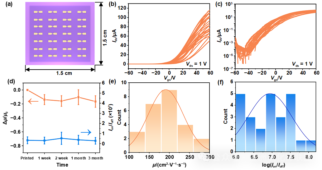
Figure 5. Statistical analysis of tunneling-contact transistor device performance
By introducing a printable ultrathin GaOx tunneling layer, this work systematically reveals the composite tunneling transport mechanism modulated by oxygen vacancies and achieves synergistic optimization of high mobility, low contact resistance, and low barrier height in multilayer WS₂ field-effect transistors (FETs). This study not only overcomes the conventional bottleneck in two-dimensional devices where metal–semiconductor contacts are limited by Schottky barriers and Fermi level pinning but also provides a new physical perspective and processing paradigm for transforming tunneling contacts from “passive insulating layers” to “functional injection interfaces.” Overall, this low-temperature, printable GaOx fabrication approach offers a new strategy and a practical technical pathway for large-area integration, flexible electronics, and back-end-compatible manufacturing.
DOI:doi.org/10.1088/2631-7990/ae51d2
