Paper Sharing
【Domestic Papers】Research on nitrogen annealing of V-doped β-Ga₂O₃ single crystals grown by EFG
日期:2026-03-18阅读:285
Researchers from the Micius Laboratory and Shanghai Institute of Optics and Fine Mechanics have published a dissertation titled "Research on nitrogen annealing of V-doped β-Ga2O3 single crystals grown by EFG" in Journal of Alloys and Compounds.
Project Support
This work is supported by the National Natural Science Foundation of China (Grant No. 52488301), and Shanghai Strategic Frontier Special Project (Grant No. 24DP1500100). The authors also thank Hangzhou Fujia Gallium Technology Co., Ltd. for helping in crystal growth and processing.
Background
Ultra-wide bandgap semiconductors have progressed rapidly due to their ability to meet stringent requirements in extreme environments, including high voltage, high temperature, and strong corrosion―conditions where traditional silicon materials fall short. Emerging monoclinic beta-phase gallium oxide (β-Ga2O3) has garnered significant attention due to its exceptional properties: an ultra-wide bandgap (Eg ≃ 4.9 eV), high estimated critical electric field (Ec ≃ 8 MV cm–1), and high Baliga’s figure of merit (BFOM ≃ 3400). The potential for large-scale commercial production of single-crystal substrates positions β-Ga2O3 as an ideal candidate material for high-power, high-efficiency electronic devices and solar-blind photodetectors. These applications demand exceptionally high standards across all aspects of the core single-crystal substrates.
Abstract
The regulation of electrical and optical properties in ultra-wide bandgap beta-gallium oxide (β-Ga2O3) through the introduction of dopants and thermal annealing has been a focal point in semiconductor research. Herein, a high-quality V-doped β-Ga2O3 crystal was synthesized using the edge-defined film-fed growth (EFG) technique. A variety of characterization methods were employed to systematically examine changes in the crystal structural, optical, and electrical properties of the V-doped β-Ga2O3 before and after annealing in an N2 atmosphere. Annealing treatment significantly improved crystal quality. Following N2 annealing, carrier concentration reduced rather than enhanced, infrared region transmittance increased, and mid-to-high frequency Raman phonon peak intensities were altered, which were ascribed to the formation of Ga vacancies, the destruction of carbon DX centers, and the capture of electrons by interstitial Ga. Variations in the concentrations of interstitial Ga and Ga vacancy led to an enlargement in the area ratio of the blue luminescence peak. These findings provide deeper insight into the effects of N2 annealing on the crystal structure and properties of V-doped β-Ga2O3.
Conclusions
In summary, the 2-inch V-doped β-Ga2O3 single crystal with (100) plane was grown by the EFG technique. Rocking curves, Hall effect, XPS, optical transmittance, Raman spectroscopy, and PL properties were performed on samples before and after N2 heat treatment. The FWHM values of 39.6″ and 28.8″ demonstrate that the crystalline quality of the annealed crystals was superior to that of the unannealed ones. The post-annealing decline in free electron concentration, enhancement in near-infrared transmittance, and variation in Raman peak intensity can be explained by the formation of VGa as the deep acceptor and the disruption of carbon DX centers as the shallow donor by introduced N atoms. Concurrently, Gai (Ga3+) trapped electrons and converted to Ga2+, further contributing to the reduction in carrier concentration after annealing. Room-temperature PL spectra reveal an increased proportion of blue emission peaks following N2 annealing, attributable to heightened concentrations of Gai and VGa.
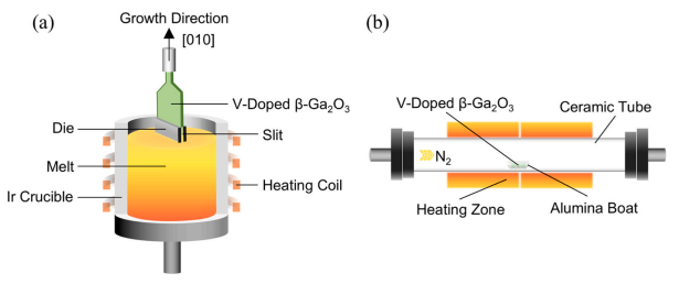
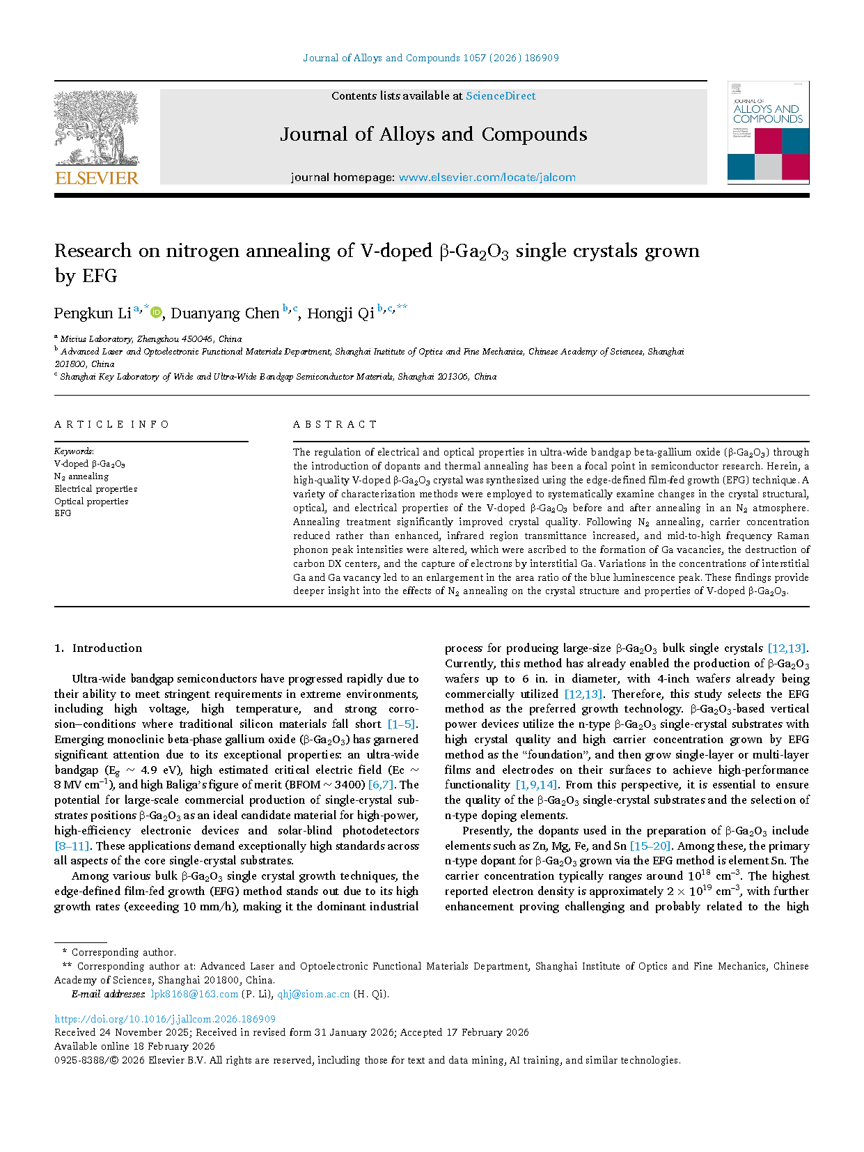
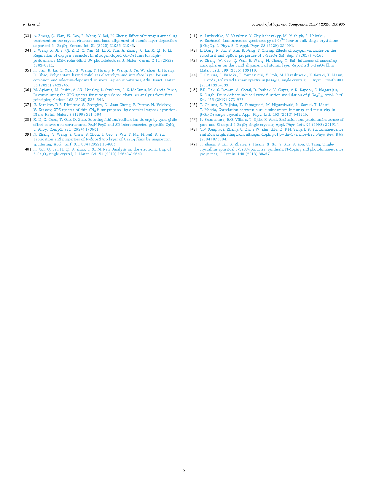
Fig. 1. (a) EFG apparatus and (b) tube furnace for β-Ga2O3 bulk single crystal growth and annealing.
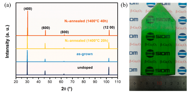
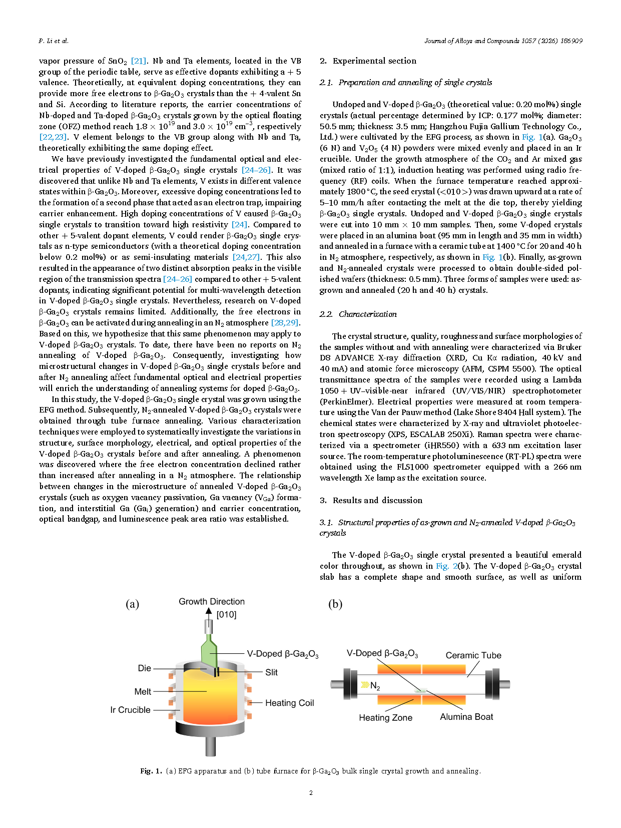
Fig. 2. (a) High-resolution XRD patterns of undoped and V-doped β-Ga2O3 crystals. (b) Photograph of 2-inch V-doped β-Ga2O3 crystal.
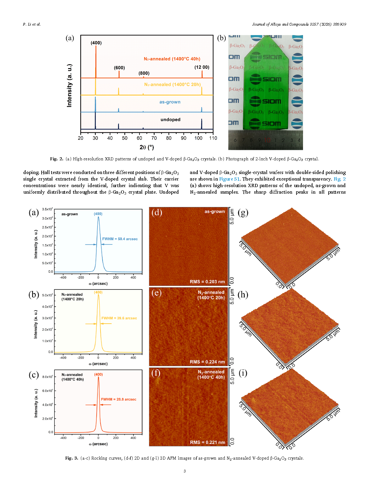
Fig. 3. (a-c) Rocking curves, (d-f) 2D and (g-i) 3D AFM images of as-grown and N2-annealed V-doped β-Ga2O3 crystals.
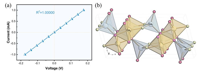
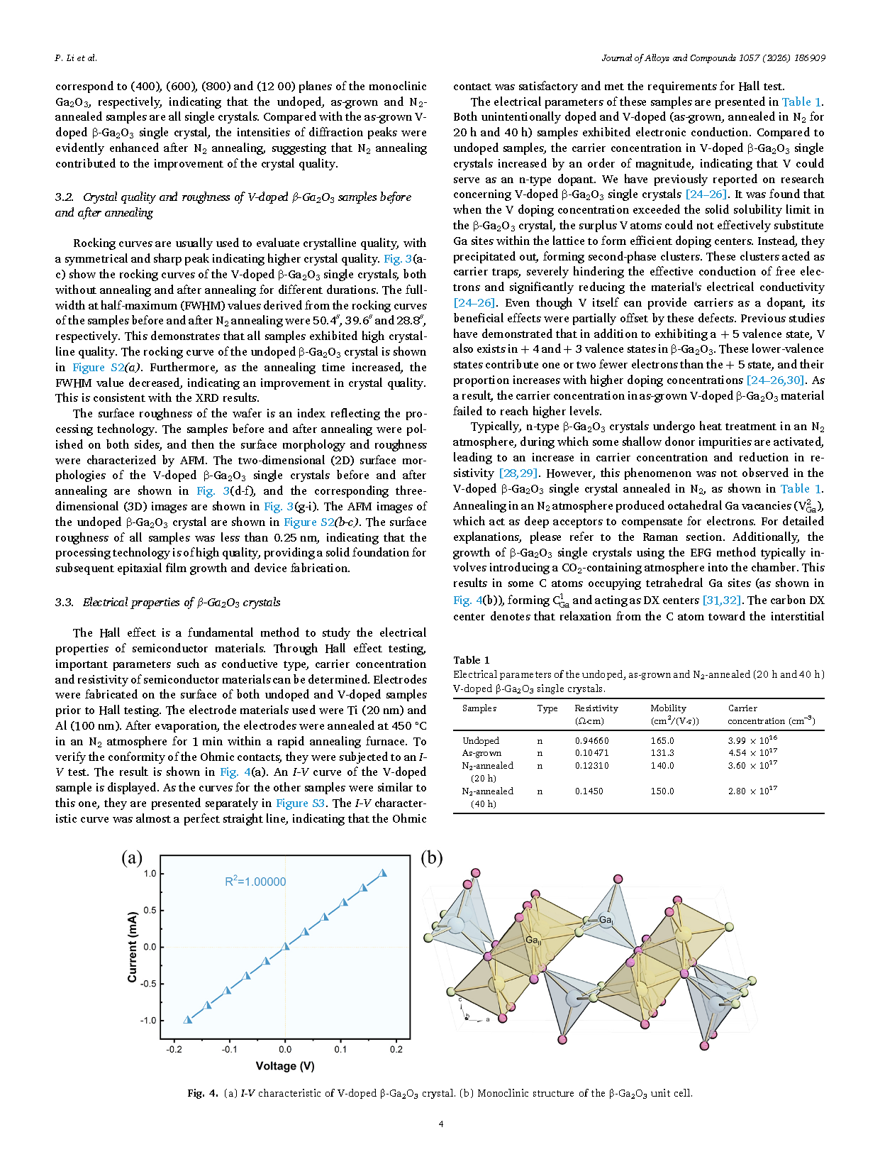
Fig. 4. (a) I-V characteristic of V-doped β-Ga2O3 crystal. (b) Monoclinic structure of the β-Ga2O3 unit cell.
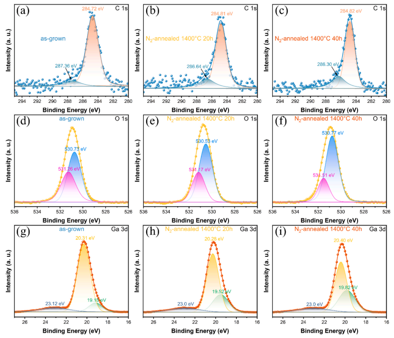
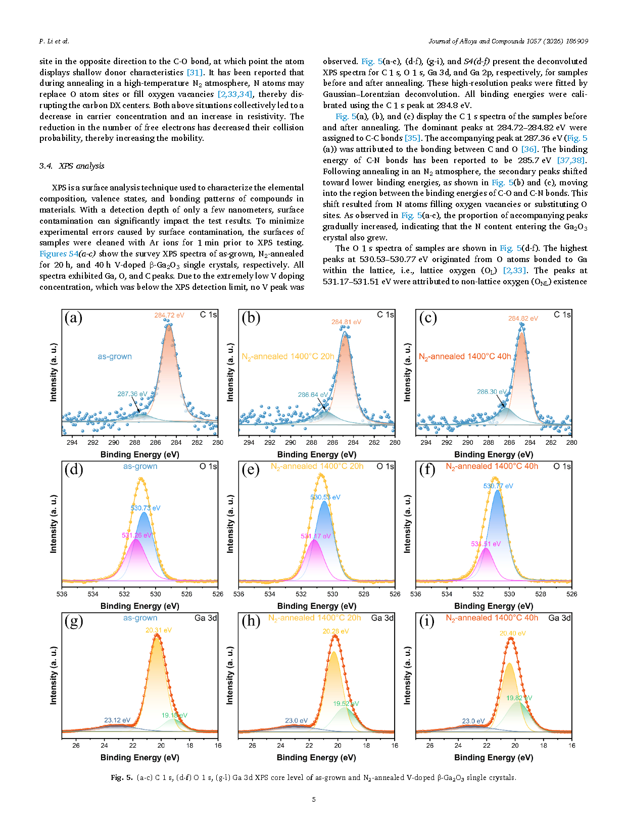
Fig. 5. (a-c) C 1 s, (d-f) O 1 s, (g-i) Ga 3d XPS core level of as-grown and N2-annealed V-doped β-Ga2O3 single crystals.
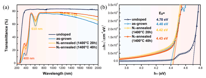
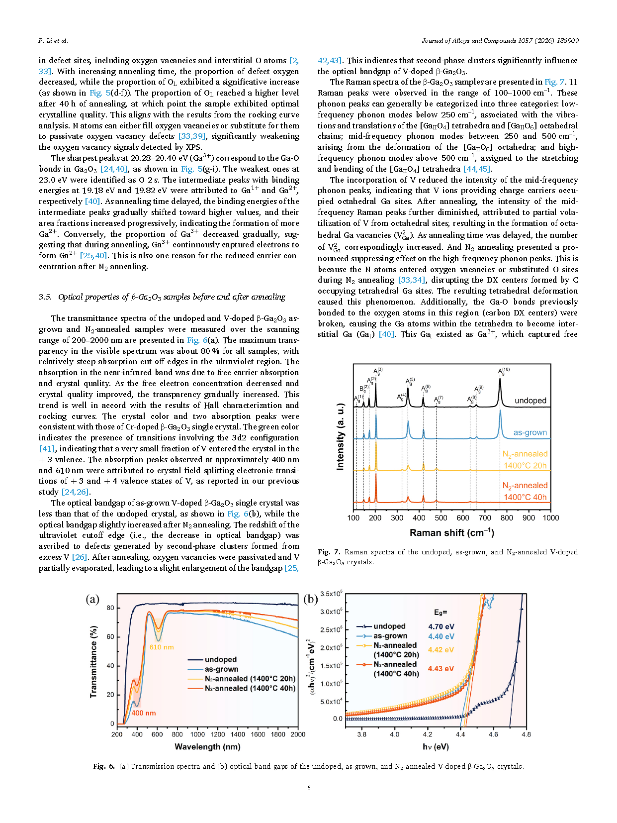
Fig. 6. (a) Transmission spectra and (b) optical band gaps of the undoped, as-grown, and N2-annealed V-doped β-Ga2O3 crystals.
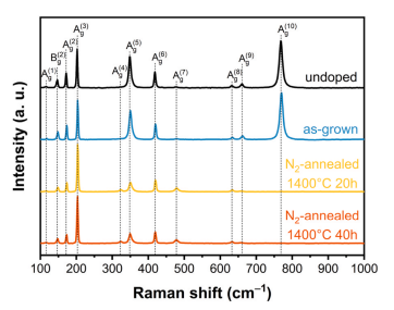
Fig. 7. Raman spectra of the undoped, as-grown, and N2-annealed V-doped β-Ga2O3 crystals.
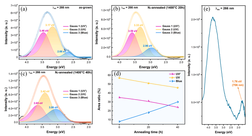
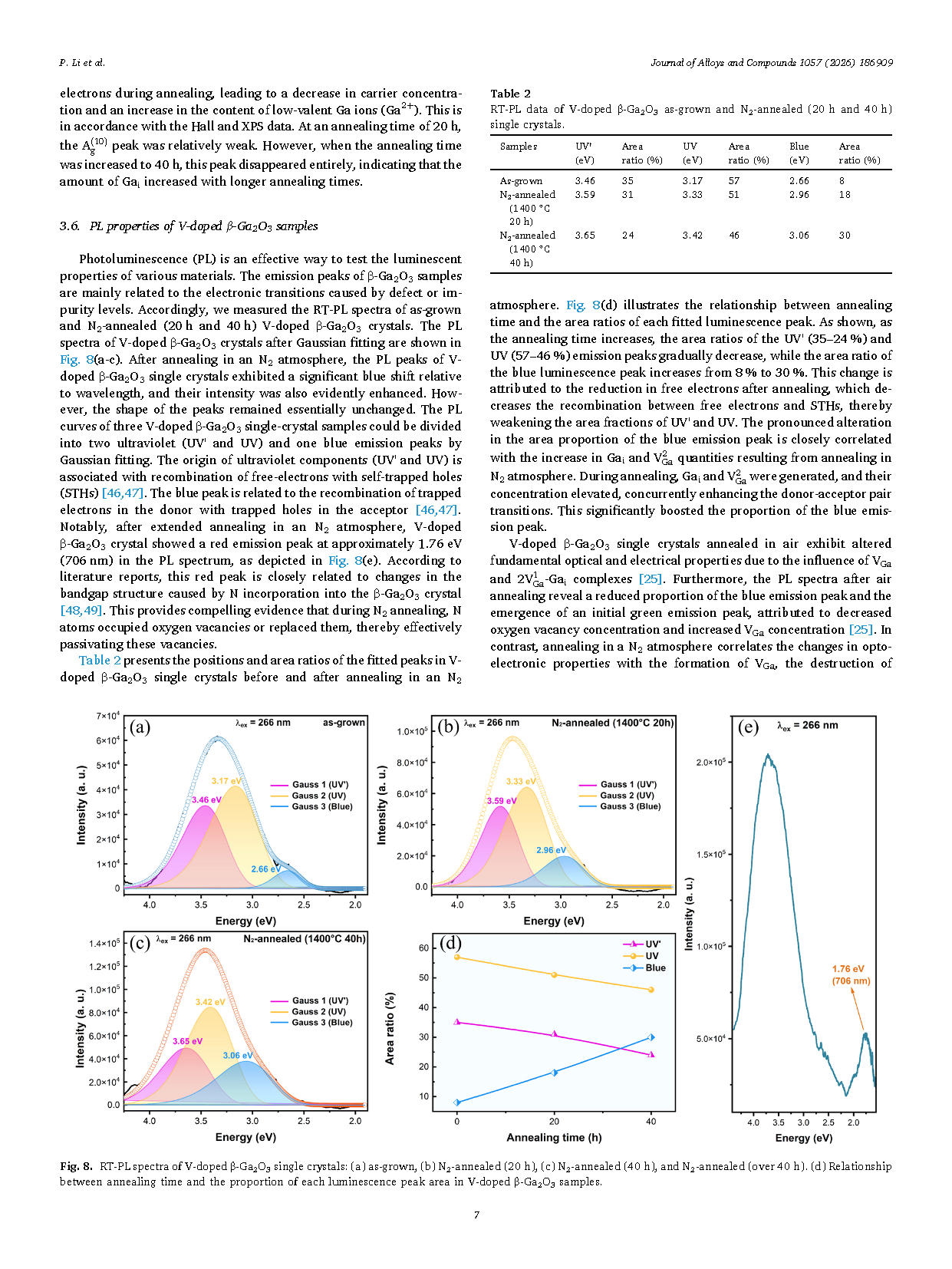
Fig. 8. RT-PL spectra of V-doped β-Ga2O3 single crystals: (a) as-grown, (b) N2-annealed (20 h), (c) N2-annealed (40 h), and N2-annealed (over 40 h). (d) Relationship between annealing time and the proportion of each luminescence peak area in V-doped β-Ga2O3 samples.
DOI:
doi.org/10.1016/j.jallcom.2026.186909