Paper Sharing
【Member Papers】Theoretical study of polarity-driven interfacial engineering for high-performance β-Ga₂O₃ optoelectronic devices
日期:2026-03-18阅读:288
Researchers from the Xidian University have published a dissertation titled "Theoretical study of polarity-driven interfacial engineering for high-performance β-Ga2O3 optoelectronic devices" in Journal of Alloys and Compounds.
Project Support
This work was financially supported by the National Natural Science Foundation of China (62404170, 62274127, 62421005), National Key Research and Development Program of China (2021YFA0715600, 2021YFA0717700), China Postdoctoral Science Foundation (2023TQ0255), Postdoctoral Fellowship Program of CPSF (GZB20230562), Guangdong Basic and Applied Basic Research Fund (2024B1515120035), Fundamental Research Funds for the Central Universities. The numerical calculations in this paper have been done on the HPC system of XIDIAN University.
Background
Recently, β-Ga2O3 has drawn extensive attention due to the intrinsic naturally wide bandgap (∼4.9 eV), large critical-breakdown electric field (∼8 MV/cm), high Baliga’s figure of merit (over 3000), high chemical and thermal stability, which make β-Ga2O3 widely used in the harsh environmental field such as astronautical exploration. Meanwhile, the low-cost β-Ga2O3 single crystal growth techniques, such as Czochralski method and chemical vapor deposition, have significantly advanced the development of Ga2O3-based electronic devices, particularly solar-blind photodetectors, including photodiode, phototransistor, metal-semiconductor-metal photodetector, avalanche photodetector and unipolar barrier avalanche photodetector. However, limited by the low carrier mobility, strong exciton recombination and poor thermal conductivity for natural β-Ga2O3 crystal, the performances of those devices are still far away from a practical application.
Abstract
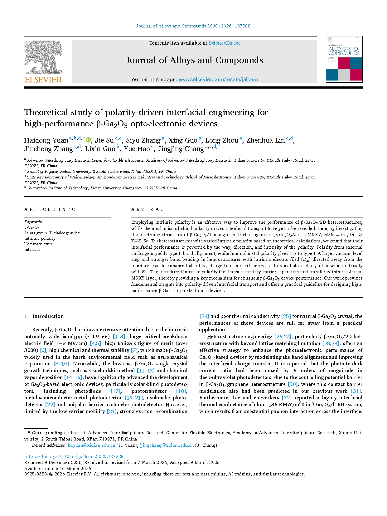
Employing intrinsic polarity is an effective way to improve the performance of β-Ga2O3/2D heterostructures, while the mechanisms behind polarity-driven interfacial transport have yet to be revealed. Here, by investigating the electronic structures of β-Ga2O3/Janus group-III chalcogenides (β-Ga2O3/Janus-MNXY, M/N = Ga, In; X/YS, Se, Te) heterostructures with varied intrinsic polarity based on theoretical calculations, we found that their interfacial performance is governed by the way, direction, and intensity of the polarity. Polarity from external chalcogens yields type-II band alignment, while internal metal polarity gives rise to type-I. A larger vacuum level step and stronger band bending in heterostructures with intrinsic electric filed (Ein) directed away from the interface lead to enhanced stability, charge transport efficiency, and optical absorption, all of which intensify with Ein. The introduced intrinsic polarity facilitates secondary carrier separation and transfer within the Janus-MNXY layer, thereby providing a key mechanism for enhancing β-Ga2O3 device performance. Our work provides fundamental insights into polarity-driven interfacial transport and offers a practical guideline for designing high-performance β-Ga2O3 optoelectronic devices.
Highlights
Two approaches introduce intrinsic polarity in Janus-MNXY monolayer.
Band alignment of β-Ga2O3/Janus-MNXY heterostructures correlates with polarity introduction.
Interfacial properties modulated by direction and intensity of intrinsic polarity.
Mechanism is the vacuum band bending at the interface induced by intrinsic polarity.
Conclusion
In summary, we have systematically studied the structural, electronic and optical properties of β-Ga2O3/Janus-MNXY heterostructures with different intrinsic polarity via first-principles calculation. Interestingly, we found that the heterostructures exhibit type-II band alignment if the intrinsic polarity of Janus-MNXY has been introduced by the external chalcogens X/Y (S/Se or S/Te), while type-I band alignment when the intrinsic polarity has been employed by the internal metallic M/N (Ga/In), respectively. Compared with those heterostructures with Ein points to the interface, more stability, stronger charge transport efficiency with higher optical absorption have been observed in those heterostructures with Ein points away from the interface, and this trend is further improved as the intensity of intrinsic polarity enlarges. The underlying mechanisms are due to the direction and intensity of intrinsic polarity in Janus-MNXY monolayers directly affecting the band levels, band bending and charge transfer at the interfaces of β-Ga2O3/JanusMNXY heterostructures. The introduction of intrinsic polarity at the interface of β-Ga2O3/Janus-MNXY heterostructures, provides an additional driving force for secondary carrier separation and transfer within the Janus-MNXY layer, which is essential for enhancing the performance of Ga2O3-based devices. Our findings not only reveal the polarity-driven interfacial transport mechanisms in β-Ga2O3/Janus-MNXY heterostructures, but also provide an effective way to design high-performance β-Ga2O3 optoelectronic devices.
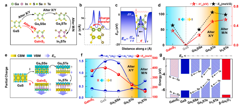
Fig. 1. The (a) schematic models, (b) planar-averaged charge density, (c) electrostatic potential, (d) ΔVin, Ein, (e) local wave function distributions, (f) carrier effective mass and Exb of Janus-MNXY monolayers. (d) The band levels of pristine isolated Janus-MNXY monolayers and β-Ga2O3 surface, respectively.
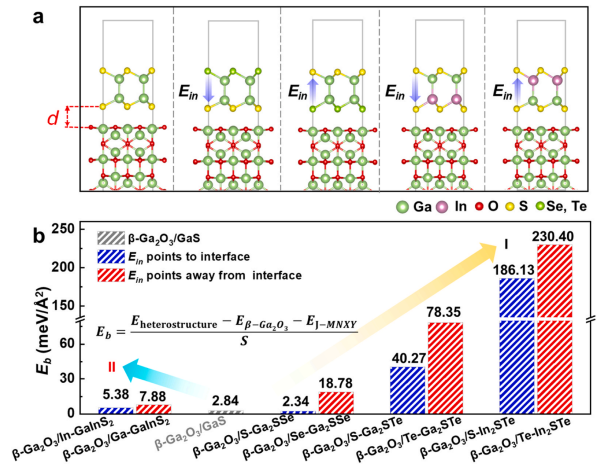
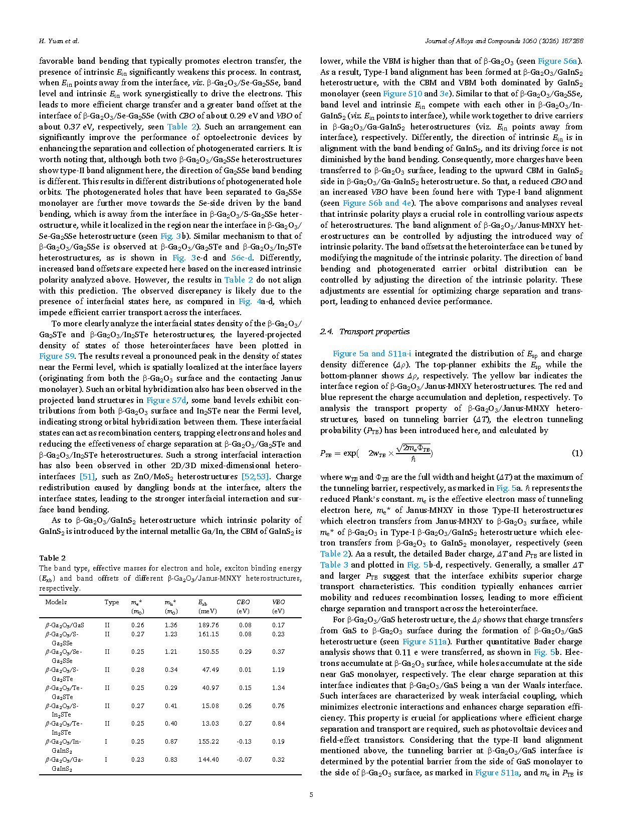
Fig. 2. (a) Structure models and (b) binding energies of β-Ga2O3/Janus-MNXY heterostructures, respectively.
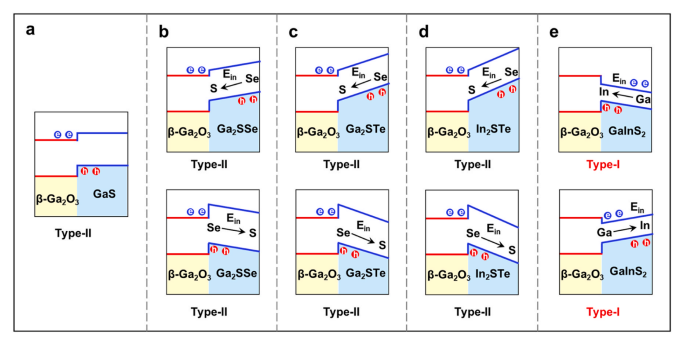
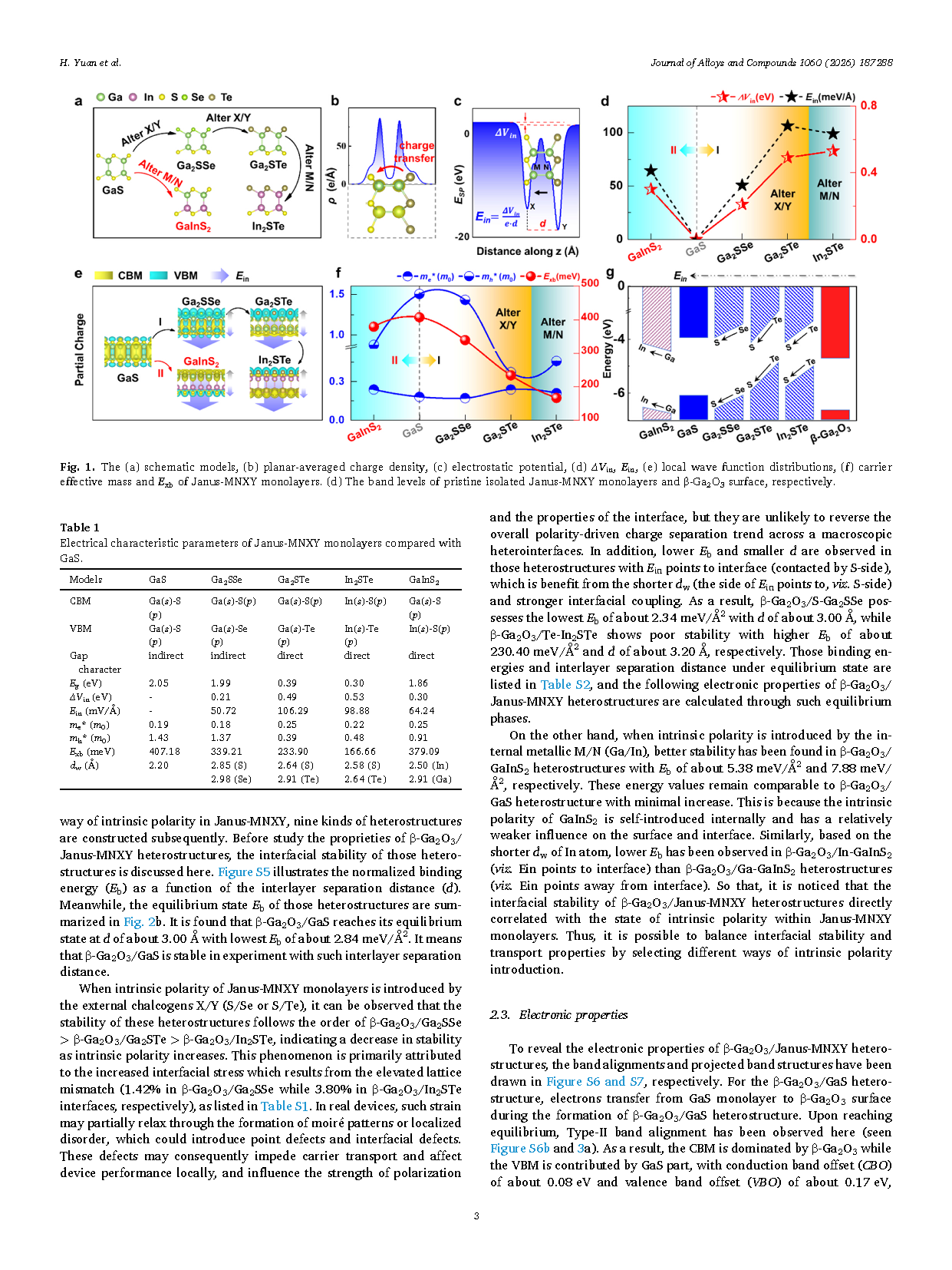
Fig. 3. The schematic band alignment for (a) β-Ga2O3/GaS, (b) β-Ga2O3/Ga2SSe, (c) β-Ga2O3/Ga2STe, (d) β-Ga2O3/In2STe and (e) β-Ga2O3/GaInS2 heterostructures, respectively. The top and bottom panels in (b-e) represent Ein points to interface and points away from interface, respectively.
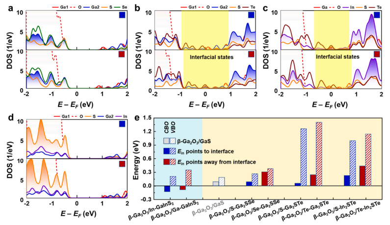
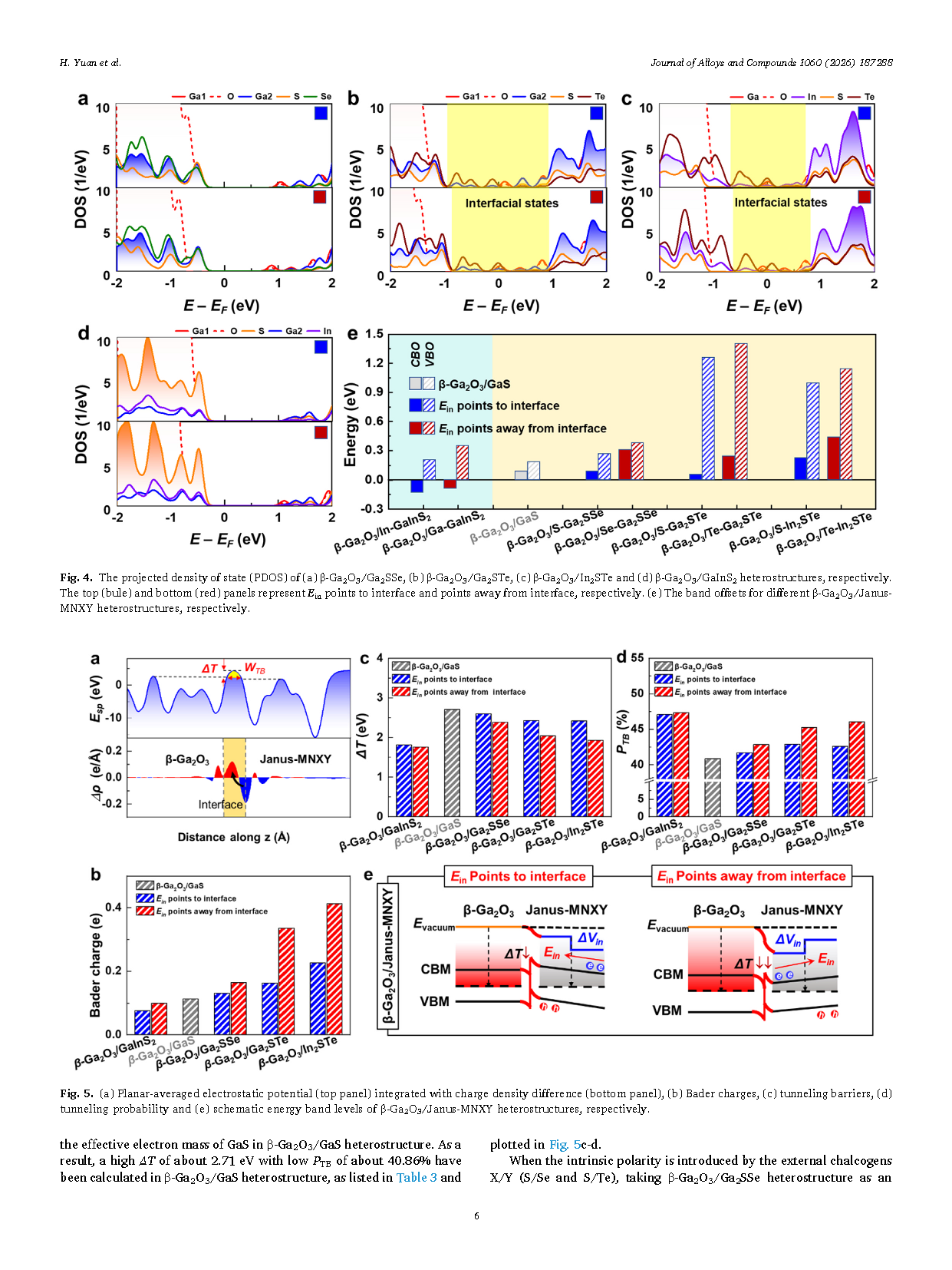
Fig. 4. The projected density of state (PDOS) of (a) β-Ga2O3/Ga2SSe, (b) β-Ga2O3/Ga2STe, (c) β-Ga2O3/In2O3STe and (d) β-Ga2O3/GaInS2 heterostructures, respectively. The top (bule) and bottom (red) panels represent Ein points to interface and points away from interface, respectively. (e) The band offsets for different β-Ga2O3/JanusMNXY heterostructures, respectively.
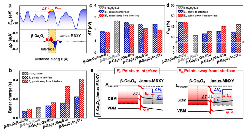
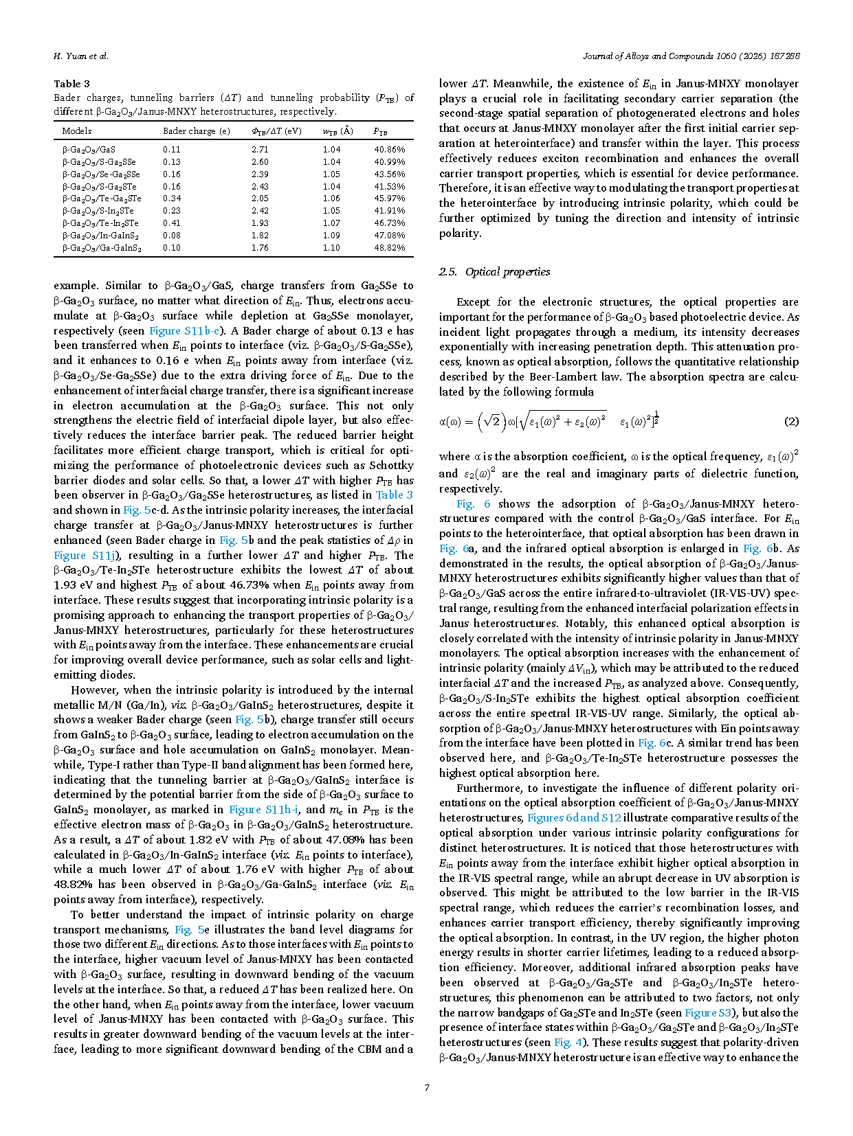
Fig. 5. (a) Planar-averaged electrostatic potential (top panel) integrated with charge density difference (bottom panel), (b) Bader charges, (c) tunneling barriers, (d) tunneling probability and (e) schematic energy band levels of β-Ga2O3/Janus-MNXY heterostructures, respectively.
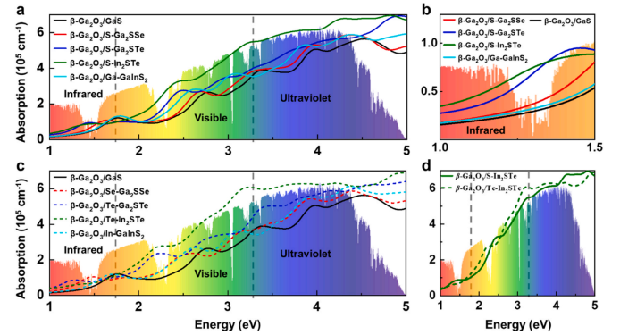
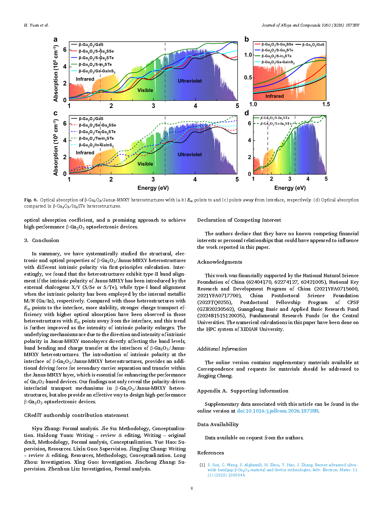
Fig. 6. Optical absorption of β-Ga2O3/Janus-MNXY heterostructures with (a-b) Ein points to and (c) points away from interface, respectively. (d) Optical absorption comparted in β-Ga2O3/In2STe heterostructures.
DOI:
doi.org/10.1016/j.jallcom.2026.187288