


Discover
【Knowledge Discover】The Evolution of Semiconductor Materials: From Silicon-Based Systems to Ultra-Wide Bandgap Semiconductors Represented by Gallium Oxide
日期:2026-03-20阅读:1001
Since the invention of the transistor, each generational evolution of semiconductor materials has profoundly reshaped human production and daily life. From the foundational role of first-generation silicon-based materials, to the optoelectronic breakthroughs driven by second-generation compound semiconductors, to the power electronics revolution enabled by third-generation wide bandgap materials, and now to the emerging fourth-generation ultra-wide bandgap semiconductors, every transition has been accompanied by the optimization of key physical parameters such as bandgap, breakdown electric field, and thermal conductivity. These advancements have collectively propelled leaps in computing, communications, energy systems, and applications in extreme environments.
This article reviews the evolution of semiconductor materials from the first to the fourth generation, analyzing the underlying physical logic and their industrial significance.
First-Generation Semiconductors: Silicon and Germanium — The Foundation of the Electronic Era
▲ (Germanium and single-crystal silicon)
Core materials: Germanium (Ge), single-crystal silicon (Si)
Key characteristics: Narrow bandgap (Si: 1.12 eV), mature processing technology, low cost, high stability
Industrial role: The foundational infrastructure of digital electronics
In 1947, Bell Labs fabricated the first transistor using a germanium crystal, marking the beginning of the electronic era. From the 1960s onward, silicon gradually replaced germanium as the dominant material due to its superior thermal stability, lower cost, and ease of purification.
First-generation materials laid the foundation for the invention of integrated circuits and the realization of Moore’s Law. From planar processing in the 1960s to today’s 3 nm technology nodes, silicon-based CMOS technology has increased transistor density to the trillion scale, with widespread applications in CPUs, memory, sensors, and consumer electronics, accounting for over 90% of the global semiconductor market. Silicon features a breakdown electric field of approximately 0.3 MV/cm and a thermal conductivity of about 1.5 W/cm·K, offering low cost and strong process compatibility.
However, its limitations are also evident. The narrow bandgap leads to a rapid increase in intrinsic carrier concentration at elevated temperatures, making it unsuitable for high-voltage, high-frequency, and high-temperature applications. In fields such as electric vehicles and 5G base stations, silicon-based devices tend to be bulky, exhibit higher power losses, and are approaching their physical limits.
Second-Generation Semiconductors: Gallium Arsenide and Indium Phosphide — Pioneers of Communications and Optoelectronics
▲ (Gallium arsenide)
 ▲ (Indium phosphide)
Core materials: Gallium arsenide (GaAs), indium phosphide (InP)
Key characteristics: High-frequency and high-speed performance, excellent optoelectronic properties, and electron mobility far exceeding that of silicon
Industrial breakthrough: Overcoming the high-frequency limitations of silicon and enabling wireless communications and optical interconnects

▲ (Military radar)
In response to the limitations of silicon in high-frequency and optoelectronic applications, second-generation compound semiconductors emerged. Gallium arsenide offers outstanding radio-frequency performance and is widely used in 5G/6G base stations, satellite communications, and radar systems. Indium phosphide, on the other hand, demonstrates superior performance in the 1310 nm and 1550 nm wavelength bands, supporting high-speed interconnects in global optical backbone networks and data centers.

▲ (Solar photovoltaics and energy storage)
Second-generation materials also laid the foundation for the optoelectronics industry. Early red LEDs, solar cells, and VCSEL-based LiDAR systems all relied on GaAs. Owing to their direct bandgap nature, these materials exhibit higher optoelectronic conversion efficiency than silicon, making them widely used in mobile communication base station power amplifiers (with efficiencies up to 65%), GPS systems, and fiber-optic networks.
Compared with first-generation semiconductors, second-generation materials represent a qualitative leap in high-frequency and optoelectronic performance. However, they also face notable limitations, including small wafer sizes (typically up to 6 inches), the presence of toxic elements, low thermal conductivity (GaAs: ~0.55 W/cm·K), and high cost, which restrict their large-scale application in power electronics.
Third-Generation Semiconductors: Silicon Carbide and Gallium Nitride — The Backbone of the Power Electronics Revolution
▲ (Silicon carbide material)
Core materials: Silicon carbide (SiC), gallium nitride (GaN)
Key characteristics: Wide bandgap (≥ 2.3 eV), high voltage and high temperature tolerance, low power loss, and high power density
Industrial role: The “enablers” of efficient energy conversion
Driven by the rapid growth of new energy, fast charging, and smart grids, third-generation semiconductors have emerged as conventional silicon devices approach their physical limits. With a combination of “three highs and two lows” — high voltage, high frequency, high temperature capability, and low loss, low resistance — these materials enable a fundamental performance leap:
Silicon carbide (SiC): Applied in high-voltage, high-power scenarios such as electric vehicle main drive inverters, photovoltaic inverters, and ultra-high-voltage (UHV) power grids
Gallium nitride (GaN): Targeted at high-frequency, high-efficiency applications such as fast chargers, 5G base station RF systems, and server power supplies
Applications are experiencing explosive growth. In electric vehicles, for example, Tesla Model 3 adopts SiC-based inverters, improving driving range by around 10%. In photovoltaics, fast-charging systems (with efficiency exceeding 92% and volume reduced by 50%), data center power supplies, radar, and satellite communications, third-generation materials are rapidly becoming mainstream. Meanwhile, GaN-enabled blue LEDs have triggered a revolution in solid-state lighting, significantly improving energy efficiency.
Third-generation semiconductors have expanded the role of semiconductors from “information processing” to “power conversion,” greatly enhancing energy utilization efficiency and providing critical support for carbon neutrality goals. As a result, the global SiC and GaN markets are growing rapidly, with China accelerating its industrial deployment.
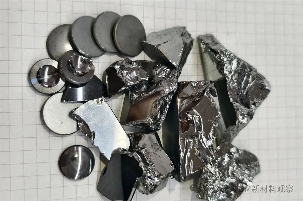
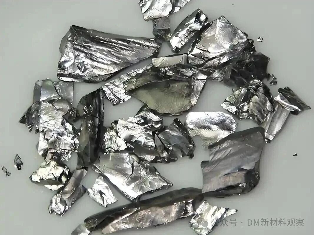
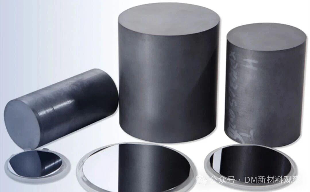
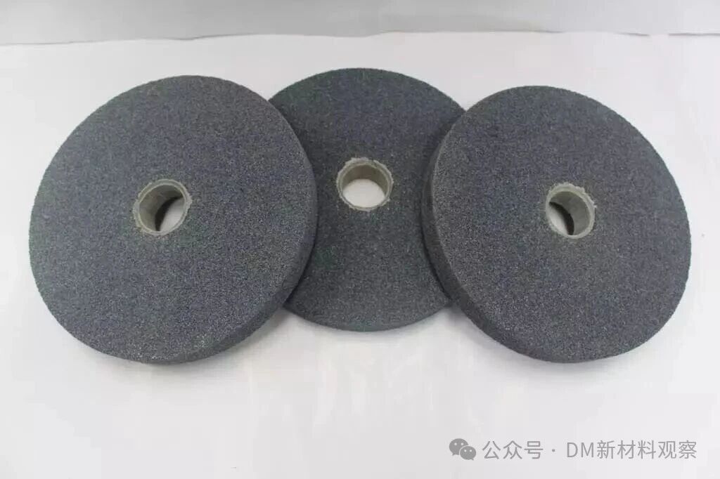
Fourth-Generation Semiconductors: The Ultra-Wide Bandgap Era Centered on Gallium Oxide
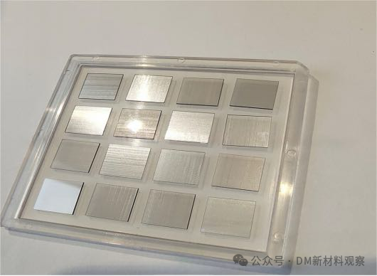
Core materials: Gallium oxide (Ga₂O₃), diamond, aluminum nitride (AlN)
Key features: Ultra-wide bandgap (>3.4 eV), extremely high breakdown field and thermal conductivity, targeting extreme operating conditions
Critical variable: Who can achieve large-scale commercialization first
Compared with the previous three generations, fourth-generation semiconductors are no longer just about incremental performance improvements—they are beginning to approach the physical limits of materials. Among them, gallium oxide is gradually emerging as the most practically viable material for industrial advancement.
From a materials physics perspective, gallium oxide exhibits a significantly higher breakdown electric field than SiC. Its theoretical Baliga figure of merit can reach approximately 10 times that of silicon carbide. This implies that, under the same voltage rating, devices can be made thinner with lower power loss, making it particularly suitable for ultra-high-voltage (multi-kV) power devices. This characteristic gives it the potential for a true “generation leap” in next-generation power electronics systems.
However, the real differentiator lies not only in performance, but in the manufacturing pathway. Unlike SiC and GaN, which rely on complex vapor-phase epitaxy, gallium oxide can be grown as large-size single crystals directly from the melt—a rare advantage among semiconductor materials. This melt-growth capability theoretically offers significant cost advantages and may enable lower costs than SiC once scaled.
At the device level, gallium oxide Schottky barrier diodes (SBDs) have already entered the engineering validation stage, while research on key structures such as MOSFETs is rapidly advancing. Its goal is not to replace all materials, but to establish an “irreplaceable domain” in the ultra-high-voltage regime (above the kV level).
In comparison:
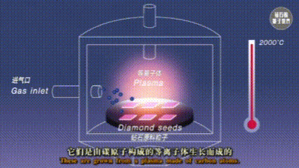
Diamond is closer to the “ultimate physical limit,” with thermal conductivity about 50 times that of silicon. However, due to challenges in doping and fabrication, it remains largely research-oriented in the near term.
Aluminum nitride (AlN) shows strong advantages in deep-ultraviolet optoelectronics and serves as a key material for specific niche applications.
As a result, differentiation is already emerging within fourth-generation semiconductors:
Ga₂O₃ → the most likely to achieve large-scale commercialization in power devices
Diamond → focused on extreme performance exploration
AlN → specialized optoelectronic applications
Looking further, technology routes around gallium oxide are also evolving. For example, heterogeneous integration structures such as Ga₂O₃-on-diamond aim to compensate for its thermal conductivity limitations. Once matured, such approaches could simultaneously address performance and heat dissipation bottlenecks, enabling true large-scale deployment.
In addition, fourth-generation materials are showing a parallel trend of “ultra-wide bandgap + ultra-narrow bandgap” development: on one end are extreme power materials represented by gallium oxide, and on the other are ultra-narrow bandgap materials such as antimonides, which play important roles in infrared detection, terahertz technologies, and quantum information.
Evolution Logic of Fourth-Generation Semiconductors
The increase in bandgap fundamentally represents enhanced electric field control capability
→ From silicon operating at the hundred-volt level to gallium oxide reaching the kilovolt range, this reflects a leap in humanity’s ability to control electrical energy
The application focus is shifting from “information” to “energy”
→ The third generation addresses “efficient power usage,” while the fourth generation begins to tackle “extreme power conditions”
The real dividing line for the fourth generation lies not in performance, but in the path to industrialization
→ Whoever achieves large-size, low-cost production will take the lead
→ At present, gallium oxide appears to be the most likely to break through first
Conclusion
From the widespread adoption of silicon, to the efficiency improvements enabled by wide bandgap materials, and now to ultra-wide bandgap materials approaching physical limits, the evolution of semiconductor materials essentially reflects humanity’s continuous advancement in controlling energy and information.
Today, third-generation semiconductors are entering a phase of large-scale expansion, while among fourth-generation materials, gallium oxide has already moved beyond the laboratory and is approaching early-stage industrialization.
This suggests that the next wave of transformation in semiconductors may not be merely a performance upgrade, but a structural reconfiguration of the entire power electronics paradigm.
